This document discusses passive devices used in RFIC design, including inductors, capacitors, and resistors. It covers topics like:
- Different types of inductors and their modeling approaches. Enhancing inductor Q factors by reducing metal and substrate losses.
- Varactors/tunable capacitors using junctions and accumulation modes. Their Q factors and tuning ranges as a function of bias.
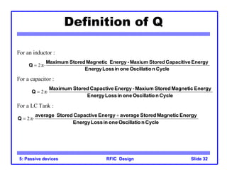
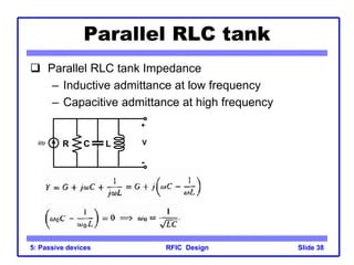
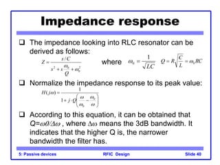
- RC and RLC networks, including their impedance transformations between series and parallel configurations. Definitions of Q factor for different passive components and networks.


![RF Module Design - [Chapter 7] Voltage-Controlled Oscillator](https://cdn.slidesharecdn.com/ss_thumbnails/rfch7-150613070347-lva1-app6892-thumbnail.jpg?width=640&height=640&fit=bounds)


![RF Module Design - [Chapter 5] Low Noise Amplifier](https://cdn.slidesharecdn.com/ss_thumbnails/rfch5-150613070346-lva1-app6891-thumbnail.jpg?width=640&height=640&fit=bounds)


![RF Circuit Design - [Ch2-1] Resonator and Impedance Matching](https://cdn.slidesharecdn.com/ss_thumbnails/ch2-1-150613064353-lva1-app6892-thumbnail.jpg?width=640&height=640&fit=bounds)