Download as PDF, PPTX
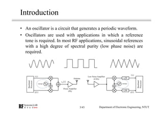
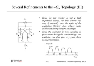
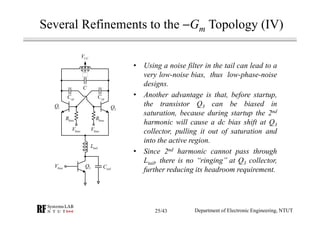
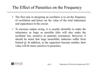
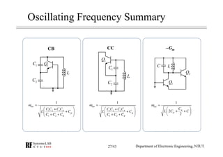

This document discusses the design of voltage-controlled oscillators in RF transceiver modules, focusing on critical components such as resonators, feedback loops, and amplifier configurations. It emphasizes the importance of sustaining oscillations through negative resistance and feedback mechanisms to achieve high spectral purity. Various oscillator topologies, capacitor ratios, and conditions for oscillation are also detailed, along with practical considerations for implementation and performance evaluation.
![RF Module Design - [Chapter 1] From Basics to RF Transceivers](https://cdn.slidesharecdn.com/ss_thumbnails/rfch1-150613070344-lva1-app6892-thumbnail.jpg?width=640&height=640&fit=bounds)
![RF Module Design - [Chapter 3] Linearity](https://cdn.slidesharecdn.com/ss_thumbnails/rfch3-150613070345-lva1-app6891-thumbnail.jpg?width=640&height=640&fit=bounds)
![RF Circuit Design - [Ch4-2] LNA, PA, and Broadband Amplifier](https://cdn.slidesharecdn.com/ss_thumbnails/ch4-2-150613064410-lva1-app6891-thumbnail.jpg?width=640&height=640&fit=bounds)
![RF Module Design - [Chapter 2] Noises](https://cdn.slidesharecdn.com/ss_thumbnails/rfch2-150613070344-lva1-app6892-thumbnail.jpg?width=640&height=640&fit=bounds)
![RF Circuit Design - [Ch3-2] Power Waves and Power-Gain Expressions](https://cdn.slidesharecdn.com/ss_thumbnails/ch3-2-150613064404-lva1-app6891-thumbnail.jpg?width=640&height=640&fit=bounds)
![Multiband Transceivers - [Chapter 3] Basic Concept of Comm. Systems](https://cdn.slidesharecdn.com/ss_thumbnails/ch3-150613070933-lva1-app6892-thumbnail.jpg?width=640&height=640&fit=bounds)
![Circuit Network Analysis - [Chapter1] Basic Circuit Laws](https://cdn.slidesharecdn.com/ss_thumbnails/ch1-150613063856-lva1-app6892-thumbnail.jpg?width=640&height=640&fit=bounds)
![RF Module Design - [Chapter 5] Low Noise Amplifier](https://cdn.slidesharecdn.com/ss_thumbnails/rfch5-150613070346-lva1-app6891-thumbnail.jpg?width=640&height=640&fit=bounds)
![RF Module Design - [Chapter 8] Phase-Locked Loops](https://cdn.slidesharecdn.com/ss_thumbnails/rfch8-150613070348-lva1-app6892-thumbnail.jpg?width=640&height=640&fit=bounds)


![射頻電子 - [第三章] 史密斯圖與阻抗匹配](https://cdn.slidesharecdn.com/ss_thumbnails/ch3-150613065103-lva1-app6892-thumbnail.jpg?width=640&height=640&fit=bounds)
![RF Circuit Design - [Ch1-2] Transmission Line Theory](https://cdn.slidesharecdn.com/ss_thumbnails/ch1-2-150613064349-lva1-app6892-thumbnail.jpg?width=640&height=640&fit=bounds)

![Multiband Transceivers - [Chapter 2] Noises and Linearities](https://cdn.slidesharecdn.com/ss_thumbnails/ch2-150613070933-lva1-app6892-thumbnail.jpg?width=640&height=640&fit=bounds)
![RF Circuit Design - [Ch2-1] Resonator and Impedance Matching](https://cdn.slidesharecdn.com/ss_thumbnails/ch2-1-150613064353-lva1-app6892-thumbnail.jpg?width=640&height=640&fit=bounds)
![RF Circuit Design - [Ch4-1] Microwave Transistor Amplifier](https://cdn.slidesharecdn.com/ss_thumbnails/ch4-1-150613064409-lva1-app6892-thumbnail.jpg?width=640&height=640&fit=bounds)

![Multiband Transceivers - [Chapter 7] Multi-mode/Multi-band GSM/GPRS/TDMA/AMP...](https://cdn.slidesharecdn.com/ss_thumbnails/ch7-150613070936-lva1-app6892-thumbnail.jpg?width=640&height=640&fit=bounds)
![射頻電子 - [實驗第一章] 基頻放大器設計](https://cdn.slidesharecdn.com/ss_thumbnails/e1-150613065108-lva1-app6892-thumbnail.jpg?width=640&height=640&fit=bounds)
![射頻電子 - [第一章] 知識回顧與通訊系統簡介](https://cdn.slidesharecdn.com/ss_thumbnails/ch1-150613065058-lva1-app6891-thumbnail.jpg?width=640&height=640&fit=bounds)
![Multiband Transceivers - [Chapter 1]](https://cdn.slidesharecdn.com/ss_thumbnails/ch1-150613070932-lva1-app6891-thumbnail.jpg?width=640&height=640&fit=bounds)


![Agilent ADS 模擬手冊 [實習3] 壓控振盪器模擬](https://cdn.slidesharecdn.com/ss_thumbnails/3adsosc-150613072819-lva1-app6892-thumbnail.jpg?width=640&height=640&fit=bounds)

![RF Circuit Design - [Ch3-1] Microwave Network](https://cdn.slidesharecdn.com/ss_thumbnails/ch3-1-150613064402-lva1-app6892-thumbnail.jpg?width=640&height=640&fit=bounds)
![RF Module Design - [Chapter 6] Power Amplifier](https://cdn.slidesharecdn.com/ss_thumbnails/rfch6-150613070347-lva1-app6891-thumbnail.jpg?width=640&height=640&fit=bounds)
![[ZigBee 嵌入式系統] ZigBee 應用實作 - 使用 TI Z-Stack Firmware](https://cdn.slidesharecdn.com/ss_thumbnails/zigbeeappimplementation-150613072040-lva1-app6891-thumbnail.jpg?width=640&height=640&fit=bounds)
![[嵌入式系統] MCS-51 實驗 - 使用 IAR (2)](https://cdn.slidesharecdn.com/ss_thumbnails/mcs51iarpart2-150613071717-lva1-app6891-thumbnail.jpg?width=640&height=640&fit=bounds)
![Multiband Transceivers - [Chapter 5] Software-Defined Radios](https://cdn.slidesharecdn.com/ss_thumbnails/ch5-150613070934-lva1-app6892-thumbnail.jpg?width=640&height=640&fit=bounds)
![[嵌入式系統] MCS-51 實驗 - 使用 IAR (3)](https://cdn.slidesharecdn.com/ss_thumbnails/mcs51iarpart3-150613071723-lva1-app6892-thumbnail.jpg?width=640&height=640&fit=bounds)

![[嵌入式系統] MCS-51 實驗 - 使用 IAR (1)](https://cdn.slidesharecdn.com/ss_thumbnails/mcs51iarpart1-150613071712-lva1-app6892-thumbnail.jpg?width=640&height=640&fit=bounds)

![RF Module Design - [Chapter 4] Transceiver Architecture](https://cdn.slidesharecdn.com/ss_thumbnails/rfch4-150613070346-lva1-app6891-thumbnail.jpg?width=640&height=640&fit=bounds)
![[嵌入式系統] 嵌入式系統進階](https://cdn.slidesharecdn.com/ss_thumbnails/advembedded-150613071653-lva1-app6892-thumbnail.jpg?width=640&height=640&fit=bounds)
![[ZigBee 嵌入式系統] ZigBee Architecture 與 TI Z-Stack Firmware](https://cdn.slidesharecdn.com/ss_thumbnails/zigbeearchitecture-150613072045-lva1-app6892-thumbnail.jpg?width=640&height=640&fit=bounds)
![Multiband Transceivers - [Chapter 7] Spec. Table](https://cdn.slidesharecdn.com/ss_thumbnails/ch7table-150613070936-lva1-app6892-thumbnail.jpg?width=640&height=640&fit=bounds)
![Multiband Transceivers - [Chapter 6] Multi-mode and Multi-band Transceivers](https://cdn.slidesharecdn.com/ss_thumbnails/ch6-150613070935-lva1-app6891-thumbnail.jpg?width=640&height=640&fit=bounds)
![Multiband Transceivers - [Chapter 4] Design Parameters of Wireless Radios](https://cdn.slidesharecdn.com/ss_thumbnails/ch4-150613070934-lva1-app6892-thumbnail.jpg?width=640&height=640&fit=bounds)
![射頻電子 - [實驗第三章] 濾波器設計](https://cdn.slidesharecdn.com/ss_thumbnails/e3-150613065109-lva1-app6891-thumbnail.jpg?width=640&height=640&fit=bounds)
![射頻電子 - [實驗第四章] 微波濾波器與射頻多工器設計](https://cdn.slidesharecdn.com/ss_thumbnails/e4-150613065110-lva1-app6892-thumbnail.jpg?width=640&height=640&fit=bounds)
![射頻電子 - [實驗第二章] I/O電路設計](https://cdn.slidesharecdn.com/ss_thumbnails/e2-150613065108-lva1-app6892-thumbnail.jpg?width=640&height=640&fit=bounds)


![Agilent ADS 模擬手冊 [實習2] 放大器設計](https://cdn.slidesharecdn.com/ss_thumbnails/2adsamp-150613072818-lva1-app6892-thumbnail.jpg?width=640&height=640&fit=bounds)
![Agilent ADS 模擬手冊 [實習1] 基本操作與射頻放大器設計](https://cdn.slidesharecdn.com/ss_thumbnails/1adsbasics-150613072812-lva1-app6891-thumbnail.jpg?width=640&height=640&fit=bounds)
![射頻電子實驗手冊 - [實驗8] 低雜訊放大器模擬](https://cdn.slidesharecdn.com/ss_thumbnails/simlab8-150613072425-lva1-app6891-thumbnail.jpg?width=640&height=640&fit=bounds)
![射頻電子實驗手冊 - [實驗7] 射頻放大器模擬](https://cdn.slidesharecdn.com/ss_thumbnails/simlab7-150613072420-lva1-app6892-thumbnail.jpg?width=640&height=640&fit=bounds)
![射頻電子實驗手冊 [實驗6] 阻抗匹配模擬](https://cdn.slidesharecdn.com/ss_thumbnails/simlab6-150613072411-lva1-app6892-thumbnail.jpg?width=640&height=640&fit=bounds)
![射頻電子實驗手冊 [實驗1 ~ 5] ADS入門, 傳輸線模擬, 直流模擬, 暫態模擬, 交流模擬](https://cdn.slidesharecdn.com/ss_thumbnails/simlab15-150613072411-lva1-app6892-thumbnail.jpg?width=640&height=640&fit=bounds)


