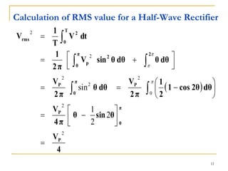
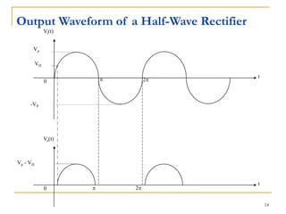
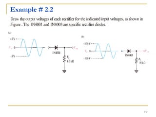
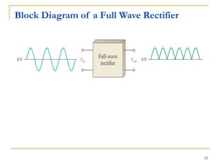
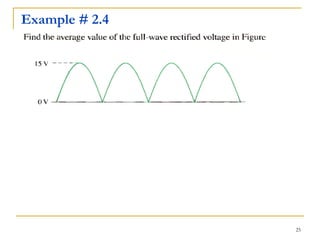
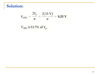
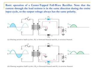
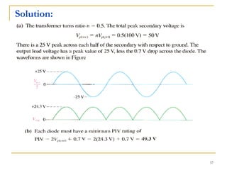
1
DIODE APPLICATIONS
Thursday, November 10, 2022
CHAPTER NO. 02
By: Engr. Salman Hameed Yousafzai
2
BASIC DC POWER SUPPLY
3
Block diagram of a basic DC power supply with a load.
4
HALF-WAVE RECTIFIER (HWR)
5
Block diagram of a Half Wave Rectifier
6
Half-Wave Rectifier operation. The diode is considered to be ideal
7
Average value of the Half-Wave Rectified signal.
8
Calculation of Average value for a Half-Wave Rectifier
 
π
V
θ
cos
2π
V
dθ
0
dθ
θ
sin
V
2π
1
dt
V
T
1
V
P
π
0
P
2
π
0
p
T
0
DC
=
−
=





 +
=
=





9
Example # 2.1
10
Solution:
11
( )
4
V
θ
sin
θ
π
4
V
dθ
2θ
cos
1
2
1
π
2
V
dθ
θ
π
2
V
dθ
0
dθ
θ
sin
V
π
2
1
dt
V
T
1
V
P
π
0
P
P
π
0
P
2
π
0
2
p
T
0
2
rms
2
2
0
2
2
2
2
2
2
2
1
sin
=






−
=






−
=
=





 +
=
=








Calculation of RMS value for a Half-Wave Rectifier
12
VDC
Vrms
t0
t1
t2
t3
Vp
VO
t
DC & RMS Level on Waveform of a HWR
13
The effect of the barrier potential on the half-wave rectified
output voltage is to reduce the peak value of the input by
about 0.7 V.
14
Vp
0
-VP
 2
Vi(t)
t
VD
Vp - VD
0  2
Vo(t)
t
Output Waveform of a Half-Wave Rectifier
15
Example # 2.2
16
Solution:
17
The PIV occurs at the peak of each half-cycle of the input
voltage when the diode is reverse-biased. In this circuit, the
PIV occurs at the peak of each negative half-cycle.
18
Half-Wave Rectifier with transformer-coupled input voltage.
19
Example # 2.3
20
Solution:
21
FULL-WAVE RECTIFIER (FWR)
22
Block Diagram of a Full Wave Rectifier
23
Vp
0
-VP
 2
Vi(t)
t
Vp - VD
0  2
Vo(t)
t
23
Dr. RS Thursday, November 10, 2022
Output Waveform of a Full Wave Rectifier
24
Calculation of Average value for a Full-Wave Rectifier
 
π
V
2
θ
cos
π
V
dθ
θ
sin
V
π
1
dt
V
T
1
V
P
π
0
P
π
0
p
T
0
DC
=
−
=
=
=


25
Example # 2.4
26
Solution:
27
Calculation of RMS value for a Full -Wave Rectifier
( )
2
V
θ
sin
θ
π
2
V
dθ
2θ
cos
1
2
1
π
V
dθ
θ
sin
V
π
1
dt
V
T
1
V
P
π
0
P
P
π
0
2
p
T
0
2
rms
2
2
0
2
2
2
2
2
1
=






−
=






−
=
=
=




28
Types of Full-Wave Rectifier
◼ Center-Tapped Full Wave Rectifier
◼ Bridge Full Wave Rectifier
29
CENTER-TAPPED FULL-WAVE RECTIFIER
30
Circuit Diagram of a Center-Tapped Full-Wave Rectifier
31
Basic operation of a Center-Tapped Full-Wave Rectifier. Note that the
current through the load resistor is in the same direction during the entire
input cycle, so the output voltage always has the same polarity.
32
Center-tapped full-wave rectifier with a transformer turns ratio of 1.
Vp(pri) is the peak value of the primary voltage.
33
Center-tapped full-wave rectifier with a transformer turns ratio
of 2.
34
PIV of a Center Tapped Full Wave Rectifier
35
Calculation of PIV for a Center Tapped Full Wave Rectifier
36
Example # 2.5
37
Solution:
38
BRIDGE FULL -WAVE RECTIFIER
39
Circuit Diagram of a Bridge Full-Wave Rectifier
40
Basic Operation of a Bridge Full Wave Rectifier
Thursday, November 10, 2022
41
Bridge Output Voltage with Ideal & Practical Diodes
Thursday, November 10, 2022
42
Peak inverse voltages across diodes D3 and D4 in a bridge
rectifier during the positive half-cycle of the secondary voltage.
Thursday, November 10, 2022
43
Formulas For Bridge Full Wave Rectifier
1. Vpout = Vp (sec) { for ideal case }
2. Vpout =Vp (sec) – 1.4v { for practical case }
3. PIV = Vpout { for ideal case }
4. PIV = Vpout + 0.7v { for practical case }
44
Example # 2.6
45
Solution:
46
POWER SUPPLY FILTERS
47
Basic Principle of Power Supply Filter
◼ A power supply filter ideally eliminates the fluctuations in the output
voltage of a half wave or full wave rectifier and produces a constant level
dc voltage
◼ Filtering is necessary because electronic circuits require a constant
source of dc voltage and current to provide power and biasing for proper
operation
Ripple is a Small amount
of Fluctuations in the filter
48
Capacitor Input Filter/ Pi(π) Filter
◼ A Half Wave rectifier with a capacitor–input filter is shown in figure
◼ The filter is simply a capacitor connected from the rectifier output
to ground.
◼ RL represents the equivalent resistance of a load
Dr. RS
49
Operation of a half-wave rectifier with a capacitor-input filter. The current
indicates charging or discharging of the capacitor.
Thursday, November 10, 2022
50
Ripple Voltage (Vr)
◼ Variation in the capacitor voltage due to the charging and
discharging is called the ripple voltage
◼ Generally, ripple is undesirable, so the smaller the ripple, the
better the filtering action
Dr. RS
Half-wave ripple voltage (green line).
51
Comparison of ripple voltages for half-wave and full-wave
rectified voltages with the same filter capacitor and load and
derived from the same sinusoidal input voltage.
Thursday, November 10, 2022
52
The frequency of a full-wave rectified voltage is twice that of a
half-wave rectified voltage.
Thursday, November 10, 2022
53
Ripple Factor (r)
◼ Indication of the effectiveness of the filter is called the ripple factor
Dr. RS
Note: The lower the ripple factor , the better the filter.
Where Vr(pp) : peak to peak ripple voltage
VDC : average value of ripple voltage
How
54
Effects of C and RL on Ripple factor
Thursday, November 10, 2022
C=1000µF C=470µF
C=100µF
R=1500Ω
R=1000Ω
R=500Ω
b) Effect on RL
a) Effect on C
The ripple factor can be lowered by increasing the value of
the filter capacitor or increasing the load resistance
55
Formulas of Ripple factor for HWR & FWR

rhwr =
Vr( pp)
VDC
=
1
2 3 fRLC
Dr. RS Thursday, November 10, 2022

rfwr =
Vr(pp)
VDC
=
1
4 3 fRLC
56
Formulas of Vr(pp) and VDC for a Full Wave Rectifier
with Capacitor Input Filter
Vp(rect) : unfiltered peak rectified voltage
Vr(pp) : peak to peak ripple voltage
VDC : average value of ripple voltage
Thursday, November 10, 2022

Chapter 02.pdf