This document discusses high efficiency power amplifier technologies. It describes:
1) The requirements for future power amplifiers including high linearity, output power, bandwidth, and reduced energy consumption.
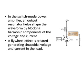
2) How switch-mode power amplifier technology using pulse width modulation can achieve up to 90% efficiency but is limited to low frequencies.
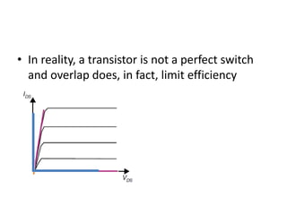
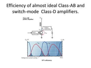
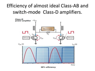
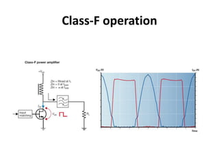
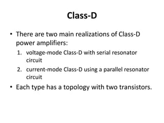
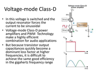
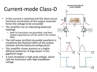
3) Different classes of switch-mode power amplifier operation (Class D, E, and F) and how they work to achieve high efficiency by minimizing voltage-current overlap losses.
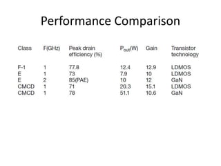
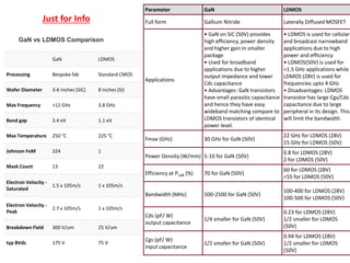
4) Performance comparisons of different technologies like GaN and LDMOS transistors, noting advantages like bandwidth and efficiency of GaN for radio applications.


![RF Module Design - [Chapter 4] Transceiver Architecture](https://cdn.slidesharecdn.com/ss_thumbnails/rfch4-150613070346-lva1-app6891-thumbnail.jpg?width=640&height=640&fit=bounds)
![RF Module Design - [Chapter 6] Power Amplifier](https://cdn.slidesharecdn.com/ss_thumbnails/rfch6-150613070347-lva1-app6891-thumbnail.jpg?width=640&height=640&fit=bounds)


![RF Circuit Design - [Ch4-2] LNA, PA, and Broadband Amplifier](https://cdn.slidesharecdn.com/ss_thumbnails/ch4-2-150613064410-lva1-app6891-thumbnail.jpg?width=640&height=640&fit=bounds)

![RF Module Design - [Chapter 1] From Basics to RF Transceivers](https://cdn.slidesharecdn.com/ss_thumbnails/rfch1-150613070344-lva1-app6892-thumbnail.jpg?width=640&height=640&fit=bounds)

![RF Module Design - [Chapter 3] Linearity](https://cdn.slidesharecdn.com/ss_thumbnails/rfch3-150613070345-lva1-app6891-thumbnail.jpg?width=640&height=640&fit=bounds)


![RF Module Design - [Chapter 5] Low Noise Amplifier](https://cdn.slidesharecdn.com/ss_thumbnails/rfch5-150613070346-lva1-app6891-thumbnail.jpg?width=640&height=640&fit=bounds)


![[Deck] What's New in Spark-Iceberg Integration via DSV2.pptx](https://cdn.slidesharecdn.com/ss_thumbnails/deckwhatsnewinspark-icebergintegrationviadsv2-260210005337-25955b12-thumbnail.jpg?width=640&height=640&fit=bounds)


