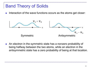
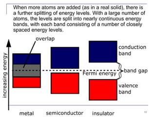
SlideShare a Scribd company logo
1
 11.1 Band Theory of Solids
 11.2 Semiconductor Theory
 11.3 Semiconductor Devices
 11.4 Nanotechnology
CHAPTER 11
Semiconductor Theory and Devices
It is evident that many years of research by a great many people, both
before and after the discovery of the transistor effect, has been required
to bring our knowledge of semiconductors to its present development.
We were fortunate to be involved at a particularly opportune time and to
add another small step in the control of Nature for the benefit of mankind.
- John Bardeen, 1956 Nobel lecture
2
11.1: Band Theory of Solids
 In Chapter 10 you learned about structural, thermal,
and magnetic properties of solids.
In this chapter we concentrate on electrical
conduction.
3
Categories of Solids
 There are three categories of solids, based on their
conducting properties:
 conductors
 semiconductors
 insulators
4
Electrical Resistivity
and Conductivity of
Selected Materials
at 293 K
5
Reviewing the previous table reveals that:
 The electrical conductivity at room temperature is
quite different for each of these three kinds of solids
 Metals and alloys have the highest conductivities
 followed by semiconductors
 and then by insulators
6
Semiconductor Conduction
 The free-electron model from Chapter 9 does not
apply to semiconductors and insulators, since these
materials simply lack free electrons to conduct in a
free-electron mode, this is due to the nature of the
bond in the crystals
There is a different conduction mechanism for
semiconductors than for normal conductors.
7
Resistivity vs. Temperature
Figure 11.1: (a) Resistivity versus temperature for a typical conductor. Notice the linear rise in
resistivity with increasing temperature at all but very low temperatures. (b) Resistivity versus
temperature for a typical conductor at very low temperatures. Notice that the curve flattens and
approaches a nonzero resistance as T → 0. (c) Resistivity versus temperature for a typical
semiconductor. The resistivity increases dramatically as T → 0.
8
 In order to account for decreasing resistivity with
increasing temperature as well as other properties of
semiconductors, a new theory known as the band
theory is introduced.
 The essential feature of the band theory is that the
allowed energy states for electrons are nearly
continuous over certain ranges, called energy bands,
with forbidden energy gaps between the bands.
Band Theory of Solids
9
 Consider initially the known wave functions of two
hydrogen atoms far enough apart so that they do
not interact.
Band Theory of Solids
10
Band Theory of Solids
 Interaction of the wave functions occurs as the atoms get closer:
 An electron in the symmetric state has a nonzero probability of
being halfway between the two atoms, while an electron in the
antisymmetric state has a zero probability of being at that location.
Symmetric Antisymmetric
11
Band Theory of Solids
 In the symmetric case the binding energy is
slightly stronger resulting in a lower energy
state.
 Thus there is a splitting of all possible energy
levels (1s, 2s, and so on).
12
When more atoms are added (as in a real solid), there is
a further splitting of energy levels. With a large number of
atoms, the levels are split into nearly continuous energy
bands, with each band consisting of a number of closely
spaced energy levels.
13
Kronig-Penney Model
 An effective way to understand the energy gap in
semiconductors is to model the interaction between
the electrons and the structure of the crystal where
atoms or groups of atoms are arranged on nodes of
a 3D periodic lattice and vibrate around their
equilibrium positions
 R. de L. Kronig and W. G. Penney developed a
useful one-dimensional model of the electron lattice
interaction in 1931.
14
Kronig-Penney Model
 Kronig and Penney assumed that an electron
experiences an infinite one-dimensional array of finite
potential wells.
 Each potential well models attraction to an atom in the
periodic structure, so the size of the wells must
correspond roughly to the lattice spacing in element
semiconductors.
15
Kronig-Penney Model
 Since the electrons are not free their energies are less
than the height V0 of each of the potentials, but the
electron is essentially free in the region 0 < x < a,
where it has a wave function of the form
where the wave number k is given by the usual
relation:
16
Tunneling
 In the region between a < x < a + b the electron can
tunnel through and the wave function loses its
oscillatory solution and becomes that of an
evanescent wave
17
Kronig-Penney Model
 Matching solutions at the boundary, Kronig and
Penney find
Here K is another wave number.
18
 The left-hand side is limited to values between +1 and
−1 for all values of K.
 Plotting this it is observed there exist restricted (shaded)
forbidden zones for solutions.
Kronig-Penney Model
19
Figure 11.5 (a) Plot of the left side of
Equation (11.3) versus ka for κ2ba / 2 =
3π / 2. Allowed energy values must
correspond to the values of k for
for which the plotted
function lies between -1 and +1.
Forbidden values are shaded in light
blue. (b) The corresponding plot of
energy versus ka for κ2ba / 2 = 3π / 2,
showing the forbidden energy zones
(gaps).
The Forbidden Zones
20
Important differences between the Kronig-
Penney model and the single potential well
1) For an infinite crystal structure (translation periodic lattice)
the allowed energies within each band are continuous
rather than discrete. In a real crystal the lattice is not
infinite, but even if chains are thousands of atoms long,
the allowed energies are nearly continuous.
2) In a real three-dimensional crystal it is appropriate to
speak of a wave vector . The allowed ranges for
constitute what are referred to in solid state theory as
Brillouin zones.
k
k
21
And…
3) In a real crystal the potential function is more
complicated than the Kronig-Penney squares. Thus, the
energy gaps are by no means uniform in size. The gap
sizes can be changed by the introduction of impurities
or imperfections of the lattice.
 These facts concerning the energy gaps are of
paramount importance in understanding the electronic
behavior of semiconductors.
22
Band Theory and Conductivity
 Band theory helps us understand what makes a
conductor, insulator, or semiconductor.
1) Good conductors like copper can be understood using the free
electron
2) It is also possible to make a conductor using a material with its
highest band filled, in which case no electron in that band can be
considered free.
3) If this filled band overlaps with the next higher band, however (so that
effectively there is no gap between these two bands) then an applied
electric field can make an electron from the filled band jump to the
higher level.
 This allows conduction to take place, although typically
with slightly higher resistance than in normal metals. Such
materials are known as semimetals.
23
Valence and Conduction Bands
 The band structures of insulators and semiconductors
resemble each other qualitatively. Normally there exists in
both insulators and semiconductors a filled energy band
(referred to as the valence band) separated from the next
higher band (referred to as the conduction band) by an
energy gap.
 If this gap is at least several electron volts, the material is
an insulator. It is too difficult for an applied field to
overcome that large an energy gap, and thermal excitations
lack the energy to promote sufficient numbers of electrons
to the conduction band.
24
 For energy gaps smaller than about 1 electron volt,
it is possible for enough electrons to be excited
thermally into the conduction band, so that an
applied electric field can produce a modest current.
The result is a semiconductor.
Smaller energy gaps create semiconductors
25
11.2: Semiconductor Theory
 At T = 0 we expect all of the atoms in a solid to be in the
ground state. The distribution of electrons (fermions) at
the various energy levels is governed by the Fermi-Dirac
distribution of Equation (9.34):
β = (kT)−1 and EF is the Fermi energy.
26
Temperature and Resistivity
 When the temperature is increased from T = 0, more and more
atoms are found in excited states.
 The increased number of electrons in excited states explains the
temperature dependence of the resistivity of semiconductors.
Only those electrons that have jumped from the valence band to
the conduction band are available to participate in the
conduction process in a semiconductor. More and more
electrons are found in the conduction band as the temperature is
increased, and the resistivity of the semiconductor therefore
decreases.
27
Some Observations
 Although it is not possible to use the Fermi-Dirac factor to derive an exact
expression for the resistivity of a semiconductor as a function of
temperature, some observations follow:
1) The energy E in the exponential factor makes it clear why the band gap is
so crucial. An increase in the band gap by a factor of 10 (say from 1 eV to
10 eV) will, for a given temperature, increase the value of exp(βE) by a
factor of exp(9βE).
 This generally makes the factor FFD so small
that the material has to be an insulator.
2) Based on this analysis, the resistance of a semiconductor is expected to
decrease exponentially with increasing temperature.
 This is approximately true—although not exactly, because the function
FFD is not a simple exponential, and because the band gap does vary
somewhat with temperature.
28
Clement-Quinnell Equation
 A useful empirical expression developed by Clement
and Quinnell for the temperature variation of standard
carbon resistors is given by
where A, B, and K are constants.
29
Test of the Clement-Quinnell Equation
Figure 11.7: (a) An experimental test of the Clement-Quinnell equation, using resistance versus
temperature data for four standard carbon resistors. The fit is quite good up to 1 / T ≈ 0.6,
corresponding to T ≈ 1.6 K. (b) Resistance versus temperature curves for some thermometers used in
research. A-B is an Allen-Bradley carbon resistor of the type used to produce the curves in (a). Speer
is a carbon resistor, and CG is a carbon-glass resistor. Ge 100 and 1000 are germanium resistors.
From G. White, Experimental Techniques in Low Temperature Physics, Oxford: Oxford University
Press (1979).
30
Holes and Intrinsic Semiconductors
 When electrons move into the conduction band, they leave behind
vacancies in the valence band. These vacancies are called holes.
Because holes represent the absence of negative charges, it is useful
to think of them as positive charges.
 Whereas the electrons move in a direction opposite to the applied
electric field, the holes move in the direction of the electric field.
 A semiconductor in which there is a balance between the number of
electrons in the conduction band and the number of holes in the
valence band is called an intrinsic semiconductor.
Examples of intrinsic semiconductors include pure carbon and
germanium.
31
Impurity Semiconductor
 It is possible to fine-tune a semiconductor’s properties by adding a small
amount of another material, called a dopant, to the semiconductor
creating what is a called an impurity semiconductor.
 As an example, silicon has four electrons in its outermost shell (this
corresponds to the valence band) and arsenic has five.
Thus while four of arsenic’s outer-shell electrons participate in covalent
bonding with its nearest neighbors (just as another silicon atom would),
the fifth electron is very weakly bound.
It takes only about 0.05 eV to move this extra electron into the
conduction band.
 The effect is that adding only a small amount of arsenic to silicon greatly
increases the electrical conductivity.
32
n-type Semiconductor
 The addition of arsenic to silicon creates what is known as an n-
type semiconductor (n for negative), because it is the electrons
close to the conduction band that will eventually carry electrical
current.
The new arsenic energy levels just below the conduction band
are called donor levels because an electron there is easily
donated to the conduction band.
33
Acceptor Levels
 Consider what happens when indium is added to silicon.
 Indium has one less electron in its outer shell than silicon. The result is
one extra hole per indium atom. The existence of these holes creates
extra energy levels just above the valence band, because it takes
relatively little energy to move another electron into a hole
 Those new indium levels are called acceptor levels because they can
easily accept an electron from the valence band. Again, the result is an
increased flow of current (or, equivalently, lower electrical resistance)
as the electrons move to fill holes under an applied electric field
 It is always easier to think in terms of the flow of positive charges
(holes) in the direction of the applied field, so we call this a p-type
semiconductor (p for positive).
 acceptor levels p-Type semiconductors
 In addition to intrinsic and impurity semiconductors, there are many
compound semiconductors, which consist of equal numbers of
two kinds of atoms.
34
Thermoelectric Effect
 In one dimension the induced electric field E in a
semiconductor is proportional to the temperature gradient,
so that
where Q is called the thermoelectric power.
 The direction of the induced field depends on whether the
semiconductor is p-type or n-type, so the thermoelectric
effect can be used to determine the extent to which n- or p-
type carriers dominate in a complex system.
35
Thermoelectric Effect
 When there is a temperature gradient in a thermoelectric
material, an electric field appears.
 This happens in a pure metal since we can assume the
system acts as a gas of free electrons.
 As in an ideal gas, the density of free electrons is greater at
the colder end of the wire, and therefore the electrical
potential should be higher at the warmer end and lower at the
colder end.
 The free-electron model is not valid for semiconductors;
nevertheless, the conducting properties of a semiconductor
are temperature dependent, as we have seen, and therefore
it is reasonable to believe that semiconductors should exhibit
a thermoelectric effect.
 This thermoelectric effect is sometimes called the Seebeck
effect.

More Related Content

Similar to semo conductor.ppt

Fisika Modern (15) molecules andsolid_semiconductor
Fisika Modern (15) molecules andsolid_semiconductorFisika Modern (15) molecules andsolid_semiconductor
Fisika Modern (15) molecules andsolid_semiconductor
jayamartha
 
Fisika Modern 15 molecules andsolid_semiconductor
Fisika Modern 15 molecules andsolid_semiconductorFisika Modern 15 molecules andsolid_semiconductor
Fisika Modern 15 molecules andsolid_semiconductorjayamartha
 
Fisika Modern 15 molecules andsolid_semiconductor
Fisika Modern 15 molecules andsolid_semiconductorFisika Modern 15 molecules andsolid_semiconductor
Fisika Modern 15 molecules andsolid_semiconductorjayamartha
 
Semiconductors
SemiconductorsSemiconductors
Semiconductors
A B Shinde
 
Crystal structure_ Engineering Physics
Crystal structure_ Engineering PhysicsCrystal structure_ Engineering Physics
Crystal structure_ Engineering Physics
Kaweri Gambhir
 
SINGLE ELECTRON TRANSISTOR: APPLICATIONS & PROBLEMS
SINGLE ELECTRON TRANSISTOR: APPLICATIONS & PROBLEMSSINGLE ELECTRON TRANSISTOR: APPLICATIONS & PROBLEMS
SINGLE ELECTRON TRANSISTOR: APPLICATIONS & PROBLEMS
VLSICS Design
 
Single Electron Transistor: Applications & Problems
Single Electron Transistor: Applications & Problems  Single Electron Transistor: Applications & Problems
Single Electron Transistor: Applications & Problems
VLSICS Design
 
Energy bands and gaps in semiconductor
Energy bands and gaps in semiconductorEnergy bands and gaps in semiconductor
Energy bands and gaps in semiconductor
Ganapathirao Kandregula
 
O impulso nervoso
O impulso nervosoO impulso nervoso
O impulso nervoso
Carolina Luzia
 
Fundamentals of Superconductivity and its applications
Fundamentals of Superconductivity and its applicationsFundamentals of Superconductivity and its applications
Fundamentals of Superconductivity and its applications
Praveen Vaidya
 
CompsTransistor [final]
CompsTransistor [final]CompsTransistor [final]
CompsTransistor [final]Kevin Kuwata
 
Semiconcuctor devices introduction
Semiconcuctor devices  introductionSemiconcuctor devices  introduction
Semiconcuctor devices introduction
RachnaRishi2
 
B.tech sem i engineering physics u ii chapter 1-band theory of solid
B.tech sem i engineering physics u ii chapter 1-band theory of solidB.tech sem i engineering physics u ii chapter 1-band theory of solid
B.tech sem i engineering physics u ii chapter 1-band theory of solid
Rai University
 
Chapter 9 Electrical Properties
Chapter 9 Electrical PropertiesChapter 9 Electrical Properties
Chapter 9 Electrical Properties
Pem(ເປ່ມ) PHAKVISETH
 
Diploma sem 2 applied science physics-unit 3-chap-1 band theory of solid
Diploma sem 2 applied science physics-unit 3-chap-1 band theory of solidDiploma sem 2 applied science physics-unit 3-chap-1 band theory of solid
Diploma sem 2 applied science physics-unit 3-chap-1 band theory of solid
Rai University
 

Similar to semo conductor.ppt (20)

Fisika Modern (15) molecules andsolid_semiconductor
Fisika Modern (15) molecules andsolid_semiconductorFisika Modern (15) molecules andsolid_semiconductor
Fisika Modern (15) molecules andsolid_semiconductor
 
Unit 3
Unit 3Unit 3
Unit 3
 
Fisika Modern 15 molecules andsolid_semiconductor
Fisika Modern 15 molecules andsolid_semiconductorFisika Modern 15 molecules andsolid_semiconductor
Fisika Modern 15 molecules andsolid_semiconductor
 
Fisika Modern 15 molecules andsolid_semiconductor
Fisika Modern 15 molecules andsolid_semiconductorFisika Modern 15 molecules andsolid_semiconductor
Fisika Modern 15 molecules andsolid_semiconductor
 
Lecture 14
Lecture 14Lecture 14
Lecture 14
 
Semiconductors
SemiconductorsSemiconductors
Semiconductors
 
Crystal structure_ Engineering Physics
Crystal structure_ Engineering PhysicsCrystal structure_ Engineering Physics
Crystal structure_ Engineering Physics
 
SINGLE ELECTRON TRANSISTOR: APPLICATIONS & PROBLEMS
SINGLE ELECTRON TRANSISTOR: APPLICATIONS & PROBLEMSSINGLE ELECTRON TRANSISTOR: APPLICATIONS & PROBLEMS
SINGLE ELECTRON TRANSISTOR: APPLICATIONS & PROBLEMS
 
Single Electron Transistor: Applications & Problems
Single Electron Transistor: Applications & Problems  Single Electron Transistor: Applications & Problems
Single Electron Transistor: Applications & Problems
 
08 chapter 1 (1)
08 chapter 1 (1)08 chapter 1 (1)
08 chapter 1 (1)
 
08 chapter 1
08 chapter 108 chapter 1
08 chapter 1
 
Energy bands and gaps in semiconductor
Energy bands and gaps in semiconductorEnergy bands and gaps in semiconductor
Energy bands and gaps in semiconductor
 
O impulso nervoso
O impulso nervosoO impulso nervoso
O impulso nervoso
 
super conductivity
super conductivitysuper conductivity
super conductivity
 
Fundamentals of Superconductivity and its applications
Fundamentals of Superconductivity and its applicationsFundamentals of Superconductivity and its applications
Fundamentals of Superconductivity and its applications
 
CompsTransistor [final]
CompsTransistor [final]CompsTransistor [final]
CompsTransistor [final]
 
Semiconcuctor devices introduction
Semiconcuctor devices  introductionSemiconcuctor devices  introduction
Semiconcuctor devices introduction
 
B.tech sem i engineering physics u ii chapter 1-band theory of solid
B.tech sem i engineering physics u ii chapter 1-band theory of solidB.tech sem i engineering physics u ii chapter 1-band theory of solid
B.tech sem i engineering physics u ii chapter 1-band theory of solid
 
Chapter 9 Electrical Properties
Chapter 9 Electrical PropertiesChapter 9 Electrical Properties
Chapter 9 Electrical Properties
 
Diploma sem 2 applied science physics-unit 3-chap-1 band theory of solid
Diploma sem 2 applied science physics-unit 3-chap-1 band theory of solidDiploma sem 2 applied science physics-unit 3-chap-1 band theory of solid
Diploma sem 2 applied science physics-unit 3-chap-1 band theory of solid
 

Recently uploaded

Thesis Statement for students diagnonsed withADHD.ppt
Thesis Statement for students diagnonsed withADHD.pptThesis Statement for students diagnonsed withADHD.ppt
Thesis Statement for students diagnonsed withADHD.ppt
EverAndrsGuerraGuerr
 
How to Make a Field invisible in Odoo 17
How to Make a Field invisible in Odoo 17How to Make a Field invisible in Odoo 17
How to Make a Field invisible in Odoo 17
Celine George
 
Welcome to TechSoup New Member Orientation and Q&A (May 2024).pdf
Welcome to TechSoup   New Member Orientation and Q&A (May 2024).pdfWelcome to TechSoup   New Member Orientation and Q&A (May 2024).pdf
Welcome to TechSoup New Member Orientation and Q&A (May 2024).pdf
TechSoup
 
The Challenger.pdf DNHS Official Publication
The Challenger.pdf DNHS Official PublicationThe Challenger.pdf DNHS Official Publication
The Challenger.pdf DNHS Official Publication
Delapenabediema
 
Introduction to AI for Nonprofits with Tapp Network
Introduction to AI for Nonprofits with Tapp NetworkIntroduction to AI for Nonprofits with Tapp Network
Introduction to AI for Nonprofits with Tapp Network
TechSoup
 
The approach at University of Liverpool.pptx
The approach at University of Liverpool.pptxThe approach at University of Liverpool.pptx
The approach at University of Liverpool.pptx
Jisc
 
The basics of sentences session 5pptx.pptx
The basics of sentences session 5pptx.pptxThe basics of sentences session 5pptx.pptx
The basics of sentences session 5pptx.pptx
heathfieldcps1
 
The French Revolution Class 9 Study Material pdf free download
The French Revolution Class 9 Study Material pdf free downloadThe French Revolution Class 9 Study Material pdf free download
The French Revolution Class 9 Study Material pdf free download
Vivekanand Anglo Vedic Academy
 
Palestine last event orientationfvgnh .pptx
Palestine last event orientationfvgnh .pptxPalestine last event orientationfvgnh .pptx
Palestine last event orientationfvgnh .pptx
RaedMohamed3
 
Polish students' mobility in the Czech Republic
Polish students' mobility in the Czech RepublicPolish students' mobility in the Czech Republic
Polish students' mobility in the Czech Republic
Anna Sz.
 
TESDA TM1 REVIEWER FOR NATIONAL ASSESSMENT WRITTEN AND ORAL QUESTIONS WITH A...
TESDA TM1 REVIEWER  FOR NATIONAL ASSESSMENT WRITTEN AND ORAL QUESTIONS WITH A...TESDA TM1 REVIEWER  FOR NATIONAL ASSESSMENT WRITTEN AND ORAL QUESTIONS WITH A...
TESDA TM1 REVIEWER FOR NATIONAL ASSESSMENT WRITTEN AND ORAL QUESTIONS WITH A...
EugeneSaldivar
 
Guidance_and_Counselling.pdf B.Ed. 4th Semester
Guidance_and_Counselling.pdf B.Ed. 4th SemesterGuidance_and_Counselling.pdf B.Ed. 4th Semester
Guidance_and_Counselling.pdf B.Ed. 4th Semester
Atul Kumar Singh
 
CLASS 11 CBSE B.St Project AIDS TO TRADE - INSURANCE
CLASS 11 CBSE B.St Project AIDS TO TRADE - INSURANCECLASS 11 CBSE B.St Project AIDS TO TRADE - INSURANCE
CLASS 11 CBSE B.St Project AIDS TO TRADE - INSURANCE
BhavyaRajput3
 
Operation Blue Star - Saka Neela Tara
Operation Blue Star   -  Saka Neela TaraOperation Blue Star   -  Saka Neela Tara
Operation Blue Star - Saka Neela Tara
Balvir Singh
 
Phrasal Verbs.XXXXXXXXXXXXXXXXXXXXXXXXXX
Phrasal Verbs.XXXXXXXXXXXXXXXXXXXXXXXXXXPhrasal Verbs.XXXXXXXXXXXXXXXXXXXXXXXXXX
Phrasal Verbs.XXXXXXXXXXXXXXXXXXXXXXXXXX
MIRIAMSALINAS13
 
Acetabularia Information For Class 9 .docx
Acetabularia Information For Class 9  .docxAcetabularia Information For Class 9  .docx
Acetabularia Information For Class 9 .docx
vaibhavrinwa19
 
1.4 modern child centered education - mahatma gandhi-2.pptx
1.4 modern child centered education - mahatma gandhi-2.pptx1.4 modern child centered education - mahatma gandhi-2.pptx
1.4 modern child centered education - mahatma gandhi-2.pptx
JosvitaDsouza2
 
Unit 2- Research Aptitude (UGC NET Paper I).pdf
Unit 2- Research Aptitude (UGC NET Paper I).pdfUnit 2- Research Aptitude (UGC NET Paper I).pdf
Unit 2- Research Aptitude (UGC NET Paper I).pdf
Thiyagu K
 
Language Across the Curriculm LAC B.Ed.
Language Across the  Curriculm LAC B.Ed.Language Across the  Curriculm LAC B.Ed.
Language Across the Curriculm LAC B.Ed.
Atul Kumar Singh
 
Biological Screening of Herbal Drugs in detailed.
Biological Screening of Herbal Drugs in detailed.Biological Screening of Herbal Drugs in detailed.
Biological Screening of Herbal Drugs in detailed.
Ashokrao Mane college of Pharmacy Peth-Vadgaon
 

Recently uploaded (20)

Thesis Statement for students diagnonsed withADHD.ppt
Thesis Statement for students diagnonsed withADHD.pptThesis Statement for students diagnonsed withADHD.ppt
Thesis Statement for students diagnonsed withADHD.ppt
 
How to Make a Field invisible in Odoo 17
How to Make a Field invisible in Odoo 17How to Make a Field invisible in Odoo 17
How to Make a Field invisible in Odoo 17
 
Welcome to TechSoup New Member Orientation and Q&A (May 2024).pdf
Welcome to TechSoup   New Member Orientation and Q&A (May 2024).pdfWelcome to TechSoup   New Member Orientation and Q&A (May 2024).pdf
Welcome to TechSoup New Member Orientation and Q&A (May 2024).pdf
 
The Challenger.pdf DNHS Official Publication
The Challenger.pdf DNHS Official PublicationThe Challenger.pdf DNHS Official Publication
The Challenger.pdf DNHS Official Publication
 
Introduction to AI for Nonprofits with Tapp Network
Introduction to AI for Nonprofits with Tapp NetworkIntroduction to AI for Nonprofits with Tapp Network
Introduction to AI for Nonprofits with Tapp Network
 
The approach at University of Liverpool.pptx
The approach at University of Liverpool.pptxThe approach at University of Liverpool.pptx
The approach at University of Liverpool.pptx
 
The basics of sentences session 5pptx.pptx
The basics of sentences session 5pptx.pptxThe basics of sentences session 5pptx.pptx
The basics of sentences session 5pptx.pptx
 
The French Revolution Class 9 Study Material pdf free download
The French Revolution Class 9 Study Material pdf free downloadThe French Revolution Class 9 Study Material pdf free download
The French Revolution Class 9 Study Material pdf free download
 
Palestine last event orientationfvgnh .pptx
Palestine last event orientationfvgnh .pptxPalestine last event orientationfvgnh .pptx
Palestine last event orientationfvgnh .pptx
 
Polish students' mobility in the Czech Republic
Polish students' mobility in the Czech RepublicPolish students' mobility in the Czech Republic
Polish students' mobility in the Czech Republic
 
TESDA TM1 REVIEWER FOR NATIONAL ASSESSMENT WRITTEN AND ORAL QUESTIONS WITH A...
TESDA TM1 REVIEWER  FOR NATIONAL ASSESSMENT WRITTEN AND ORAL QUESTIONS WITH A...TESDA TM1 REVIEWER  FOR NATIONAL ASSESSMENT WRITTEN AND ORAL QUESTIONS WITH A...
TESDA TM1 REVIEWER FOR NATIONAL ASSESSMENT WRITTEN AND ORAL QUESTIONS WITH A...
 
Guidance_and_Counselling.pdf B.Ed. 4th Semester
Guidance_and_Counselling.pdf B.Ed. 4th SemesterGuidance_and_Counselling.pdf B.Ed. 4th Semester
Guidance_and_Counselling.pdf B.Ed. 4th Semester
 
CLASS 11 CBSE B.St Project AIDS TO TRADE - INSURANCE
CLASS 11 CBSE B.St Project AIDS TO TRADE - INSURANCECLASS 11 CBSE B.St Project AIDS TO TRADE - INSURANCE
CLASS 11 CBSE B.St Project AIDS TO TRADE - INSURANCE
 
Operation Blue Star - Saka Neela Tara
Operation Blue Star   -  Saka Neela TaraOperation Blue Star   -  Saka Neela Tara
Operation Blue Star - Saka Neela Tara
 
Phrasal Verbs.XXXXXXXXXXXXXXXXXXXXXXXXXX
Phrasal Verbs.XXXXXXXXXXXXXXXXXXXXXXXXXXPhrasal Verbs.XXXXXXXXXXXXXXXXXXXXXXXXXX
Phrasal Verbs.XXXXXXXXXXXXXXXXXXXXXXXXXX
 
Acetabularia Information For Class 9 .docx
Acetabularia Information For Class 9  .docxAcetabularia Information For Class 9  .docx
Acetabularia Information For Class 9 .docx
 
1.4 modern child centered education - mahatma gandhi-2.pptx
1.4 modern child centered education - mahatma gandhi-2.pptx1.4 modern child centered education - mahatma gandhi-2.pptx
1.4 modern child centered education - mahatma gandhi-2.pptx
 
Unit 2- Research Aptitude (UGC NET Paper I).pdf
Unit 2- Research Aptitude (UGC NET Paper I).pdfUnit 2- Research Aptitude (UGC NET Paper I).pdf
Unit 2- Research Aptitude (UGC NET Paper I).pdf
 
Language Across the Curriculm LAC B.Ed.
Language Across the  Curriculm LAC B.Ed.Language Across the  Curriculm LAC B.Ed.
Language Across the Curriculm LAC B.Ed.
 
Biological Screening of Herbal Drugs in detailed.
Biological Screening of Herbal Drugs in detailed.Biological Screening of Herbal Drugs in detailed.
Biological Screening of Herbal Drugs in detailed.
 

semo conductor.ppt

  • 1. 1  11.1 Band Theory of Solids  11.2 Semiconductor Theory  11.3 Semiconductor Devices  11.4 Nanotechnology CHAPTER 11 Semiconductor Theory and Devices It is evident that many years of research by a great many people, both before and after the discovery of the transistor effect, has been required to bring our knowledge of semiconductors to its present development. We were fortunate to be involved at a particularly opportune time and to add another small step in the control of Nature for the benefit of mankind. - John Bardeen, 1956 Nobel lecture
  • 2. 2 11.1: Band Theory of Solids  In Chapter 10 you learned about structural, thermal, and magnetic properties of solids. In this chapter we concentrate on electrical conduction.
  • 3. 3 Categories of Solids  There are three categories of solids, based on their conducting properties:  conductors  semiconductors  insulators
  • 4. 4 Electrical Resistivity and Conductivity of Selected Materials at 293 K
  • 5. 5 Reviewing the previous table reveals that:  The electrical conductivity at room temperature is quite different for each of these three kinds of solids  Metals and alloys have the highest conductivities  followed by semiconductors  and then by insulators
  • 6. 6 Semiconductor Conduction  The free-electron model from Chapter 9 does not apply to semiconductors and insulators, since these materials simply lack free electrons to conduct in a free-electron mode, this is due to the nature of the bond in the crystals There is a different conduction mechanism for semiconductors than for normal conductors.
  • 7. 7 Resistivity vs. Temperature Figure 11.1: (a) Resistivity versus temperature for a typical conductor. Notice the linear rise in resistivity with increasing temperature at all but very low temperatures. (b) Resistivity versus temperature for a typical conductor at very low temperatures. Notice that the curve flattens and approaches a nonzero resistance as T → 0. (c) Resistivity versus temperature for a typical semiconductor. The resistivity increases dramatically as T → 0.
  • 8. 8  In order to account for decreasing resistivity with increasing temperature as well as other properties of semiconductors, a new theory known as the band theory is introduced.  The essential feature of the band theory is that the allowed energy states for electrons are nearly continuous over certain ranges, called energy bands, with forbidden energy gaps between the bands. Band Theory of Solids
  • 9. 9  Consider initially the known wave functions of two hydrogen atoms far enough apart so that they do not interact. Band Theory of Solids
  • 10. 10 Band Theory of Solids  Interaction of the wave functions occurs as the atoms get closer:  An electron in the symmetric state has a nonzero probability of being halfway between the two atoms, while an electron in the antisymmetric state has a zero probability of being at that location. Symmetric Antisymmetric
  • 11. 11 Band Theory of Solids  In the symmetric case the binding energy is slightly stronger resulting in a lower energy state.  Thus there is a splitting of all possible energy levels (1s, 2s, and so on).
  • 12. 12 When more atoms are added (as in a real solid), there is a further splitting of energy levels. With a large number of atoms, the levels are split into nearly continuous energy bands, with each band consisting of a number of closely spaced energy levels.
  • 13. 13 Kronig-Penney Model  An effective way to understand the energy gap in semiconductors is to model the interaction between the electrons and the structure of the crystal where atoms or groups of atoms are arranged on nodes of a 3D periodic lattice and vibrate around their equilibrium positions  R. de L. Kronig and W. G. Penney developed a useful one-dimensional model of the electron lattice interaction in 1931.
  • 14. 14 Kronig-Penney Model  Kronig and Penney assumed that an electron experiences an infinite one-dimensional array of finite potential wells.  Each potential well models attraction to an atom in the periodic structure, so the size of the wells must correspond roughly to the lattice spacing in element semiconductors.
  • 15. 15 Kronig-Penney Model  Since the electrons are not free their energies are less than the height V0 of each of the potentials, but the electron is essentially free in the region 0 < x < a, where it has a wave function of the form where the wave number k is given by the usual relation:
  • 16. 16 Tunneling  In the region between a < x < a + b the electron can tunnel through and the wave function loses its oscillatory solution and becomes that of an evanescent wave
  • 17. 17 Kronig-Penney Model  Matching solutions at the boundary, Kronig and Penney find Here K is another wave number.
  • 18. 18  The left-hand side is limited to values between +1 and −1 for all values of K.  Plotting this it is observed there exist restricted (shaded) forbidden zones for solutions. Kronig-Penney Model
  • 19. 19 Figure 11.5 (a) Plot of the left side of Equation (11.3) versus ka for κ2ba / 2 = 3π / 2. Allowed energy values must correspond to the values of k for for which the plotted function lies between -1 and +1. Forbidden values are shaded in light blue. (b) The corresponding plot of energy versus ka for κ2ba / 2 = 3π / 2, showing the forbidden energy zones (gaps). The Forbidden Zones
  • 20. 20 Important differences between the Kronig- Penney model and the single potential well 1) For an infinite crystal structure (translation periodic lattice) the allowed energies within each band are continuous rather than discrete. In a real crystal the lattice is not infinite, but even if chains are thousands of atoms long, the allowed energies are nearly continuous. 2) In a real three-dimensional crystal it is appropriate to speak of a wave vector . The allowed ranges for constitute what are referred to in solid state theory as Brillouin zones. k k
  • 21. 21 And… 3) In a real crystal the potential function is more complicated than the Kronig-Penney squares. Thus, the energy gaps are by no means uniform in size. The gap sizes can be changed by the introduction of impurities or imperfections of the lattice.  These facts concerning the energy gaps are of paramount importance in understanding the electronic behavior of semiconductors.
  • 22. 22 Band Theory and Conductivity  Band theory helps us understand what makes a conductor, insulator, or semiconductor. 1) Good conductors like copper can be understood using the free electron 2) It is also possible to make a conductor using a material with its highest band filled, in which case no electron in that band can be considered free. 3) If this filled band overlaps with the next higher band, however (so that effectively there is no gap between these two bands) then an applied electric field can make an electron from the filled band jump to the higher level.  This allows conduction to take place, although typically with slightly higher resistance than in normal metals. Such materials are known as semimetals.
  • 23. 23 Valence and Conduction Bands  The band structures of insulators and semiconductors resemble each other qualitatively. Normally there exists in both insulators and semiconductors a filled energy band (referred to as the valence band) separated from the next higher band (referred to as the conduction band) by an energy gap.  If this gap is at least several electron volts, the material is an insulator. It is too difficult for an applied field to overcome that large an energy gap, and thermal excitations lack the energy to promote sufficient numbers of electrons to the conduction band.
  • 24. 24  For energy gaps smaller than about 1 electron volt, it is possible for enough electrons to be excited thermally into the conduction band, so that an applied electric field can produce a modest current. The result is a semiconductor. Smaller energy gaps create semiconductors
  • 25. 25 11.2: Semiconductor Theory  At T = 0 we expect all of the atoms in a solid to be in the ground state. The distribution of electrons (fermions) at the various energy levels is governed by the Fermi-Dirac distribution of Equation (9.34): β = (kT)−1 and EF is the Fermi energy.
  • 26. 26 Temperature and Resistivity  When the temperature is increased from T = 0, more and more atoms are found in excited states.  The increased number of electrons in excited states explains the temperature dependence of the resistivity of semiconductors. Only those electrons that have jumped from the valence band to the conduction band are available to participate in the conduction process in a semiconductor. More and more electrons are found in the conduction band as the temperature is increased, and the resistivity of the semiconductor therefore decreases.
  • 27. 27 Some Observations  Although it is not possible to use the Fermi-Dirac factor to derive an exact expression for the resistivity of a semiconductor as a function of temperature, some observations follow: 1) The energy E in the exponential factor makes it clear why the band gap is so crucial. An increase in the band gap by a factor of 10 (say from 1 eV to 10 eV) will, for a given temperature, increase the value of exp(βE) by a factor of exp(9βE).  This generally makes the factor FFD so small that the material has to be an insulator. 2) Based on this analysis, the resistance of a semiconductor is expected to decrease exponentially with increasing temperature.  This is approximately true—although not exactly, because the function FFD is not a simple exponential, and because the band gap does vary somewhat with temperature.
  • 28. 28 Clement-Quinnell Equation  A useful empirical expression developed by Clement and Quinnell for the temperature variation of standard carbon resistors is given by where A, B, and K are constants.
  • 29. 29 Test of the Clement-Quinnell Equation Figure 11.7: (a) An experimental test of the Clement-Quinnell equation, using resistance versus temperature data for four standard carbon resistors. The fit is quite good up to 1 / T ≈ 0.6, corresponding to T ≈ 1.6 K. (b) Resistance versus temperature curves for some thermometers used in research. A-B is an Allen-Bradley carbon resistor of the type used to produce the curves in (a). Speer is a carbon resistor, and CG is a carbon-glass resistor. Ge 100 and 1000 are germanium resistors. From G. White, Experimental Techniques in Low Temperature Physics, Oxford: Oxford University Press (1979).
  • 30. 30 Holes and Intrinsic Semiconductors  When electrons move into the conduction band, they leave behind vacancies in the valence band. These vacancies are called holes. Because holes represent the absence of negative charges, it is useful to think of them as positive charges.  Whereas the electrons move in a direction opposite to the applied electric field, the holes move in the direction of the electric field.  A semiconductor in which there is a balance between the number of electrons in the conduction band and the number of holes in the valence band is called an intrinsic semiconductor. Examples of intrinsic semiconductors include pure carbon and germanium.
  • 31. 31 Impurity Semiconductor  It is possible to fine-tune a semiconductor’s properties by adding a small amount of another material, called a dopant, to the semiconductor creating what is a called an impurity semiconductor.  As an example, silicon has four electrons in its outermost shell (this corresponds to the valence band) and arsenic has five. Thus while four of arsenic’s outer-shell electrons participate in covalent bonding with its nearest neighbors (just as another silicon atom would), the fifth electron is very weakly bound. It takes only about 0.05 eV to move this extra electron into the conduction band.  The effect is that adding only a small amount of arsenic to silicon greatly increases the electrical conductivity.
  • 32. 32 n-type Semiconductor  The addition of arsenic to silicon creates what is known as an n- type semiconductor (n for negative), because it is the electrons close to the conduction band that will eventually carry electrical current. The new arsenic energy levels just below the conduction band are called donor levels because an electron there is easily donated to the conduction band.
  • 33. 33 Acceptor Levels  Consider what happens when indium is added to silicon.  Indium has one less electron in its outer shell than silicon. The result is one extra hole per indium atom. The existence of these holes creates extra energy levels just above the valence band, because it takes relatively little energy to move another electron into a hole  Those new indium levels are called acceptor levels because they can easily accept an electron from the valence band. Again, the result is an increased flow of current (or, equivalently, lower electrical resistance) as the electrons move to fill holes under an applied electric field  It is always easier to think in terms of the flow of positive charges (holes) in the direction of the applied field, so we call this a p-type semiconductor (p for positive).  acceptor levels p-Type semiconductors  In addition to intrinsic and impurity semiconductors, there are many compound semiconductors, which consist of equal numbers of two kinds of atoms.
  • 34. 34 Thermoelectric Effect  In one dimension the induced electric field E in a semiconductor is proportional to the temperature gradient, so that where Q is called the thermoelectric power.  The direction of the induced field depends on whether the semiconductor is p-type or n-type, so the thermoelectric effect can be used to determine the extent to which n- or p- type carriers dominate in a complex system.
  • 35. 35 Thermoelectric Effect  When there is a temperature gradient in a thermoelectric material, an electric field appears.  This happens in a pure metal since we can assume the system acts as a gas of free electrons.  As in an ideal gas, the density of free electrons is greater at the colder end of the wire, and therefore the electrical potential should be higher at the warmer end and lower at the colder end.  The free-electron model is not valid for semiconductors; nevertheless, the conducting properties of a semiconductor are temperature dependent, as we have seen, and therefore it is reasonable to believe that semiconductors should exhibit a thermoelectric effect.  This thermoelectric effect is sometimes called the Seebeck effect.