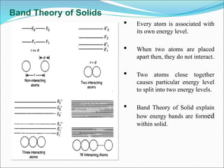
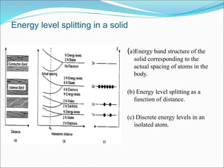
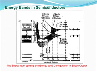
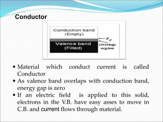
UNIT –IV
SEMICONDUCTOR PHYSICS
DEPARTMENT OF APPLIED
PHYSICS
Band Theory of Solids
• Every atom is associated with
its own energy level.
• When two atoms are placed
apart then, they do not interact.
• Two atoms close together
causes particular energy level
to split into two energy levels.
• Band Theory of Solid explain
how energy bands are formed
within solid.
Energy level splitting in a solid
(a)Energy band structure of the
solid corresponding to the
actual spacing of atoms in the
body.
(b) Energy level splitting as a
function of distance.
(c) Discrete energy levels in an
isolated atom.
Energy Bands in Semiconductors
The Energy level splitting and Energy band Configuration In Silicon Crystal
Valence Band:
• “The band formed by series of energy levels containing valence electron is
called Valence Band”.
• It may be completely filled or partially filled with electrons.
Conduction Band:
• “The Band formed by energy values of free electron that have broken their
covalent bonds is called Conduction band”.
• Conduction band is the next permitted energy band.
• It may be empty or partially filled with electrons.
Forbidden energy Gap
• The energy gap between the valence band and conduction band is called the
Forbidden energy gap or Forbidden Band or Band gap.
• This band is formed by series of non permitted energy levels above the top of
valence band and below the bottom of conduction band.
• Energy gap is denoted by Eg and it is the amount of energy supplied, to excite
the electron from valence band to conduction band. It is measured in eV.
Classification of solid: On the basis of energy band diagram
• Material which do not conduct current is called insulator.
• C.B. and V.B. separates with large energy gap, which is greater than
5 eV.
Insulator
Semiconductor
 Materials which have conductivity lies between
insulator and conductor are called
Semiconductor.
 Energy gap is small and it is of the order of 1eV.
Conductor
 Material which conduct current is called
Conductor
 As valence band overlaps with conduction band,
energy gap is zero
 If an electric field is applied to this solid,
electrons in the V.B. have easy asses to move in
C.B. and current flows through material.
Types of Semiconductor
 Intrinsic Semiconductor: Chemically pure
semiconductor is called Intrinsic Semiconductor.
 Extrinsic Semiconductor: Semiconductor doped
with some external impurity are called Extrinsic
semiconductor.
 Doping: It is the Process of adding impurities into
an intrinsic semiconductor .
Intrinsic Semiconductor(Si):
 Fig. A- Two dimensional representation of Si crystal
 Fig. B- The Band Structure View
Fig. A Fig. B
N-type Semiconductor:
Two dimensional representation The Band Structure View
 Semiconductors doped with pentavalent impurity (P,As)
are called N-type semiconductor.
 As pentavalent impurity atom donate free electrons it is
called Donor impurity.
 Donor impurities “create” an energy level, close to the
conduction band & represented by ED .
P-type Semiconductor:
Two dimensional representation The Band Structure View
 Semiconductors doped with trivalent impurity (Al, B) are
called P-type semiconductor.
 As trivalent impurity accept free electrons, so we call them
Acceptors.
 Acceptor impurities “create” discrete energy level, close to
the valence band & represented by EA .
Concept of Holes:
 Hole is nothing but the absence of electron.
 “Deficiency” of negative charge can be treated as a
positive charge.
 Holes are positive charge carriers. Movement of electrons
from nearby sites gives rise to movement of holes in
apposite direction.
 Hole is just like a bubble in liquid.
Fermi level & Fermi Energy
 For conductor: The highest occupied energy level
at 0ok is called Fermi level and the Energy
corresponding to it is called the Fermi Energy.
 For semiconductor: Fermi level is the reference
energy level and it correspond to the center of
gravity of conduction electron and valence hole.
Fermi-Dirac Distribution Function
)
exp(
1
1
)
(
kT
E
E
E
f
F



• f(E) is the function that gives the probability that particular
energy level having energy E is occupied by an electron at
Temperature T0 Kelvin. Where EF is the Fermi energy, k is
Boltzmann's constant.
• For conductor: The highest occupied energy level at 0K is
called Fermi level and the Energy corresponding to it is called
the Fermi Energy.
• For semiconductor: Fermi level is the reference energy
level and it correspond to the center of gravity of conduction
electron and valence hole.
Effect of temperature on Fermi Function
The above diagram represents variation of f(E) as a function of temperature.
All the curves pass through cross-over point C corresponding to f(E) =1/2.
Fermi level in Intrinsic semiconductor
 At T=0K the number of electrons in conduction band equals
the number of holes in valence band, ne = nh = ni .
Fermi level lies in the middle of the band gap.
 At T≠ 0 K, it depends upon the effective mass of electron
and hole.
*
*
g
ln
4
3
2 h
e
f
m
m
kT
E
E 









m*h>m*e
Temperature
Energy
Valence band
Conduction band
m*h = m*e
m*h < m*e
Fermi level in p-type semiconductor
 The number of holes in valence band are greater
than number of electrons in conduction band, nh > ne
 So the Fermi level shift towards the valence band.
 With temperature fermi level shifts towards Efi .,
Energy Band Diagram of n-type semiconductor at 0K and 300K
Fermi level in n-type semiconductor
 The number of electrons in conduction band are
greater than number of holes in valence band, ne > nh
 So the Fermi level shift towards the conduction band .
 With temperature Fermi level shifts towards the EFi
Energy Band Diagram of p-type semiconductor at 0K and 300K
Variation of Fermi level with impurity
concentration in n-type semiconductor:
Fig. (a): At low impurity concentration
Fig. (b): At moderate impurity concentration
Fig. (c): At high impurity concentration
Eg
Eg
Eg
Conduction band Conduction band
Valence band Valence band Valence band
ED
EF
EC
EV
E
Impurity Concentration
Fig: (a) Fig: (b) Fig: (c)
Eg
Conduction band
Drift Current
 Drift current: The current due to (motion) drifting of
charge carrier under application of electric field is
called Drift Current.
 Drift current density is given by
Where are the constants called mobility
of electrons and holes respectively.
h
e 
 ,
E
e
n
drift
e e
J 

)
(
E
e
p
drift
h h
J 

)
(
)
(
)
(
)
( drift
J
drift
J
drift h
e
J 

Diffusion current
 Diffusion current: The directional movement of charge
carriers due to concentration gradient is called Diffusion
Current.
 Diffusion current density due to electron is given by
 Diffusion current density due to hole is given by
Where De and Dh are the diffusion coefficient for electron and
hole respectively.
dx
dn
e
diffusion
e D
e
J 
)
(
dx
dp
h
diffusion
h D
e
J 

)
(
)
(
)
(
)
( diffusion
J
diffusion
J
diffusion h
e
J 

Conductivity of semiconductor
 Conductivity of intrinsic semiconductor:
σi = ni e( μe + μh)
 Conductivity of Extrinsic semiconductor:
For n – type semiconductor:
σn = n e μe = ND e μe
For p – type semiconductor:
σp = p e μh = NA e μh
Where ND and NA are the concentration of donor and
acceptor impurity.
p – n junction Diode
 The diode is just like a current valve.
 It allows unidirectional flow of current.
 Diode conduct only when it is in forward bias and do not
conduct ideally in reverse bias.
 It is used in rectifiers.
 Diode has a nonlinear voltage - current characteristics.
Formation of p-n Junction Diode
• Holes are the majority charge carriers and electrons are
the minority charge carriers in p- region.
• Electrons are the majority charge carriers and holes are
the minority charge carriers in n- region.
• p-n junction is the boundary between p-type and n-type
semiconductor.
Physical Structure and Symbol
Physical structure Diode circuit symbol
Biasing of p-n junction diode
Biasing of diode: Terminals of external battery is
connected to the terminals of diode is called as
biasing of diode.
 Forward Biasing: p terminal of diode is connected to
+ve and n terminal is connected to –ve terminal of
battery.
 Reverse Biasing: n terminal of diode is connected to
+ve and p terminal is connected to –ve terminal of
battery.
Energy Band Diagram of p-n junction diode
At equilibrium mode
In Forward Bias mode
Energy of
holes
Energy of
electron
In Reverse Bias mode.
Energy of
holes
Energy of
electron
Energy of
electron Energy of
holes
V-I Characteristics
The V-I Characteristics of p-n Junction diode.
http://www.bellsystemmemorial.com/belllabs_transistor.html
Pictorial History of Transistors
Transistor = Trans + resistor
 The transistor can be thought as a device in which
current travels from low resistance to high resistance
path.
Bipolar Junction Transistor
1. Common base mode
2. Common emitter mode
3. Common collector mode
 For efficient action of a transistor,
emitter- base junction is forward biased
and collector is reverse biased.
Modes of operation of Transistor
Energy band Diagram of a transistor
n-p-n Transistor in unbiased mode
Energy of
electrons
Energy of
holes
n-p-n Transistor in Common Base mode
Energy of
electrons
Energy of
holes
 When a current carrying conductor is placed in a
transverse magnetic field, a potential difference is
generated in the direction perpendicular to both the
current and the magnetic field, the voltage developed is
known as Hall voltage VH and the effect is known as Hall
effect.
I
B
v
B
F
Lorentz Force
F= -eBVd
d
I
e
-
+
VH
-
The Hall Effect: Discovered in 1897 by Edwin
H. Hall
Application of Hall Effect
 Determination of the “type of semiconductor”
 Determination of the “concentration” of charge
carrier (p or n).
 Determination of the “mobility” of charge
carrier (µ).
 Measurement of “magnetic field” (B).
 Measurement of “Hall coefficient” (RH).
THANK YOU

PPT.ppt

  • 1.
  • 2.
    Band Theory ofSolids • Every atom is associated with its own energy level. • When two atoms are placed apart then, they do not interact. • Two atoms close together causes particular energy level to split into two energy levels. • Band Theory of Solid explain how energy bands are formed within solid.
  • 3.
    Energy level splittingin a solid (a)Energy band structure of the solid corresponding to the actual spacing of atoms in the body. (b) Energy level splitting as a function of distance. (c) Discrete energy levels in an isolated atom.
  • 4.
    Energy Bands inSemiconductors The Energy level splitting and Energy band Configuration In Silicon Crystal
  • 5.
    Valence Band: • “Theband formed by series of energy levels containing valence electron is called Valence Band”. • It may be completely filled or partially filled with electrons. Conduction Band: • “The Band formed by energy values of free electron that have broken their covalent bonds is called Conduction band”. • Conduction band is the next permitted energy band. • It may be empty or partially filled with electrons.
  • 6.
    Forbidden energy Gap •The energy gap between the valence band and conduction band is called the Forbidden energy gap or Forbidden Band or Band gap. • This band is formed by series of non permitted energy levels above the top of valence band and below the bottom of conduction band. • Energy gap is denoted by Eg and it is the amount of energy supplied, to excite the electron from valence band to conduction band. It is measured in eV.
  • 7.
    Classification of solid:On the basis of energy band diagram • Material which do not conduct current is called insulator. • C.B. and V.B. separates with large energy gap, which is greater than 5 eV. Insulator
  • 8.
    Semiconductor  Materials whichhave conductivity lies between insulator and conductor are called Semiconductor.  Energy gap is small and it is of the order of 1eV.
  • 9.
    Conductor  Material whichconduct current is called Conductor  As valence band overlaps with conduction band, energy gap is zero  If an electric field is applied to this solid, electrons in the V.B. have easy asses to move in C.B. and current flows through material.
  • 10.
    Types of Semiconductor Intrinsic Semiconductor: Chemically pure semiconductor is called Intrinsic Semiconductor.  Extrinsic Semiconductor: Semiconductor doped with some external impurity are called Extrinsic semiconductor.  Doping: It is the Process of adding impurities into an intrinsic semiconductor .
  • 11.
    Intrinsic Semiconductor(Si):  Fig.A- Two dimensional representation of Si crystal  Fig. B- The Band Structure View Fig. A Fig. B
  • 12.
    N-type Semiconductor: Two dimensionalrepresentation The Band Structure View  Semiconductors doped with pentavalent impurity (P,As) are called N-type semiconductor.  As pentavalent impurity atom donate free electrons it is called Donor impurity.  Donor impurities “create” an energy level, close to the conduction band & represented by ED .
  • 13.
    P-type Semiconductor: Two dimensionalrepresentation The Band Structure View  Semiconductors doped with trivalent impurity (Al, B) are called P-type semiconductor.  As trivalent impurity accept free electrons, so we call them Acceptors.  Acceptor impurities “create” discrete energy level, close to the valence band & represented by EA .
  • 14.
    Concept of Holes: Hole is nothing but the absence of electron.  “Deficiency” of negative charge can be treated as a positive charge.  Holes are positive charge carriers. Movement of electrons from nearby sites gives rise to movement of holes in apposite direction.  Hole is just like a bubble in liquid.
  • 15.
    Fermi level &Fermi Energy  For conductor: The highest occupied energy level at 0ok is called Fermi level and the Energy corresponding to it is called the Fermi Energy.  For semiconductor: Fermi level is the reference energy level and it correspond to the center of gravity of conduction electron and valence hole.
  • 16.
    Fermi-Dirac Distribution Function ) exp( 1 1 ) ( kT E E E f F    •f(E) is the function that gives the probability that particular energy level having energy E is occupied by an electron at Temperature T0 Kelvin. Where EF is the Fermi energy, k is Boltzmann's constant. • For conductor: The highest occupied energy level at 0K is called Fermi level and the Energy corresponding to it is called the Fermi Energy. • For semiconductor: Fermi level is the reference energy level and it correspond to the center of gravity of conduction electron and valence hole.
  • 17.
    Effect of temperatureon Fermi Function The above diagram represents variation of f(E) as a function of temperature. All the curves pass through cross-over point C corresponding to f(E) =1/2.
  • 18.
    Fermi level inIntrinsic semiconductor  At T=0K the number of electrons in conduction band equals the number of holes in valence band, ne = nh = ni . Fermi level lies in the middle of the band gap.  At T≠ 0 K, it depends upon the effective mass of electron and hole. * * g ln 4 3 2 h e f m m kT E E           m*h>m*e Temperature Energy Valence band Conduction band m*h = m*e m*h < m*e
  • 19.
    Fermi level inp-type semiconductor  The number of holes in valence band are greater than number of electrons in conduction band, nh > ne  So the Fermi level shift towards the valence band.  With temperature fermi level shifts towards Efi ., Energy Band Diagram of n-type semiconductor at 0K and 300K
  • 20.
    Fermi level inn-type semiconductor  The number of electrons in conduction band are greater than number of holes in valence band, ne > nh  So the Fermi level shift towards the conduction band .  With temperature Fermi level shifts towards the EFi Energy Band Diagram of p-type semiconductor at 0K and 300K
  • 21.
    Variation of Fermilevel with impurity concentration in n-type semiconductor: Fig. (a): At low impurity concentration Fig. (b): At moderate impurity concentration Fig. (c): At high impurity concentration Eg Eg Eg Conduction band Conduction band Valence band Valence band Valence band ED EF EC EV E Impurity Concentration Fig: (a) Fig: (b) Fig: (c) Eg Conduction band
  • 22.
    Drift Current  Driftcurrent: The current due to (motion) drifting of charge carrier under application of electric field is called Drift Current.  Drift current density is given by Where are the constants called mobility of electrons and holes respectively. h e   , E e n drift e e J   ) ( E e p drift h h J   ) ( ) ( ) ( ) ( drift J drift J drift h e J  
  • 23.
    Diffusion current  Diffusioncurrent: The directional movement of charge carriers due to concentration gradient is called Diffusion Current.  Diffusion current density due to electron is given by  Diffusion current density due to hole is given by Where De and Dh are the diffusion coefficient for electron and hole respectively. dx dn e diffusion e D e J  ) ( dx dp h diffusion h D e J   ) ( ) ( ) ( ) ( diffusion J diffusion J diffusion h e J  
  • 24.
    Conductivity of semiconductor Conductivity of intrinsic semiconductor: σi = ni e( μe + μh)  Conductivity of Extrinsic semiconductor: For n – type semiconductor: σn = n e μe = ND e μe For p – type semiconductor: σp = p e μh = NA e μh Where ND and NA are the concentration of donor and acceptor impurity.
  • 25.
    p – njunction Diode  The diode is just like a current valve.  It allows unidirectional flow of current.  Diode conduct only when it is in forward bias and do not conduct ideally in reverse bias.  It is used in rectifiers.  Diode has a nonlinear voltage - current characteristics.
  • 26.
    Formation of p-nJunction Diode • Holes are the majority charge carriers and electrons are the minority charge carriers in p- region. • Electrons are the majority charge carriers and holes are the minority charge carriers in n- region. • p-n junction is the boundary between p-type and n-type semiconductor.
  • 27.
    Physical Structure andSymbol Physical structure Diode circuit symbol
  • 28.
    Biasing of p-njunction diode Biasing of diode: Terminals of external battery is connected to the terminals of diode is called as biasing of diode.  Forward Biasing: p terminal of diode is connected to +ve and n terminal is connected to –ve terminal of battery.  Reverse Biasing: n terminal of diode is connected to +ve and p terminal is connected to –ve terminal of battery.
  • 29.
    Energy Band Diagramof p-n junction diode At equilibrium mode
  • 30.
    In Forward Biasmode Energy of holes Energy of electron
  • 31.
    In Reverse Biasmode. Energy of holes Energy of electron Energy of electron Energy of holes
  • 32.
    V-I Characteristics The V-ICharacteristics of p-n Junction diode.
  • 33.
  • 34.
    Transistor = Trans+ resistor  The transistor can be thought as a device in which current travels from low resistance to high resistance path. Bipolar Junction Transistor
  • 35.
    1. Common basemode 2. Common emitter mode 3. Common collector mode  For efficient action of a transistor, emitter- base junction is forward biased and collector is reverse biased. Modes of operation of Transistor
  • 36.
    Energy band Diagramof a transistor n-p-n Transistor in unbiased mode Energy of electrons Energy of holes
  • 37.
    n-p-n Transistor inCommon Base mode Energy of electrons Energy of holes
  • 38.
     When acurrent carrying conductor is placed in a transverse magnetic field, a potential difference is generated in the direction perpendicular to both the current and the magnetic field, the voltage developed is known as Hall voltage VH and the effect is known as Hall effect. I B v B F Lorentz Force F= -eBVd d I e - + VH - The Hall Effect: Discovered in 1897 by Edwin H. Hall
  • 39.
    Application of HallEffect  Determination of the “type of semiconductor”  Determination of the “concentration” of charge carrier (p or n).  Determination of the “mobility” of charge carrier (µ).  Measurement of “magnetic field” (B).  Measurement of “Hall coefficient” (RH).
  • 40.