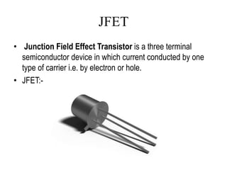
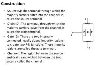
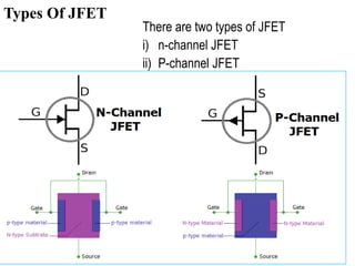
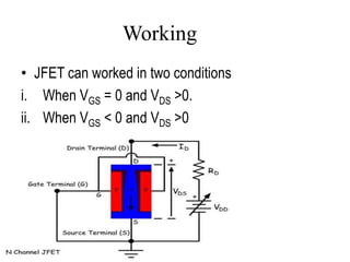
Junction Field Effect Transistor
(JFET)
By – Ateeb Khan (S.Y. B.Tech)
Content
• Field Effect transistor (FET)
• Junction Field Effect Transistor ( JFET)
• Construction of JFET
• Working of JFET
Introduction
The ordinary or bipolar transistor has two main
disadvantage.
• It has a low input impedance.
• It has considerable noise level.
To overcome this problem Field effect transistor (FET)
is introduced because of its:
• High input impedance
• Low noise level than ordinary transistor
• Field Effect Transistor is the voltage
controlled device.
JFET
MESFET
MISFET
MOSFET
JFET
• Junction Field Effect Transistor is a three terminal
semiconductor device in which current conducted by one
type of carrier i.e. by electron or hole.
• JFET:-
Construction
• Source (S): The terminal through which the
majority carriers enter into the channel, is
called the source terminal .
• Drain (D): The terminal, through which the
majority carriers leave from the channel, is
called the drain terminal .
• Gate (G): There are two internally
connected heavily doped impurity regions
to create two P-N junctions. These impurity
regions are called the gate terminal .
• Channel : The region between the source
and drain, sandwiched between the two
gates is called the channel .
Types Of JFET
There are two types of JFET
i) n-channel JFET
ii) P-channel JFET
Working
• JFET can worked in two conditions
i. When VGS = 0 and VDS >0.
ii. When VGS < 0 and VDS >0
Mathematical model
• The current in N-JFET due to a small
voltage VDS (that is, in the linear ohmic
region) is given by treating the channel
as a rectangular bar of material
of electrical conductivity.
ID = bW . qNDµnVDS
L
•where
•ID = drain–source current
•b = channel thickness for a
given gate voltage
•W = channel width
•L = channel length
•q = electron charge = 1.6 x
10−19 C
•μn = electron mobility
•Nd = n-type doping (donor)
concentration.
•VP = pinch-off voltage.
Linear region
• In Terms of IDSS
Channel Thickness
Constantcurrentregion
Junction Field Effect Transistor

Junction Field Effect Transistor

  • 1.
    Junction Field EffectTransistor (JFET) By – Ateeb Khan (S.Y. B.Tech)
  • 2.
    Content • Field Effecttransistor (FET) • Junction Field Effect Transistor ( JFET) • Construction of JFET • Working of JFET
  • 3.
    Introduction The ordinary orbipolar transistor has two main disadvantage. • It has a low input impedance. • It has considerable noise level. To overcome this problem Field effect transistor (FET) is introduced because of its: • High input impedance • Low noise level than ordinary transistor
  • 4.
    • Field EffectTransistor is the voltage controlled device. JFET MESFET MISFET MOSFET
  • 5.
    JFET • Junction FieldEffect Transistor is a three terminal semiconductor device in which current conducted by one type of carrier i.e. by electron or hole. • JFET:-
  • 6.
    Construction • Source (S):The terminal through which the majority carriers enter into the channel, is called the source terminal . • Drain (D): The terminal, through which the majority carriers leave from the channel, is called the drain terminal . • Gate (G): There are two internally connected heavily doped impurity regions to create two P-N junctions. These impurity regions are called the gate terminal . • Channel : The region between the source and drain, sandwiched between the two gates is called the channel .
  • 7.
    Types Of JFET Thereare two types of JFET i) n-channel JFET ii) P-channel JFET
  • 8.
    Working • JFET canworked in two conditions i. When VGS = 0 and VDS >0. ii. When VGS < 0 and VDS >0
  • 11.
    Mathematical model • Thecurrent in N-JFET due to a small voltage VDS (that is, in the linear ohmic region) is given by treating the channel as a rectangular bar of material of electrical conductivity. ID = bW . qNDµnVDS L •where •ID = drain–source current •b = channel thickness for a given gate voltage •W = channel width •L = channel length •q = electron charge = 1.6 x 10⁻¹⁹ C •μn = electron mobility •Nd = n-type doping (donor) concentration. •VP = pinch-off voltage.
  • 12.
  • 13.