Download to read offline
![1
Syllabus
Unit 6. Field Effect Transistor: (8 hours); [Ref. 2: Chapters. 15 & 16, Ref. 3,
Ref. 4: Chapter. 4]
JFET- Basic construction - Theory of operation - Static characteristics - Drain
characteristics- Advantages - MOSFET – Depletion enhancement MOSFET –
Construction – Static characteristics.Uni-junction Transistor - Construction-
operation Silicon Controlled rectifier - Construction biasing - operation-
applications.
Books forstudy:
1. Basic electronics- Santiram Kal
2. Basic electronics- B. L. Theraja
3. Principles of electronics- V. K. Mehta
4. A first coursein Electronics- Anwar A. Khan, Kanchan K. Dey
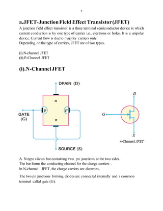
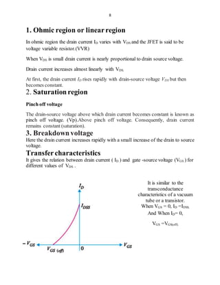
1.FET-FieldEffect Transistor
FET is an acronym for Field Effect Transistor.
It is a three- terminal unipolar solid state device like bipolar junction transistor
(BJT).
In FET current is controlled by an electric field setup in the device,
hence the name FET.
Here the current conduction is only by majority carriers. Due to electrons or holes
So FET is called a unipolar device.
The three terminal are :- (i).SOURCE (ii).DRAIN (iii).GATE
FET is a voltage controlled device.
Classificationof FET
Based on construction, there are two basic types of FET.
(a). JFET-Junction Field Effect Transistor
(b). MOSFET-Metal Oxide SemiconductorField Effect Transistor .
It is also called insulated gate FET- (IGFET)](https://image.slidesharecdn.com/jfet-200331113335/85/JFET-1-320.jpg)
![1
Syllabus
Unit 6. Field Effect Transistor: (8 hours); [Ref. 2: Chapters. 15 & 16, Ref. 3,
Ref. 4: Chapter. 4]
JFET- Basic construction - Theory of operation - Static characteristics - Drain
characteristics- Advantages - MOSFET – Depletion enhancement MOSFET –
Construction – Static characteristics.Uni-junction Transistor - Construction-
operation Silicon Controlled rectifier - Construction biasing - operation-
applications.
Books forstudy:
1. Basic electronics- Santiram Kal
2. Basic electronics- B. L. Theraja
3. Principles of electronics- V. K. Mehta
4. A first coursein Electronics- Anwar A. Khan, Kanchan K. Dey
1.FET-FieldEffect Transistor
FET is an acronym for Field Effect Transistor.
It is a three- terminal unipolar solid state device like bipolar junction transistor
(BJT).
In FET current is controlled by an electric field setup in the device,
hence the name FET.
Here the current conduction is only by majority carriers. Due to electrons or holes
So FET is called a unipolar device.
The three terminal are :- (i).SOURCE (ii).DRAIN (iii).GATE
FET is a voltage controlled device.
Classificationof FET
Based on construction, there are two basic types of FET.
(a). JFET-Junction Field Effect Transistor
(b). MOSFET-Metal Oxide SemiconductorField Effect Transistor .
It is also called insulated gate FET- (IGFET)](https://image.slidesharecdn.com/jfet-200331113335/75/JFET-1-2048.jpg)


The document summarizes key aspects of field effect transistors (FETs). It describes the basic construction and operation of junction FETs (JFETs) and metal-oxide-semiconductor FETs (MOSFETs). It explains that FETs use an electric field to control the flow of majority carriers through a channel. The document also provides JFET characteristics curves and defines different operating regions like ohmic, saturation and breakdown. It compares FETs to bipolar junction transistors (BJTs) and lists some common applications of JFETs in electronics.


![Aim-to study characterstics of fet (field effect [Autosaved].pptx](https://cdn.slidesharecdn.com/ss_thumbnails/aim-tostudycharactersticsoffetfieldeffectautosaved-221113041420-4dcee974-thumbnail.jpg?width=640&height=640&fit=bounds)


