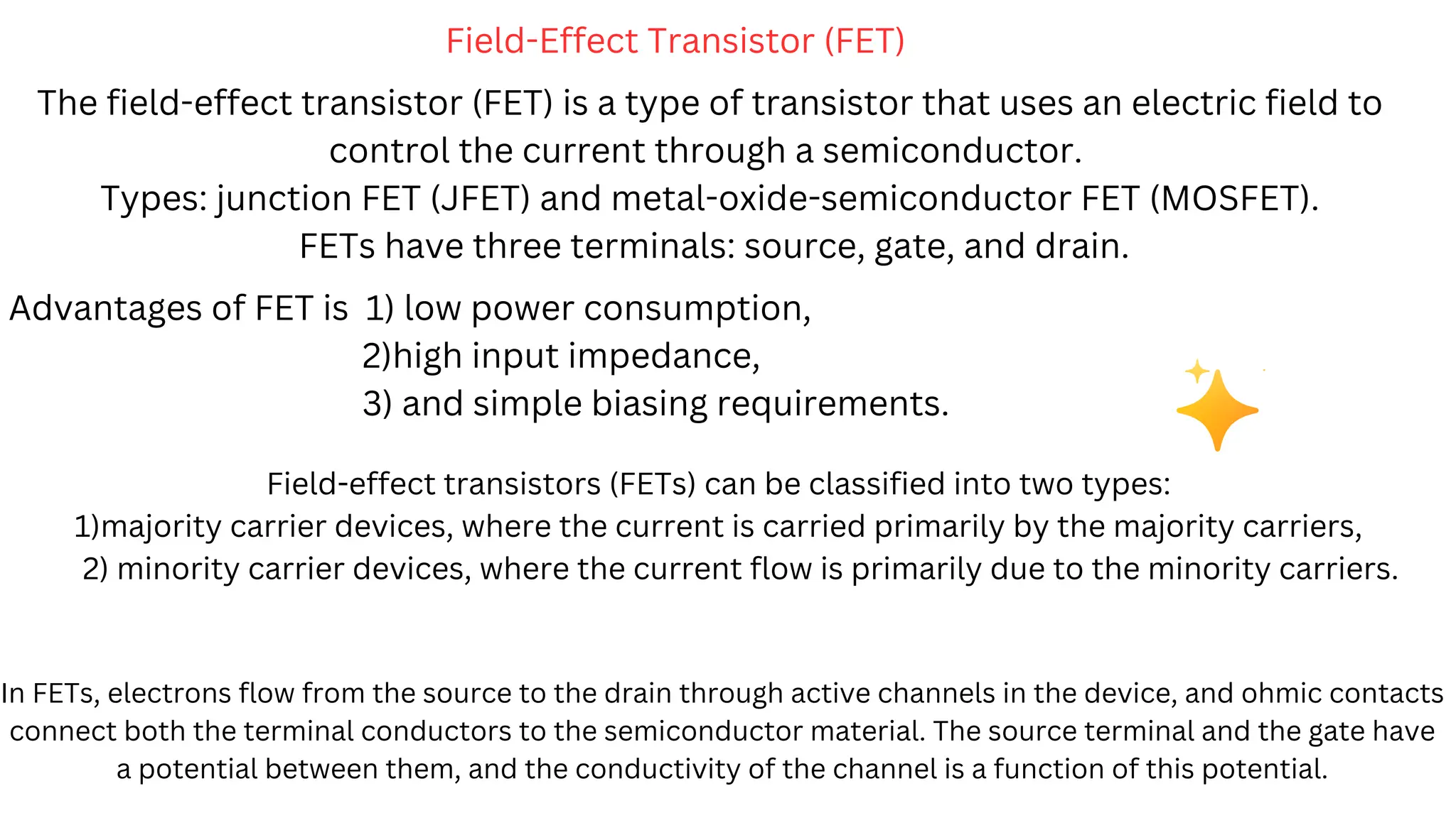
The field-effect transistor(FET) is a type of transistor that uses an electric field to
control the current through a semiconductor.
Types: junction FET (JFET) and metal-oxide-semiconductor FET (MOSFET).
FETs have three terminals: source, gate, and drain.
Field-Effect Transistor (FET)
Advantages of FET is 1) low power consumption,
2)high input impedance,
3) and simple biasing requirements.
Field-effect transistors (FETs) can be classified into two types:
1)majority carrier devices, where the current is carried primarily by the majority carriers,
2) minority carrier devices, where the current flow is primarily due to the minority carriers.
In FETs, electrons flow from the source to the drain through active channels in the device, and ohmic contacts
connect both the terminal conductors to the semiconductor material. The source terminal and the gate have
a potential between them, and the conductivity of the channel is a function of this potential.
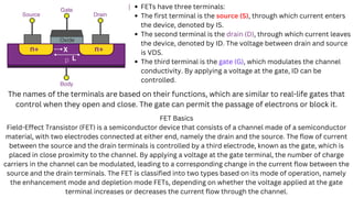
2.
FETs have threeterminals:
The first terminal is the source (S), through which current enters
the device, denoted by IS.
The second terminal is the drain (D), through which current leaves
the device, denoted by ID. The voltage between drain and source
is VDS.
The third terminal is the gate (G), which modulates the channel
conductivity. By applying a voltage at the gate, ID can be
controlled.
The names of the terminals are based on their functions, which are similar to real-life gates that
control when they open and close. The gate can permit the passage of electrons or block it.
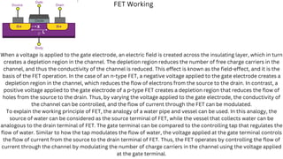
FET Basics
Field-Effect Transistor (FET) is a semiconductor device that consists of a channel made of a semiconductor
material, with two electrodes connected at either end, namely the drain and the source. The flow of current
between the source and the drain terminals is controlled by a third electrode, known as the gate, which is
placed in close proximity to the channel. By applying a voltage at the gate terminal, the number of charge
carriers in the channel can be modulated, leading to a corresponding change in the current flow between the
source and the drain terminals. The FET is classified into two types based on its mode of operation, namely
the enhancement mode and depletion mode FETs, depending on whether the voltage applied at the gate
terminal increases or decreases the current flow through the channel.
3.
When a voltageis applied to the gate electrode, an electric field is created across the insulating layer, which in turn
creates a depletion region in the channel. The depletion region reduces the number of free charge carriers in the
channel, and thus the conductivity of the channel is reduced. This effect is known as the field-effect, and it is the
basis of the FET operation. In the case of an n-type FET, a negative voltage applied to the gate electrode creates a
depletion region in the channel, which reduces the flow of electrons from the source to the drain. In contrast, a
positive voltage applied to the gate electrode of a p-type FET creates a depletion region that reduces the flow of
holes from the source to the drain. Thus, by varying the voltage applied to the gate electrode, the conductivity of
the channel can be controlled, and the flow of current through the FET can be modulated.
To explain the working principle of FET, the analogy of a water pipe and vessel can be used. In this analogy, the
source of water can be considered as the source terminal of FET, while the vessel that collects water can be
analogous to the drain terminal of FET. The gate terminal can be compared to the controlling tap that regulates the
flow of water. Similar to how the tap modulates the flow of water, the voltage applied at the gate terminal controls
the flow of current from the source to the drain terminal of FET. Thus, the FET operates by controlling the flow of
current through the channel by modulating the number of charge carriers in the channel using the voltage applied
at the gate terminal.
FET Working
4.
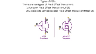
Types of FETs
Thereare two types of Field Effect Transistors:
1)Junction Field Effect Transistor (JFET)
2)Metal oxide semiconductor Field Effect Transistor (MOSFET)
5.
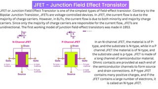
JFET or JunctionField Effect Transistor is one of the simplest types of field-effect transistor. Contrary to the
Bipolar Junction Transistor, JFETs are voltage-controlled devices. In JFET, the current flow is due to the
majority of charge carriers. However, in BJTs, the current flow is due to both minority and majority charge
carriers. Since only the majority of charge carriers are responsible for the current flow, JFETs are
unidirectional. The first working model of junction field-effect transistors was made in 1953.
In an N-channel JFET, the material is of P-
type, and the substrate is N-type, while in a P
channel JFET the material is of N-type, and
the substrate used is p-type. JFET is made of
a long channel of semiconductor material.
Ohmic contacts are provided at each end of
the semiconductor channels to form source
and drain connections. A P-type JFET
contains many positive charges, and if the
JFET contains a large number of electrons, it
is called an N-type JFET.
6.
JFET Operation
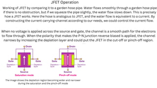
Working ofJFET by comparing it to a garden hose pipe. Water flows smoothly through a garden hose pipe
if there is no obstruction, but if we squeeze the pipe slightly, the water flow slows down. This is precisely
how a JFET works. Here the hose is analogous to JFET, and the water flow is equivalent to a current. By
constructing the current carrying-channel according to our needs, we could control the current flow.
When no voltage is applied across the source and gate, the channel is a smooth path for the electrons
to flow through. When the polarity that makes the P-N junction reverse biased is applied, the channel
narrows by increasing the depletion layer and could put the JFET in the cut-off or pinch-off region.
The image shows the depletion region becoming wider and narrower
during the saturation and the pinch-off mode
7.
JFET Types
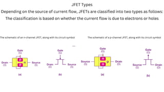
Depending onthe source of current flow, JFETs are classified into two types as follows:
The classification is based on whether the current flow is due to electrons or holes
The schematic of an n-channel JFET, along with its circuit symbol The schematic of a p-channel JFET, along with its circuit symbol
8.
Junction Field EffectTransistor Applications
JFET is used as a switch
JFET is used as a chopper
JFET is used as a buffer
JFETs are used in oscillatory circuits
JFETs are used in cascade amplifiers
JFET Advantages
JFET has a high impedance
JFETs are low power consumption devices
JFET can be fabricated in a smaller size,
(they occupy less space in circuits due to their smaller size.)
JFET Disadvantages
It has a low gain-bandwidth product
The performance of JFET is affected as frequency increases due to feedback by internal capacitance.
9.
Q1)What is JFET?
ANS:-JFET or Junction Field Effect Transistor is a unipolar current-controlled semiconductor
device with three terminals: source, drain, and gate. JFETs are commonly used as
switches and amplifiers.
Q2) When was the junction field-effect transistor invented?
ANS:-The first working model of junction field-effect transistors was made in 1953.
Q3How many diodes do junction field-effect transistors contain?
ANS:-The Junction Field-effect transistor contains two diodes.
Q4)List a difference between JFET and BJT.
ANS:-In BJT, the output current is controlled by the base current. In JFET, the output current
is controlled by the input voltage.
Q5)What is a JFET used for?
ANS:-JFET is used as a switch, buffer and chopper. They are also used in oscillatory circuits.


![Aim-to study characterstics of fet (field effect [Autosaved].pptx](https://cdn.slidesharecdn.com/ss_thumbnails/aim-tostudycharactersticsoffetfieldeffectautosaved-221113041420-4dcee974-thumbnail.jpg?width=640&height=640&fit=bounds)


