
Recommended
More Related Content
What's hot
What's hot (17)
Viewers also liked
Viewers also liked (16)
Similar to Ijaerv10n9spl 473
Similar to Ijaerv10n9spl 473 (20)
Recently uploaded
Recently uploaded (20)
Ijaerv10n9spl 473
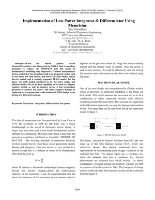
- 1. Implementation of Low Power Integrator & Differentiator Using Memristor 1 Joy Chowdhury PG Student, School of Electronics Engineering KIIT University, Bhubaneswar joychowdhury87@yahoo.in 2 J. K. Das, 3 N. K. Rout 2,3 Associate Professor School of Electronics Engineering KIIT University, Bhubaneswar jkdas12@gmail.com, nkrout@kiit.ac.in Abstract—When the fourth passive circuit element(Memristor) was discovered in 2008 it had tremendous potential to replace the MOSFETS and this made its mathematical modeling very imperative. Various mathematical device models for the memristor had been proposed earlier such as the linear ion drift model, non linear ion drift model, tunnel barrier model, and a recently proposed TEAM model. But the linear ion drift model continued to be the most simple and efficient model. Due to its dual capability to be used as a bipolar resistive switch as well as memory device it has tremendous potential to harness low power and more compact designs by replacing or in conjunction to the standard CMOS design styles giving new hybrid structures. Keywords- Memristor, Integrator, differentiator, low power INTRODUCTION The idea of memristors was first postulated by Leon Chua in 1970. Its invention in 2008 by HP Labs was a major breakthrough in the world of electronic circuit theory. A major leap was taken and a new fourth fundamental passive element was introduced. The basic idea struck Chua from the symmetry conditions exhibited in Aristotle's THEORY OF MATTER . The working principle of memristor basically revolves around the two most basic circuit parameters namely flux(φ) and charge(q). This new device is very similar to a resistor except that it is defined in terms of its Memristance (M) which is given as where M denotes a functional relationship between magnetic flux(φ) and electric charge(q).From the mathematical relations of the memristor it can be comprehended that the electrical resistance of the memristor is not constant rather it depends on the previous values of charge that was previously present and the present value of current. Thus the device is said to have memory. It could be effectively used for storing the previous state information or data bits even without using flip flops. MATHEMATICAL MODEL One of the most simple and computationally efficient models which is prevalent in memristor modeling is the linear ion drift model. This model assumes the memristor device to be a combination of series connected resistors with effective switching possible between them. This concept was supported in the fabrication process by varying the doping concentration of the . The stated fact can be seen from the hp lab memristor model in figure 1. Figure 1: HP Lab Memristor Model The device released by Stanley Williams from HP Labs was made up of thin film titanium dioxide (TiO2) which was selectively doped. The doping mentioned here was implemented by incorporating extra oxygen vacancies in the undoped thin film. The doped region has a resistance Ron while the undoped area has a resistance Roff. Several phenomenon are assumed here which include a) ohmic conductance , b) equal average ion mobility c)linear ion drift in presence of uniform electric field. The transport of charge carriers within the thin film titanium dioxide can be explained from the figure 2. International Journal of Applied Engineering Research ISSN 0973-4562 Volume 10, Number 9 (2015) © Research India Publications ::: http://www.ripublication.com 9009
- 2. Figure 2 : Transport of oxygen vacancies in TiO2 thin film. The relation between the derivative of the state variable and voltage is stated as where Ron is the resistance when w(t)= D and Roff is the resistance when w(t)= 0. To aid the linear ion drift model a window function is used to limit the movement of charge carriers within the device bounds. Similar to signal processing applications a window function is multiplied to the derivative of the state variable to nullify it. The ideal choice is rectangular window function. But due to the absence of any non linearity consideration several modifications to this window has been presented in . By far the best performance is demonstrated by the Prodromakis window which also ensure scalability of the window function by introducing a scalar multiplicative factor. APPLICATIONS The memristor serves as a bipolar resistive switch with history mechanisms. It can be used to substitute conventional electronic switches which are made of bipolar junction transistors or Mosfets. Sometimes they can be used as a substitute for resistors. They find extensive applications in neuromorphic systems and recently with the development of memcapacitance and meminductance they are a potential component of high frequency RF circuits. The most widely prevalent and commercial application of memristor is non volatile Random Access Memory which has already been developed by HP Labs. Crossbar latch memory is another widespread application which is expected to hit the market in the next two years. Minimal power consumption and very less die area are two of the most lucrative properties of the memristor which can be extensively dominated. In this paper we have tried to implement memristor based circuits for analog computation and instrumentation. The circuits by marked reduction in power consumption and hence better compactness and greater reliability. Also the fabrication of memristors is compatible with the existing CMOS technology. ANALOG CIRCUITS The Integrator and Differentiator: In this paper the analysis covers the integrator and the differentiator. This two circuits are widely used for linear wave shaping, analog computation, design of communication systems(transmitters and receivers) , data converters , spectral shaping and even data encryption. The integrating amplifier more commonly known as the integrator is a circuit in which gives the output waveform as the integral of the applied input voltage. Such as circuit can be achieved by using an opamp based inverting amplifier configuration in which a capacitor replaces the resistor in the feedback path. Figure 3 : Integrator circuit diagram with input and output waveform. From figure3 it is seen that since the inverting input is at virtual ground (1) (2) By applying Kirchhoff's current law at the inverting input we get (3) therefore, (4) or , (5) where ) is the constant of integration and its value is proportional to the value of output voltage at time t=0. International Journal of Applied Engineering Research ISSN 0973-4562 Volume 10, Number 9 (2015) © Research India Publications ::: http://www.ripublication.com 9010
- 3. The integrator is very widely used in analog computers, analog -to- digital converters (ADC) and signal - waveshaping circuits. The differentiating amplifier or the differentiator as implied from the name performs the mathematical operation of differentiation. The output waveform is given as the derivative of the applied input signal. This differentiator is constructed by from the basic inverting amplifier by interchanging the input resistor by a capacitor and the usual resistor in the feedback path. Figure 4 : Differentiator circuit Since the inverting input is at virtual ground, (6) (7) Then applying KCL at the inverting input we obtain, (7) therefore , (8) or, (9) Thus the output voltage is RC(time constant) times the negative instantaneous rate of change of the input voltage Vin with time. A triangular waveform at the input produces a square wave at the output. The differentiator is very widely used in waveshaping circuits for detecting high-frequency components in the input signal, also used as a 'rate-of-change' detector in FM modulators. RESULTS The opamp based circuits were simulated in cadence 180nm technology and transient analysis was run. Then the normal circuits were suitably modified to form the memristor based integrator and differentiator circuits. The on resistance of the memristor has to be adjusted in the modeling code to suit the RC time constant values. The transient analysis was run and the transient power was calculated for all the configurations. The power values are tabulated below. Figure 5: Output of normal integrator for square wave input Figure 6 : Transient Power Analysis of normal integrator Figure 7: Output response of memristor based integrator Figure 8: Transient power Analysis of Memristor based integrator Figure 9: Differentiator output for triangular wave input International Journal of Applied Engineering Research ISSN 0973-4562 Volume 10, Number 9 (2015) © Research India Publications ::: http://www.ripublication.com 9011
- 4. Figure 10: Transient Power analysis for normal differentiator Figure 11: Output response of memristor based differentiator for triangular wave input Figure 12: Transient Power analysis of memristor based differentiator. From the analysis of the above results we that in the memristor based circuits we obtain a greater power reduction which is in the nano watts range as compared to the normal opamp - resistor based circuits. The comparison in power is shown in the table below. The value of Ron in all cases is taken to be 500 ohms. Table 1 : Power comparison of the implemented designs Design Technology Device Length Transient Power (watts) Integrator CMOS OPAMP based L= 180nm × Integrator Memristor based D= 3nm 49.492 × 10⁻⁹ Differentiator CMOS OPAMP based L= 180nm 15.786 × 10⁻⁶ Differentiator Memristor based D=3nm 16.48 × 10⁻⁹ CONCLUSION Thus we can see that in case of the circuits implemented by memristors the power dissipation is very minimal and the leakage power is almost negligible as compared to the existing VLSI design styles. Also due to its extremely small device length it further enhances design integration and miniaturization. REFERENCES 1. Chua, L.O., ―Memristor- the missing circuit element‖ , IEEE Trans. Circuit Theory, 1971, vol. CT- 18, no. 5, pp. 507-519. 2. Chua, L.O. and Kang, S.M.. ―Memristive devices and systems‖ , Proceedings of the IEEE, 1976, vol. 64, no. 2, pp. 209-223. 3. Frank Y. Wang, "Memristor for introductory physics", arXiv:0808.0286vl [physics.class-ph] 4Aug2008. 4. S.Thakoor, A. Moopenn, T. Daud, and A.P. Thakoor, "Solid-state thin-film memistor for electronic neural networks", Journal of Applied Physics, vol. 67, March 15, 1990, pp. 3132-3135 5. C.Nagarajan and M.Madheswaran – „Analysis and Implementation of LLC-T Series Parallel Resonant Converter with Fuzzy controller‟- International Journal of Engineering Science and Technology (IJEST), Applied Power Electronics and Intelligent Motion Control. Vol.2 (10), pp 35-43, December 2010 6. Dimitri Strukov, Gregory Snider , Duncan Stewart , and Stanley Williams, "The missing memristor found", Nature. 7. Chris Yakopcic , "A Memristor Device Model", IEEE Electron Device Letters, Vol.32, No.10, Oct 2011. 8. Y. N. Joglekar and S. J. Wolf, “The Elusive memristor: Properties of basic electrical circuits,” Eur. J. Phys., vol. 30, no. 4, pp. 661–675, Jul. 2009. 9. Z. Biolek, D. Biolek, and V. Biolkova, “SPICE model of memristor with nonlinear dopant drift,” Radioengineering, vol. 18, no. 2, pp. 210–214, Jun. 2009. 10. C.Nagarajan and M.Madheswaran - „DSP Based Fuzzy Controller for Series Parallel Resonant converter‟- Springer, Frontiers of Electrical and Electronic Engineering, Vol. 7(4), pp. 438-446, Dec.12. 11. E. Lehtonen and M. Laiho, “CNN using memristors for neighborhood connections,” in Proc. Int. Workshop Cell. Nanoscale Netw. Their Appl., Feb. 2010, pp. 1–4. 12. J. G. Simmons, “Generalized formula for the electric tunnel effect between similar electrodes separated by a thin insulating film,” J. Appl. Phys., vol. 34, no. 6, pp. 1793–1803, Jan. 1963. 13. E. Lehtonen, J. Poikonen, M. Laiho, and W. Lu, “Time-dependency of the threshold voltage in memristive devices,” in Proc. IEEE Int. Symp. Circuits Syst., May 2011, pp. 2245–2248. 14. Shahar Kvatinsky, Eby G. Friedman, Avinoam Kolodny, "TEAM: ThreEshold Adaptive Memristor Model", IEEE Transactions on Circuits and Systems-I, vol.60, no.1, jan-2013. 15. M. D. Pickett, D. B. Strukov, J. L. Borghetti, J. J. Yang, G. S. Snider, D. R. Stewart, and R. S. Williams, “Switching dynamics in titanium dioxide memristive devices,” J. Appl. Phys., vol. 106, no. 7, pp. 1–6, Oct. 2009. International Journal of Applied Engineering Research ISSN 0973-4562 Volume 10, Number 9 (2015) © Research India Publications ::: http://www.ripublication.com 9012