1) The document proposes techniques for reducing power consumption in VLSI circuits, including minimizing bus transitions using coding schemes, resistive feedback paths to eliminate glitches, and voltage scaling.
2) A resistive feedback method is developed to eliminate glitches in CMOS circuits which reduces power consumption and improves performance.
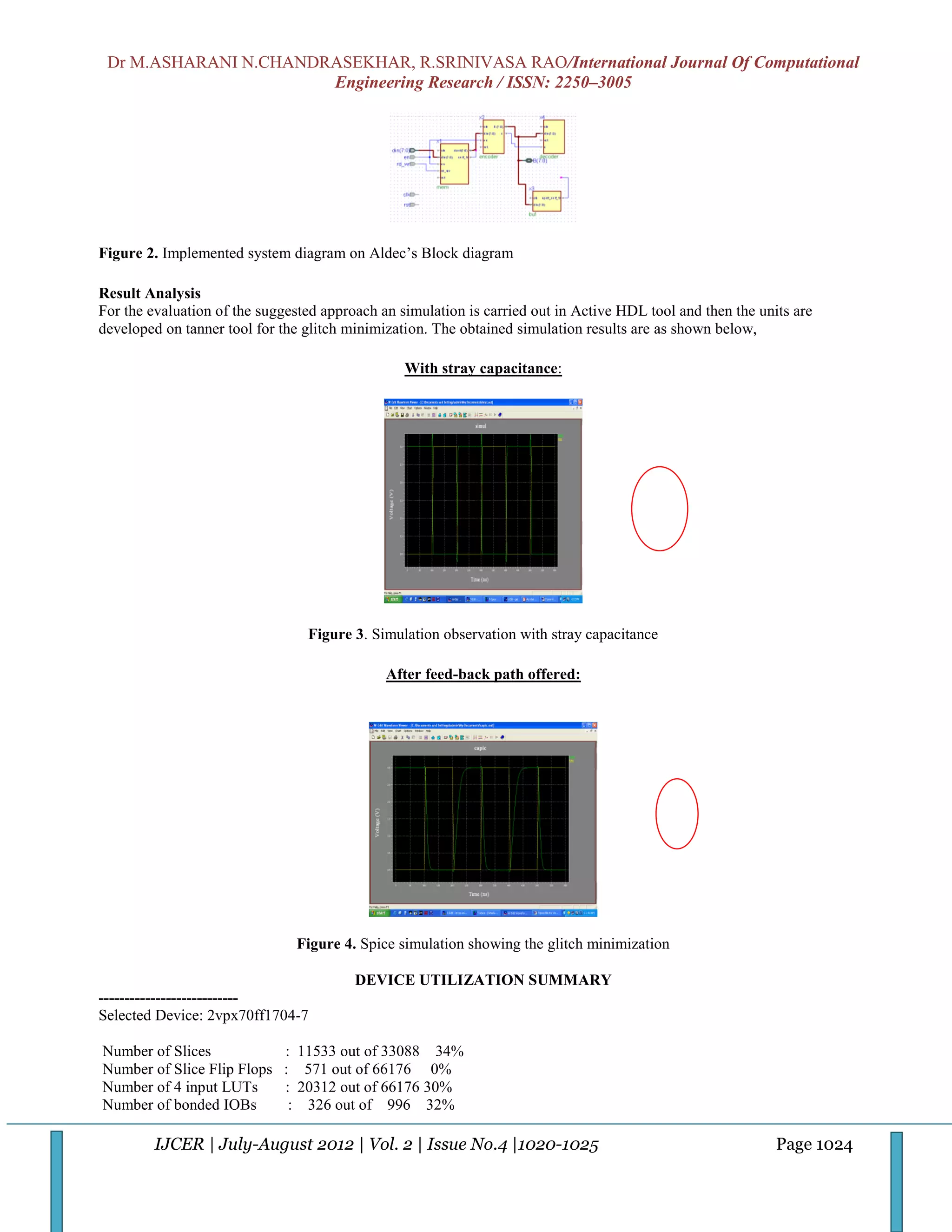
3) Simulation results show that the proposed resistive feedback technique is effective at minimizing glitches and reducing unnecessary power dissipation compared to a design without feedback paths.
IJRET : International Journal of Research in Engineering and Technology is an international peer reviewed, online journal published by eSAT Publishing House for the enhancement of research in various disciplines of Engineering and Technology. The aim and scope of the journal is to provide an academic medium and an important reference for the advancement and dissemination of research results that support high-level learning, teaching and research in the fields of Engineering and Technology. We bring together Scientists, Academician, Field Engineers, Scholars and Students of related fields of Engineering and Technology
Vlsi design process for low power design methodology using reconfigurable fpgaeSAT Publishing House
IJRET : International Journal of Research in Engineering and Technology is an international peer reviewed, online journal published by eSAT Publishing House for the enhancement of research in various disciplines of Engineering and Technology. The aim and scope of the journal is to provide an academic medium and an important reference for the advancement and dissemination of research results that support high-level learning, teaching and research in the fields of Engineering and Technology. We bring together Scientists, Academician, Field Engineers, Scholars and Students of related fields of Engineering and Technology.
With Increase in Portable devices, VLSI chips has to consider about Power usages in VLSI silicon chips. So Power Aware design and verification is so important in Industry. To get basic knowledge on Low Power Design and Verification with UPF basics Go through this Slides.
Note : To get more understanding Recommending to see first section - Low power in vlsi with upf basics part 1
With Increase in Portable devices, VLSI chips has to consider about Power usages in VLSI silicon chips. So Power Aware design and verification is so important in Industry. To get basic knowledge on Low Power Design and Verification with UPF basics Go through this Slides.
Design and Implementation of Refresh and Timing Controller Unit for LPDDR2 Me...Editor IJCATR
this paper presents a “Implementation of “Refresh And Timing Controller” unit for low power double data rate 2 memory
controller (LPDDR2 MEMORY CONTROLLER). “Refresh and Timing Controller” unit plays a vital role for LPDDR2 memory
controller .It maintains different timing parameters to handle various commands for memory like refresh, read and write operations and
also performs Memory Initialization. Since it is low power DDR2 the maximum duration in power-down mode and deep power down
mode is maintained by “Refresh and Timing Controller” unit. The refresh rate period is programmable using the Refresh Period
Register. It supports “All Bank Refresh”. The unit has timers to accommodate Refresh, Read/Write, and Power down modes. The RTL
is done using the System Verilog. The design is simulated
The demand for portable electronic devices that offers increase in functions, performance at lower costs and smaller sizes increased rapidly. Designing complex SOCs is a challenge, especially at 90 nanometers Technology, where new problems crop up - power efficiency is being the biggest of problems. For different modes we cannot design different operating circuits, better to have technique that will have minimum circuit changes and in all modes it will save power which is wasted. This paper provides some guidelines on how Low Power design using UPF approach can be introduced for a design.
Vlsi implementation of a programmable low drop out voltage regulatoreSAT Journals
Abstract LDO voltage regulators compose a small subset of the power supply arena. Low-drop-out (LDO) voltage regulators are used in analog applications that generally require low noise and high accuracy power rails. Voltage regulators provide a constant voltage supply rail under certain loading conditions. Circuits that are not performing tasks are temporarily turned off lowering the overall power consumption. The LDO voltage regulator, therefore, must respond quickly to system demands and power up connected circuits. To motivate new aspect of power management towards a design of a low drop-out voltage regulator that fulfils the present industry requirements as well as the upcoming demands of the future, it becomes necessary to design the LDO regulator which gives overall performance. A low-voltage low-dropout regulator that uses an Vdd of 1 V to an output of 0.8–0.74 V, with 32-nm CMOS technology is proposed. By scaling down the technology, we can get lower power consumption. More emphasis is given on the compactness and low drop-out voltage. The latest power management unit concept inside the system on chip (Soc) scheme inspires the digital control potential for the design of a novel LDO regulator. A simple operational transconductance amplifier is used as the error amplifier (EA), with a current splitting technique which is able to boost the gain. In the rail-to-rail output stage of the EA, a power noise cancellation mechanism is adopted. Programmability is added by applying two external control signals. These advantages allow the proposed LDO regulator to achieve a 60-mV output variation for low load transient, area efficient architecture with low power consumption. Keywords: low drop-out,32nm,low power consumption, programmability
International Journal of Engineering Research and DevelopmentIJERD Editor
Electrical, Electronics and Computer Engineering,
Information Engineering and Technology,
Mechanical, Industrial and Manufacturing Engineering,
Automation and Mechatronics Engineering,
Material and Chemical Engineering,
Civil and Architecture Engineering,
Biotechnology and Bio Engineering,
Environmental Engineering,
Petroleum and Mining Engineering,
Marine and Agriculture engineering,
Aerospace Engineering.
Low Power VLSI design architecture for EDA (Electronic Design Automation) and Modern Power Estimation, Reduction and Fixing technologies including clock gating and power gating
Power reduction techniques are important for the modern VLSI designs. Power is the today's major concern when we come to optimal trade off between area, performance and power.
ENERGY-EFFICIENT LOW DROPOUT REGULATOR WITH SWITCHING MECHANISM AND COURSE RE...ijesajournal
The proposed work presents an Energy-efficient, low dropout (LDO) regulator with switching mechanism reduces the energy consumption of IoT devices when the sensors are in idle time. Based on the analysis of IoT devices and sensors, modern power management designs for IoT demands for fully integrated solutions to decrease power consumption while maintaining the quick transient response to signal variations. LDO voltage regulators, as power management devices should adjust to modern technological and industrial trends. To increase the current capability with a minimum standby quiescent current under small-signal operation, the proposed work has a switching circuit acting as an ON and OFF switch. To reduce the dropout a course regulator and loop filter is added and circuit is enhanced for maximum reduced dropout. As a result, the efficiency gets increased.
A Novel Fuzzy Variable-Band Hysteresis Current Controller For Shunt Active Po...IDES Editor
This paper presents a novel fuzzy control scheme
applied to shunt active power filters for harmonic and reactive
power compensation. A TSK type fuzzy logic controller is
proposed for APF reference current generation. To control
the maximum switching frequency of the converter within
limit a novel fuzzy hysteresis band current controller is used.
The band height, based on fuzzy control principle is changed
with the value of supply voltage and slope of reference current
Analysis and design of single switch forward-flyback two-channel led driver w...LeMeniz Infotech
Analysis and design of single switch forward-flyback two-channel led driver with resonant-blocking capacitor
To Get this projects Call : 9566355386 / 99625 88976
Visit : www.lemenizinfotech.com / www.ieeemaster.com
Mail : projects@lemenizinfotech.com
Now day’s the power factor has become a major problem in power system to improve the power quality of the grid, as power factor is affected on the grid due to the nonlinear loads connected to it. Single phase bridgeless AC/DC power factor correction (PFC) topology to improve the power factor as well as the total harmonic distortion (THD) of the utility grid is proposed. By removing the input bridge in conventional PFC converters, the control circuit is simplified; the total harmonics distortion (THD) and power factor (PF) are improved. The PI controller operates in two loops one is the outer control loop which calculates the reference current through LC filter and signal processing. Inner current loop generates PWM switching signals through the PI controller. The output of the proposed PFC topology is verified for prototype using MATLAB circuit simulations. The experimental system is developed, and the simulation results are obtained.
IJCER (www.ijceronline.com) International Journal of computational Engineerin...ijceronline
Call for paper 2012, hard copy of Certificate, research paper publishing, where to publish research paper,
journal publishing, how to publish research paper, Call For research paper, international journal, publishing a paper, IJCER, journal of science and technology, how to get a research paper published, publishing a paper, publishing of journal, publishing of research paper, research and review articles, IJCER Journal, How to publish your research paper, publish research paper, open access engineering journal, Engineering journal, Mathematics journal, Physics journal, Chemistry journal, Computer Engineering, Computer Science journal, how to submit your paper, peer review journal, indexed journal, research and review articles, engineering journal, www.ijceronline.com, research journals,
yahoo journals, bing journals, International Journal of Computational Engineering Research, Google journals, hard copy of Certificate,
journal of engineering, online Submission
A phenomenology of human-electricity relationsJames Pierce
This paper investigates the philosophical question of how we can experience energy with the aim of informing the design of future ways of experiencing energy by means of technology. Four human-technology relations formulated by philosopher of technology Don Ihde are presented. Each is then developed in the context of electrical interactive technologies. In conclusion these human-electricity and human-technology relations are employed in order to interpret current work related to energy and sustainability within HCI and point to future work in these areas.
Welcome to International Journal of Engineering Research and Development (IJERD)IJERD Editor
journal publishing, how to publish research paper, Call For research paper, international journal, publishing a paper, IJERD, journal of science and technology, how to get a research paper published, publishing a paper, publishing of journal, publishing of research paper, reserach and review articles, IJERD Journal, How to publish your research paper, publish research paper, open access engineering journal, Engineering journal, Mathemetics journal, Physics journal, Chemistry journal, Computer Engineering, Computer Science journal, how to submit your paper, peer reviw journal, indexed journal, reserach and review articles, engineering journal, www.ijerd.com, research journals,
yahoo journals, bing journals, International Journal of Engineering Research and Development, google journals, hard copy of journal
A simple 10-cell RL-TL test circuit has been simulated using two completely different simulators: Microcap10 (MC10, evaluation version) and DWS. The first one is a classical Nodal Analysis Spice family simulator with a good model for Transmission Lines (TL). DWS (Digital Wave Simulator) is based on completely different DSP algorithms (Digital Wave Network equivalent)
Not our fault! - earth faults, past, present, and future, and their mitigationDennis Keen
This paper examines the technology development of different types of arc suppression coils, including dry and oil filled types. The tuning methods used including switched capacitances or reactance and moving coil types. How this method of earth fault protection compares with other methods and what options can be added to the arc suppression coil to improve the performance as an earth fault minimization system.
This paper also considers the wider electricity industry’s attitude to Arc Suppression Coils or Rapid Earth Fault Current Limiters (REFCL) and applications to safety including Earth Potential Rise (EPR) and induction effects. Mitigation of bush fires and forest fire risks and the use of REFCL’s in transmission and distribution systems up to 110kV. Also their application for generators, wind turbine and network systems to allow continued use in fault conditions whilst still maintaining public safety and minimising asset damage.
International Journal of Engineering Research and Applications (IJERA) is an open access online peer reviewed international journal that publishes research and review articles in the fields of Computer Science, Neural Networks, Electrical Engineering, Software Engineering, Information Technology, Mechanical Engineering, Chemical Engineering, Plastic Engineering, Food Technology, Textile Engineering, Nano Technology & science, Power Electronics, Electronics & Communication Engineering, Computational mathematics, Image processing, Civil Engineering, Structural Engineering, Environmental Engineering, VLSI Testing & Low Power VLSI Design etc.
SIMULTANEOUS OPTIMIZATION OF STANDBY AND ACTIVE ENERGY FOR SUB-THRESHOLD CIRC...VLSICS Design
Increased downscaling of CMOS circuits with respect to feature size and threshold voltage has a result of
dramatically increasing in leakage current. So, leakage power reduction is an important design issue for
active and standby modes as long as the technology scaling increased. In this paper, a simultaneous active
and standby energy optimization methodology is proposed for 22 nm sub-threshold CMOS circuits. In the
first phase, we investigate the dual threshold voltage design for active energy per cycle minimization. A
slack based genetic algorithm is proposed to find the optimal reverse body bias assignment to set of noncritical paths gates to ensure low active energy per cycle with the maximum allowable frequency at the
optimal supply voltage. The second phase, determine the optimal reverse body bias that can be applied to
all gates for standby power optimization at the optimal supply voltage determined from the first phase.
Therefore, there exist two sets of gates and two reverse body bias values for each set. The reverse body bias
is switched between these two values in response to the mode of operation. Experimental results are
obtained for some ISCAS-85 benchmark circuits such as 74L85, 74283, ALU74181, and 16 bit RCA. The
optimized circuits show significant energy saving ranged (from 14.5% to 42.28%) and standby power
saving ranged (from 62.8% to 67%).
SIMULTANEOUS OPTIMIZATION OF STANDBY AND ACTIVE ENERGY FOR SUB-THRESHOLD CIRC...VLSICS Design
Increased downscaling of CMOS circuits with respect to feature size and threshold voltage has a result of
dramatically increasing in leakage current. So, leakage power reduction is an important design issue for
active and standby modes as long as the technology scaling increased. In this paper, a simultaneous active
and standby energy optimization methodology is proposed for 22 nm sub-threshold CMOS circuits. In the
first phase, we investigate the dual threshold voltage design for active energy per cycle minimization. A
slack based genetic algorithm is proposed to find the optimal reverse body bias assignment to set of noncritical
paths gates to ensure low active energy per cycle with the maximum allowable frequency at the
optimal supply voltage. The second phase, determine the optimal reverse body bias that can be applied to
all gates for standby power optimization at the optimal supply voltage determined from the first phase.
Therefore, there exist two sets of gates and two reverse body bias values for each set. The reverse body bias
is switched between these two values in response to the mode of operation. Experimental results are
obtained for some ISCAS-85 benchmark circuits such as 74L85, 74283, ALU74181, and 16 bit RCA. The
optimized circuits show significant energy saving ranged (from 14.5% to 42.28%) and standby power
saving ranged (from 62.8% to 67%).
SIMULTANEOUS OPTIMIZATION OF STANDBY AND ACTIVE ENERGY FOR SUB-THRESHOLD CIRC...VLSICS Design
Increased downscaling of CMOS circuits with respect to feature size and threshold voltage has a result of dramatically increasing in leakage current. So, leakage power eduction is an important design issue for active and standby modes as long as the technology scaling increased. In this paper, a simultaneous active and standbyrgy optimization methodology is proposed for 22 nm sub-threshold CMOS circuits. In thefirst phase, we investigate the dual threshold voltage design for active energy per cycle minimization. A slack based genetic algorithm is proposed to find the optimal reverse body bias assignment to set of noncritical paths gates to ensure low active energy per cycle with the maximum allowable frequency at the optimal supply voltage. The second phase, determine the optimal reverse body bias that can be applied to
all gates for standby power optimization at the optimal supply voltage determined from the first phase. Therefore, there exist two sets of gates and two reverse body bias values for each set. The reverse body bias is switched between these two values in response to the mode of operation. Experimental results are obtained for some ISCAS-85 benchmark circuits such as 74L85, 74283, ALU74181, and 16 bit RCA. The optimized circuits show significant energy saving ranged (from 14.5% to 42.28%) and standby power saving ranged (from 62.8% to 67%).
SIMULTANEOUS OPTIMIZATION OF STANDBY AND ACTIVE ENERGY FOR SUB-THRESHOLD CIRC...VLSICS Design
Increased downscaling of CMOS circuits with respect to feature size and threshold voltage has a result of dramatically increasing in leakage current. So, leakage power reduction is an important design issue for active and standby modes as long as the technology scaling increased. In this paper, a simultaneous active and standby energy optimization methodology is proposed for 22 nm sub-threshold CMOS circuits. In the first phase, we investigate the dual threshold voltage design for active energy per cycle minimization. A
slack based genetic algorithm is proposed to find the optimal reverse body bias assignment to set of noncritical
paths gates to ensure low active energy per cycle with the maximum allowable frequency at the optimal supply voltage. The second phase, determine the optimal reverse body bias that can be applied to all gates for standby power optimization at the optimal supply voltage determined from the first phase.
Therefore, there exist two sets of gates and two reverse body bias values for each set. The reverse body bias is switched between these two values in response to the mode of operation. Experimental results are obtained for some ISCAS-85 benchmark circuits such as 74L85, 74283, ALU74181, and 16 bit RCA. The optimized circuits show significant energy saving ranged (from 14.5% to 42.28%) and standby power
saving ranged (from 62.8% to 67%)
Implementation of Area Effective Carry Select AddersKumar Goud
Abstract: In the design of Integrated circuit area occupancy plays a vital role because of increasing the necessity of portable systems. Carry Select Adder (CSLA) is a fast adder used in data processing processors for performing fast arithmetic functions. From the structure of the CSLA, the scope is reducing the area of CSLA based on the efficient gate-level modification. In this paper 16 bit, 32 bit, 64 bit and 128 bit Regular Linear CSLA, Modified Linear CSLA, Regular Square-root CSLA (SQRT CSLA) and Modified SQRT CSLA architectures have been developed and compared. However, the Regular CSLA is still area-consuming due to the dual Ripple-Carry Adder (RCA) structure. For reducing area, the CSLA can be implemented by using a single RCA and an add-one circuit instead of using dual RCA. Comparing the Regular Linear CSLA with Regular SQRT CSLA, the Regular SQRT CSLA has reduced area as well as comparing the Modified Linear CSLA with Modified SQRT CSLA; the Modified SQRT CSLA has reduced area. The results and analysis show that the Modified Linear CSLA and Modified SQRT CSLA provide better outcomes than the Regular Linear CSLA and Regular SQRT CSLA respectively. This project was aimed for implementing high performance optimized FPGA architecture. Modelsim 10.0c is used for simulating the CSLA and synthesized using Xilinx PlanAhead13.4. Then the implementation is done in Virtex5 FPGA Kit.
Keywords: Field Programmable Gate Array (FPGA), efficient, Carry Select Adder (CSLA), Square-root CSLA (SQRTCSLA).
Power Comparison of CMOS and Adiabatic Full Adder Circuits VLSICS Design
Full adders are important components in applications such as digital signal processors (DSP) architectures and microprocessors. Apart from the basic addition adders also used in performing useful operations such as subtraction, multiplication, division, address calculation, etc. In most of these systems the adder lies in the critical path that determines the overall performance of the system. In this paper conventional complementary metal oxide semiconductor (CMOS) and adiabatic adder circuits are analyzed in terms of power and transistor count using 0.18UM technology.
POWER COMPARISON OF CMOS AND ADIABATIC FULL ADDER CIRCUITSVLSICS Design
Full adders are important components in applications such as digital signal processors (DSP) architectures and microprocessors. Apart from the basic addition adders also used in performing useful operations such as subtraction, multiplication, division, address calculation, etc. In most of these systemsthe adder lies in the critical path that determines the overall performance of the system. In this paper conventional complementary metal oxide emiconductor (CMOS) and adiabatic adder circuits are analyzed in terms of power and transistor count using 0.18UM technology.
DESIGN & ANALYSIS OF A CHARGE RE-CYCLE BASED NOVEL LPHS ADIABATIC LOGIC CIRCU...VLSICS Design
This paper focuses on principles of adiabatic logic, its classification and comparison of various adiabatic logic designs. An attempt has been made in this paper to modify 2PASCL (Two Phase Adiabatic Static CMOS Logic) adiabatic logic circuit to minimize delay of the different 2PASCL circuit designs. This modifications in the circuits leads to improvement of Power Delay Product (PDP) which is one of the figure of merit to optimize the circuit with factors like power dissipation and delay of the circuit. This paper investigates the design approaches of low power adiabatic gates in terms of energy dissipation and uses of Simple PN diode instead of MOS diode which reduces the effect of Capacitances at high transition and power clock frequency. A computer simulation using SPECTRE from Cadence is carried out on different adiabatic circuits, such as Inverter, NAND, NOR, XOR and 2:1 MUX.
Carbon nano tube based delay model for high speed energy efficient on chip da...elelijjournal
Speed is a major concern for high density VLSI networks. In this paper the closed form delay model for current mode signalling in VLSI interconnects has been proposed with resistive load termination.RLC interconnect line is modelled using characteristic impedance of transmission line and inductive effect.The inductive effect is dominant at lower technology node is modelled into an equivalent resistance. In this model first order transfer function is designed using finite difference equation, and by applying the boundary conditions at the source and load termination. It has been observed that the dominant pole determines system response and delay in the proposed model. Using CNIA tool (carbon nanotube interconnect analyzer) the interconnect line parameters has been estimated at 45nm technology node. The novel proposed current mode model superiority has been validated for CNT type of material. It superiority factor remains to 66.66% as compared to voltage mode signalling. And current mode dissipates 0.015pJ energy where as VM consume 0.045pJ for a single bit transmission across the interconnect over CNT
material. Secondly the damping factor of a lumped RLC circuit is shown to be a useful figure of merit.
IJERA (International journal of Engineering Research and Applications) is International online, ... peer reviewed journal. For more detail or submit your article, please visit www.ijera.com
Adiabatic describe the thermodynamic processes in which there is no energy exchange with the environment, and therefore very less dissipated energy loss. These circuits are low power circuits which use reversible logic to conserve energy. Adiabatic logic works with the concept of switching activities which reduces the power by giving stored energy back to the supply. The main design changes are focused on power clock which plays the vital role in the principle of operation. This has been used because many adiabaticcircuits use a combined power supply and clock, or a power clock (Four Phase).To achieve this, the power supply of adiabatic logic circuits have used time varying voltage charging signal, in contrast to traditional non-adiabatic systems that have generally used constant voltage charging from a fixed-voltage power supply. Thereby the circuit topology and operation of the circuit has been changed so that the source current of CMOS transistor change its direction and goes back to the supply(Recovery) when the power clock falls from VDD to zero. Power efficient blocks can be designed by using adiabatic logic which can be used in combinational and sequential circuits. The simulation of the designs is done using a backend tool called MENTOR GRAPHICS in 130nm technology
Compact low power high slew-rate cmos buffer amplifier with power gating tech...VLSICS Design
A qualitative analysis of different parameters such as Phase noise, Slew rate and tranconductance by using
power gating reduction technique is presented. The circuit achieves the large driving capability by
employing simple comparators to sense the transients of the input to turn on the output stages, which are
statically off in the stable state. The effect of the different number of transistors and their topologies on the
phase noise and Slew rate is analyzed. Good agreement between qualitative and quantitative measurements
is observed. Scope of reducing of Noise and avoidance of Leakage due to various sources is discussed.
Energy Efficient Design of Multiplexer Using Adiabatic logicIJEEE
the increasing prominence of portable systems and the need to limit the power consumption in very high density VLSI chips have led to rapid and innovative developments in low power design during the recent years. The CMOS technology provides circuits with very low static power dissipation, during the switching operation currents are generated, due to the discharge of load capacitances that cause power dissipation increasing with the clock frequency. The adiabatic technique prevents such losses, the charge does not flow from the supply voltage to the load capacitance and then to ground, but it flows back to a trapezoidal or sinusoidal supply voltage and can be reused.In this paper a low 2:1 multiplexer is designed using positive feedback adiabatic logic. The design is simulated at .12µm technology using Microwind 3.1. Simulated results shows that proposed design saves 38% energy as compare to conventional CMOS design.
A Simulation Based Analysis of Lowering Dynamic Power in a CMOS Inverteridescitation
With the increase in demand of high fidelity
portable devices, there is more and more emphasis laying
down on the development of low power and high performance
systems. In the next generation processors, the low power
design has to be incorporated into fundamental computation
units, such as adder. CMOS circuit design plays a crucial role
in designing of these computation units (like adder and
multiplier) so if there is any optimal way to reduce the power
dissipation in CMOS circuits then it will directly lower down
the power dissipation of other circuits and logic gates as well.
In this paper we have studied and analyzed different
techniques to reduce the dynamic power of CMOS circuit
with the help of performing simulation on some significant
factors (i.e device characteristics) of respective circuitry
designs by using Cadence-Virtuoso tool.
Performance Analysis of Encoder in Different Logic Techniques for High-Speed ...Achintya Kumar
In designing a system, we can replace cell components by appropriate technique based cell so that the noise margin of overall circuit is improved. In future we can also implement some techniques for sequential circuits.
CMOS LOW POWER CELL LIBRARY FOR DIGITAL DESIGNVLSICS Design
Historically, VLSI designers have focused on increasing the speed and reducing the area of digital systems.
However, the evolution of portable systems and advanced Deep Sub-Micron fabrication technologies have
brought power dissipation as another critical design factor. Low power design reduces cooling cost and
increases reliability especially for high density systems. Moreover, it reduces the weight and size of
portable devices. The power dissipation in CMOS circuits consists of static and dynamic components. Since
dynamic power is proportional to V2
dd and static power is proportional to Vdd, lowering the supply voltage
and device dimensions, the transistor threshold voltage also has to be scaled down to achieve the required
performance.
In case of static power, the power is consumed during the steady state condition i.e when there are no
input/output transitions. Static power has two sources: DC power and Leakage power. Consecutively to
facilitate voltage scaling without disturbing the performance, threshold voltage has to be minimized.
Furthermore it leads to better noise margins and helps to avoid the hot carrier effects in short channel
devices. In this paper we have been proposed the new CMOS library for the complex digital design using
scaling the supply voltage and device dimensions and also suggest the methods to control the leakage
current to obtain the minimum power dissipation at optimum value of supply voltage and transistor
threshold. In this paper CMOS Cell library has been implemented using TSMC (0.18um) and TSMC
(90nm) technology using HEP2 tool of IC designing from Mentor Graphics for various analysis and
simulations.
A new improved mcml logic for dpa resistant circuitsVLSICS Design
Security of electronic data remains the major conce
rn. The art of encryption to secure the data can be
achieved in various levels of abstraction. The choi
ce of the logic style in implementing the security
algorithms has greater significance, and it can enh
ance the ability of providing better resistance to
side
channel attacks. The static CMOS logic style is pro
ved to be prone to side channel power attacks. The
exploration of CMOS current mode logic style for re
sistance against these side channel attacks is disc
ussed
in this paper. Various characteristics of the curre
nt mode logic styles, which make it suitable for ma
king
DPA resistant circuits are explored. A new methodol
ogy of biasing the sleep transistors of (MOS curren
t
mode logic) MCML families is proposed. It uses pass
gate transistors for power-gating the circuits. Th
e
power variations of the proposed circuits are compa
red against the standard CMOS counterparts. Logic
gates such as XOR, NAND and AND gate structures of
MCML families and static CMOS are designed and
compared for the ability of side channel resistance
. A distributed arrangement of sleep transistors fo
r
reducing the static power dissipation in the logic
gates is also proposed, designed and analyzed. All
the
logic gates in MCML and CMOS were implemented using
standard 180 nm CMOS technology employing
Cadence® EDA tools.
Similar to IJCER (www.ijceronline.com) International Journal of computational Engineering research (20)
Essentials of Automations: Optimizing FME Workflows with ParametersSafe Software
Are you looking to streamline your workflows and boost your projects’ efficiency? Do you find yourself searching for ways to add flexibility and control over your FME workflows? If so, you’re in the right place.
Join us for an insightful dive into the world of FME parameters, a critical element in optimizing workflow efficiency. This webinar marks the beginning of our three-part “Essentials of Automation” series. This first webinar is designed to equip you with the knowledge and skills to utilize parameters effectively: enhancing the flexibility, maintainability, and user control of your FME projects.
Here’s what you’ll gain:
- Essentials of FME Parameters: Understand the pivotal role of parameters, including Reader/Writer, Transformer, User, and FME Flow categories. Discover how they are the key to unlocking automation and optimization within your workflows.
- Practical Applications in FME Form: Delve into key user parameter types including choice, connections, and file URLs. Allow users to control how a workflow runs, making your workflows more reusable. Learn to import values and deliver the best user experience for your workflows while enhancing accuracy.
- Optimization Strategies in FME Flow: Explore the creation and strategic deployment of parameters in FME Flow, including the use of deployment and geometry parameters, to maximize workflow efficiency.
- Pro Tips for Success: Gain insights on parameterizing connections and leveraging new features like Conditional Visibility for clarity and simplicity.
We’ll wrap up with a glimpse into future webinars, followed by a Q&A session to address your specific questions surrounding this topic.
Don’t miss this opportunity to elevate your FME expertise and drive your projects to new heights of efficiency.
Slack (or Teams) Automation for Bonterra Impact Management (fka Social Soluti...Jeffrey Haguewood
Sidekick Solutions uses Bonterra Impact Management (fka Social Solutions Apricot) and automation solutions to integrate data for business workflows.
We believe integration and automation are essential to user experience and the promise of efficient work through technology. Automation is the critical ingredient to realizing that full vision. We develop integration products and services for Bonterra Case Management software to support the deployment of automations for a variety of use cases.
This video focuses on the notifications, alerts, and approval requests using Slack for Bonterra Impact Management. The solutions covered in this webinar can also be deployed for Microsoft Teams.
Interested in deploying notification automations for Bonterra Impact Management? Contact us at sales@sidekicksolutionsllc.com to discuss next steps.
Connector Corner: Automate dynamic content and events by pushing a buttonDianaGray10
Here is something new! In our next Connector Corner webinar, we will demonstrate how you can use a single workflow to:
Create a campaign using Mailchimp with merge tags/fields
Send an interactive Slack channel message (using buttons)
Have the message received by managers and peers along with a test email for review
But there’s more:
In a second workflow supporting the same use case, you’ll see:
Your campaign sent to target colleagues for approval
If the “Approve” button is clicked, a Jira/Zendesk ticket is created for the marketing design team
But—if the “Reject” button is pushed, colleagues will be alerted via Slack message
Join us to learn more about this new, human-in-the-loop capability, brought to you by Integration Service connectors.
And...
Speakers:
Akshay Agnihotri, Product Manager
Charlie Greenberg, Host
Let's dive deeper into the world of ODC! Ricardo Alves (OutSystems) will join us to tell all about the new Data Fabric. After that, Sezen de Bruijn (OutSystems) will get into the details on how to best design a sturdy architecture within ODC.
Neuro-symbolic is not enough, we need neuro-*semantic*Frank van Harmelen
Neuro-symbolic (NeSy) AI is on the rise. However, simply machine learning on just any symbolic structure is not sufficient to really harvest the gains of NeSy. These will only be gained when the symbolic structures have an actual semantics. I give an operational definition of semantics as “predictable inference”.
All of this illustrated with link prediction over knowledge graphs, but the argument is general.
LF Energy Webinar: Electrical Grid Modelling and Simulation Through PowSyBl -...DanBrown980551
Do you want to learn how to model and simulate an electrical network from scratch in under an hour?
Then welcome to this PowSyBl workshop, hosted by Rte, the French Transmission System Operator (TSO)!
During the webinar, you will discover the PowSyBl ecosystem as well as handle and study an electrical network through an interactive Python notebook.
PowSyBl is an open source project hosted by LF Energy, which offers a comprehensive set of features for electrical grid modelling and simulation. Among other advanced features, PowSyBl provides:
- A fully editable and extendable library for grid component modelling;
- Visualization tools to display your network;
- Grid simulation tools, such as power flows, security analyses (with or without remedial actions) and sensitivity analyses;
The framework is mostly written in Java, with a Python binding so that Python developers can access PowSyBl functionalities as well.
What you will learn during the webinar:
- For beginners: discover PowSyBl's functionalities through a quick general presentation and the notebook, without needing any expert coding skills;
- For advanced developers: master the skills to efficiently apply PowSyBl functionalities to your real-world scenarios.
DevOps and Testing slides at DASA ConnectKari Kakkonen
My and Rik Marselis slides at 30.5.2024 DASA Connect conference. We discuss about what is testing, then what is agile testing and finally what is Testing in DevOps. Finally we had lovely workshop with the participants trying to find out different ways to think about quality and testing in different parts of the DevOps infinity loop.
Search and Society: Reimagining Information Access for Radical FuturesBhaskar Mitra
The field of Information retrieval (IR) is currently undergoing a transformative shift, at least partly due to the emerging applications of generative AI to information access. In this talk, we will deliberate on the sociotechnical implications of generative AI for information access. We will argue that there is both a critical necessity and an exciting opportunity for the IR community to re-center our research agendas on societal needs while dismantling the artificial separation between the work on fairness, accountability, transparency, and ethics in IR and the rest of IR research. Instead of adopting a reactionary strategy of trying to mitigate potential social harms from emerging technologies, the community should aim to proactively set the research agenda for the kinds of systems we should build inspired by diverse explicitly stated sociotechnical imaginaries. The sociotechnical imaginaries that underpin the design and development of information access technologies needs to be explicitly articulated, and we need to develop theories of change in context of these diverse perspectives. Our guiding future imaginaries must be informed by other academic fields, such as democratic theory and critical theory, and should be co-developed with social science scholars, legal scholars, civil rights and social justice activists, and artists, among others.
The Art of the Pitch: WordPress Relationships and SalesLaura Byrne
Clients don’t know what they don’t know. What web solutions are right for them? How does WordPress come into the picture? How do you make sure you understand scope and timeline? What do you do if sometime changes?
All these questions and more will be explored as we talk about matching clients’ needs with what your agency offers without pulling teeth or pulling your hair out. Practical tips, and strategies for successful relationship building that leads to closing the deal.
PHP Frameworks: I want to break free (IPC Berlin 2024)Ralf Eggert
In this presentation, we examine the challenges and limitations of relying too heavily on PHP frameworks in web development. We discuss the history of PHP and its frameworks to understand how this dependence has evolved. The focus will be on providing concrete tips and strategies to reduce reliance on these frameworks, based on real-world examples and practical considerations. The goal is to equip developers with the skills and knowledge to create more flexible and future-proof web applications. We'll explore the importance of maintaining autonomy in a rapidly changing tech landscape and how to make informed decisions in PHP development.
This talk is aimed at encouraging a more independent approach to using PHP frameworks, moving towards a more flexible and future-proof approach to PHP development.
Key Trends Shaping the Future of Infrastructure.pdfCheryl Hung
Keynote at DIGIT West Expo, Glasgow on 29 May 2024.
Cheryl Hung, ochery.com
Sr Director, Infrastructure Ecosystem, Arm.
The key trends across hardware, cloud and open-source; exploring how these areas are likely to mature and develop over the short and long-term, and then considering how organisations can position themselves to adapt and thrive.
UiPath Test Automation using UiPath Test Suite series, part 3DianaGray10
Welcome to UiPath Test Automation using UiPath Test Suite series part 3. In this session, we will cover desktop automation along with UI automation.
Topics covered:
UI automation Introduction,
UI automation Sample
Desktop automation flow
Pradeep Chinnala, Senior Consultant Automation Developer @WonderBotz and UiPath MVP
Deepak Rai, Automation Practice Lead, Boundaryless Group and UiPath MVP
Builder.ai Founder Sachin Dev Duggal's Strategic Approach to Create an Innova...Ramesh Iyer
In today's fast-changing business world, Companies that adapt and embrace new ideas often need help to keep up with the competition. However, fostering a culture of innovation takes much work. It takes vision, leadership and willingness to take risks in the right proportion. Sachin Dev Duggal, co-founder of Builder.ai, has perfected the art of this balance, creating a company culture where creativity and growth are nurtured at each stage.
Builder.ai Founder Sachin Dev Duggal's Strategic Approach to Create an Innova...
IJCER (www.ijceronline.com) International Journal of computational Engineering research
1. Dr M.ASHARANI N.CHANDRASEKHAR, R.SRINIVASA RAO/International Journal Of Computational
Engineering Research / ISSN: 2250–3005
Low Power Glitch Free Modeling in Vlsi Circuitry Using Feedback
Resistive Path Logic
Dr M.ASHARANI1, N.CHANDRASEKHAR2, R.SRINIVASA RAO3
1
ECE Department, Professor, JNTU, Hyderabad
2,3
ECE Department, Associate Professor, Khammam Institute of Technology and Sciences, Khammam
Abstract
Low power has emerged as a principal theme in today‟s electronics industry. This work focus on the development of low
power VLSI design methodology on system level modeling and circuit level modeling for power optimization. This work
develops a power optimization approach in bus transitions using hamming coding scheme called „Unbounded Lagger
algorithm‟ for transition power reduction in VLSI design. The developed transition optimization approach further merged
with circuit level power optimization using Glitch minimization technique. A resistive feed back method is developed for
the elimination of glitches in the CMOS circuitry which result in power consumption and reducing performance of VLSI
design. The proposed system is developed on Active HDL for designing a Bus transition Optimization algorithm using
Unbounded Lagger algorithm, where an encoder and decoder units are designed for the minimization of transition for
parallel bus transition in data transfer.
Introduction
In past, the major concerns of the VLSI designer were area, performance, cost and reliability; power consideration was
mostly of only secondary importance. With advanced Nickel-Metal-Hydride (secondary) battery technologies offering
around 65 watt W hours/kilograms, this terminal would require an unacceptable 6 kilograms of batteries for 10 hours of
operation between recharges. Even with new battery technologies such as rechargeable lithium ion or lithium polymer
cells, it is anticipated that the expected battery lifetime will increase to about 90-110 watt-hours/kilogram over the next 5
years which still leads to an unacceptable 3.6-4.4 kilograms of battery cells. In the future, it can be extrapolated that a large
microprocessor, clocked at 500 MHz (which is a not too aggressive estimate for the next decade) would consume about
300 W. Every 100C increase in operating temperature roughly doubles a component‟s failure rate.
Low-Power Vlsi Design
Power dissipation in CMOS circuits is caused by three sources:
1) The leakage current which is primarily determined by the fabrication technology, consists of reverse bias current
in the parasitic diodes formed between source and drain.
2) The short-circuit (rush-through) current which is due to the DC path between the supply rails during output transitions
and
3) The charging and discharging of capacitive loads during logic changes.
4) The dynamic power dissipation and is given by:
Where C is the physical capacitance of the circuit, Vdd is the supply voltage, E(sw) referred as the switching activity is the
average number of transitions in the circuit per 1/fclk time, and fclk is the clock frequency.
Low power design space
Optimizing for power entails an attempt to reduce one or more of these factors.
Voltage
Because of these factors, designers are often willing to sacrifice increased The limit of how low the Vt can go is set by the
requirement to set adequate noise margins and control the increase in sub threshold leakage currents. The optimum Vt must
be determined based on the current drives at low supply voltage operation and control of the leakage currents. Since the
inverse threshold slope (S) of a MOSFET is invariant with scaling, for every 80-100 mV (based on the operating
temperature) reduction in Vt, the standby current will be increased by one order of magnitude. This tends to limit Vt to
about 0.3 V for room temperature operation of CMOS circuits. Basically, delay increases by 3x for a delta V dd of
plus/minus 0.15 V at Vdd of 1 V.
Physical capacitance
IJCER | July-August 2012 | Vol. 2 | Issue No.4 |1020-1025 Page 1020
2. Dr M.ASHARANI N.CHANDRASEKHAR, R.SRINIVASA RAO/International Journal Of Computational
Engineering Research / ISSN: 2250–3005
Dynamic power consumption depends linearly on the physical capacitance being switched. Approximate estimates can be
obtained by using information derived from a companion placement solution or by using stochastic procedural interconnect
models. As with voltage, however, we are not free to optimize capacitance independently.
Switching Activity
There are two components to switching activity: fclk which determines the average periodicity of data arrivals and E(sw)
which determines how many transitions each arrival will generate. For circuits that do not experience glitching, E(sw) can
be interpreted as the probability that a power consuming transition will occur during a single data period. Even for these
circuits, calculation of E(sw) is difficult as it depends not only on the switching activities of the circuit inputs and the logic
function computed by the circuit, but also on the spatial and temporal correlations among the circuit inputs.
Calculation Of Switching Activity
Delay model
Based on the delay model used, the power estimation techniques could account for steady-state transitions (which consume
power, but are necessary to perform a computational task) and/or hazards and glitches (which dissipate power without
doing any useful computation). Sometimes, the first component of power consumption is referred as the functional activity
while the latter is referred as the spurious activity. It is shown that the mean value of the ratio of hazardous component to
the total power dissipation varies significantly with the considered circuits (from 9% to 38% in random logic circuits) and
that the spurious power dissipation cannot be neglected in CMOS circuits.
Power Estimation Techniques
In the following section, various techniques for power estimation at the circuit, logic and behavioral levels will be
reviewed. These techniques are divided into two general categories: simulation based and no simulation based.
Simulative Approaches
A. Brute force simulation
Power Mill is a transistor-level power simulator and analyzer which applies an event-driven timing simulation algorithm
(based on simplified table-driven device models, circuit partitioning and single-step nonlinear iteration) to increase the
speed by two to three orders of magnitude over SPICE. Switch-level simulation techniques are in general much faster than
circuit- level simulation techniques, but are not as accurate or versatile. Standard switch-level simulators (such as IRSIM)
can be easily modified to report the switched capacitance (and thus dynamic power dissipation) during a simulation run.
B. Hierarchical simulation
A simulation method based on a hierarchy of simulators are presented in past. The idea is to use a hierarchy of power
simulators (for example, at architectural, gate-level and circuit-level) to achieve a reasonable accuracy and efficiency
tradeoff. Another good example is Entice-Aspen. This power analysis system consists of two components: Aspen which
computes the circuit activity information and Entice which computes the power characterization data.
C. Monte Carlo simulation
A Monte Carlo simulation approach for power estimation which alleviates the input pattern dependence problem were also
suggested. This approach consists of applying randomly generated input patterns at the circuit inputs and monitoring the
power dissipation per time interval T using a simulator. Based on the assumption that the power consumed by the circuit
over any period T has a normal distribution, and for a desired percentage error in the power estimate and a given
confidence level, the number of required power samples is estimated.
Non-Simulative Approaches
A. Behavioral level
The power model for a functional unit may be parameterized in terms of its input bit width. For example, the power
dissipation of an adder (or a multiplier) is linearly (or quadratically) dependent on its input bit width.The library thus
contains interface descriptions of each module, description of its parameters, its area, delay and internal power dissipation
(assuming pseudo-random white noise data inputs).
B. Logic level
Estimation under a Zero Delay Model Most of the power in CMOS circuits is consumed during charging and discharging
of the load capacitance. Methods of estimating the activity factor E n (sw) at a circuit node n involve estimation of signal
probability prob(n), which is the probability that the signal value at the node is one. Under the assumption that the values
applied to each circuit input are temporally independent (that is, value of any input signal at time t is independent of its
value at time t-1), we can write:
IJCER | July-August 2012 | Vol. 2 | Issue No.4 |1020-1025 Page 1021
3. Dr M.ASHARANI N.CHANDRASEKHAR, R.SRINIVASA RAO/International Journal Of Computational
Engineering Research / ISSN: 2250–3005
(2)
Computing signal probabilities has attracted much attention. In the recent years, a computational procedure based on
Ordered Binary-Decision Diagrams (OBDDs) has become widespread. In this method, which is known as the OBDD-
based method, the signal probability at the output of a node is calculated by first building an OBDD corresponding to the
global function of the node and then performing a post order traversal of the OBDD using equation:
(3)
This leads to a very efficient computational procedure for signal probability estimation. The activity factor of line x can be
expressed in terms of these transition probabilities as follows:
(4)
The various transition probabilities can be computed exactly using the OBDD representation of the logic function of x in
terms of the circuit inputs. A mechanism for propagating the transition probabilities through the circuit which is more
efficient as there is no need to build the global function of each node in terms of the circuit inputs. This work has been
extended to handle highly correlated input streams using the notions of conditional independence and isotropy of signals. .
Given these waveforms, it is straight-forward to calculate the switching activity of x which includes the contribution of
hazards and glitches, that is:
(5)
Given such waveforms at the circuit inputs and with some convenient partitioning of the circuit, the authors examine every
sub-circuit and derive the corresponding waveforms at the internal circuit nodes.
Cmos Device And Voltage Scaling
In the future, the scaling of voltage levels will become a crucial issue. The main force behind this drive is the ability to
produce complex, high performance systems on a chip. Two CMOS device and voltage scaling scenarios are described,
one optimized for the highest speed and one trading off high performance for significantly lower power (the speed of the
low power case in one generation is about the same as the speed of the high-performance case of the previous generation,
with greatly reduce power consumption). It is shown that the low power scenario is very close to the constant electric-field
(ideal) scaling theory.
Cad Methodologies And Techniques
Behavioral synthesis
The behavioral synthesis process consists of three steps: allocation, assignment and scheduling. These steps determine how
many instances of each resource are needed, on what resource each operation is performed and when each operation is
executed. This approach requires various support circuitry including level-converters and DC/DC converters. Consider a
module M in an RTL circuit that performs two operations A and B. Hence, the power dissipation depends on the module
binding. Similarly, consider a register R that is shared between two data values X and Y. The switching activity of R
depends on the correlations between these two variables X and Y.
Logic synthesis
Logic synthesis fits between the register transfer level and the netlist of gate specification. It provides the automatic
synthesis of netlists minimizing some objective function subject to various constraints. Depending on the input
specification (combinational versus sequential, synchronous versus asynchronous), the target implementation (two-level
versus multi-level, unmapped versus mapped, ASICs versus FPGAs), the objective function (area, delay, power,
testability) and the delay models used (zero-delay, unit-delay, unit-fanout delay, or library delay models), different
techniques are applied to transform and optimize the original RTL description.
Physical design
Physical design fits between the netlist of gates specification and the geometric (mask) representation known as the layout.
It provides the automatic layout of circuits minimizing some objective function subject to given constraints. Depending on
the target design style (full-custom, standard-cell, gate arrays, FPGAs), the packaging technology (printed circuit boards,
IJCER | July-August 2012 | Vol. 2 | Issue No.4 |1020-1025 Page 1022
4. Dr M.ASHARANI N.CHANDRASEKHAR, R.SRINIVASA RAO/International Journal Of Computational
Engineering Research / ISSN: 2250–3005
multi-chip modules, wafer-scale integration) and the objective function (area, delay, power, reliability), various
optimization techniques are used to partition, place, resize and route gates.
Power Management Strategies
In many synchronous applications a lot of power is dissipated by the clock. The clock is the only signal that switches all
the time and it usually has to drive a very large clock tree. Moreover in many cases the switching of the clock causes a lot
of additional unnecessary gate activity. For that reason, circuits are being developed with controllable clocks.
TRANSITION POWER OPTIMIZATION USING LAGGER ALGORITHM
Bus transition logic
Activation of external buses consumes significant power as well, because many input–output (I/O) pins and large I/O
drivers are attached to the buses. Typically, 50% of the total power is consumed at the I/Os for well-designed low-power
chips by R.Wilson. Thus, reducing the power dissipated by buses becomes one of the most important concerns in low-
power VLSI design. The dynamic power dissipated in a bus is expressed as the following;
Where Cload is the total load capacitance attached to a bus line, VDD is the voltage swing at operation, and Ntrans is the
number of transitions per second. There are two approaches to reduce the dynamic power of buses. One is to save the
dynamic power per activation by reducing either Cload or VDD.
Sequence-switch coding
The I/O data are transferred consecutively at a relatively constant rate. This kind of transfer pattern gives us a new
opportunity to reduce the number of bus and I/O) transitions during data transmission. When a sequence of data moves
through a bus, its transmission sequence can be chosen to minimize the number of bus transitions. For example, the effect
of the sequence on the number of bus transitions is illustrated in Fig. 1. Let us assume that there are eight data to be sent
via a bus, and Fig. 3.1(a) is the waveform of the bus when these are transmitted without any modification.
Resistive Feedback Power Optimization
Logical modeling
The formulation might become non-linear, since changing the W/L ratio of a MOSFET changes the channel resistance as
well as the associated parasitic capacitances Thus, an n-diffusion capacitor and a resistor wire with a blocking mask is
developed. The blocking mask increases the resistivity of the polysilicon resistor. To simulate a realistic situation, each
delay element is driven by an inverter gate and is also loaded with an inverter. The circuit set up is shown in Figure1.The
inverter and the transmission gate cells are made of transistors with minimum sizes.
Figure 1. Circuit setup for resistive load placement
The delay/power (metric 1) and delay/area (metric 2) are used as the referencing values for power minimization. The delay
values used to calculate both metrics are given in column 2 of the table 1. The power consumption values used to calculate
metric 1 are expressed in µW. Since the delay elements are implemented as standard cells with fixed height, the area is
measured in terms of the number of grid units along the width. This delay element is called as resistive feedthrough logic.
The resistance of a rectangular slab of length L, width W and thickness t can be calculated in terms of a material specific
constant called resistivity ρ, as R=ρL/(Wt).
Glitch free physical design
The resistances found from the lookup table are automatically designed as standard cells. These feedthrough cells are
inserted into the original circuit by modifying a HDL netlist of the circuit. The place-and-route layout of the modified
netlist is then done using a commercial tool such as Tanner.
DESIGN IMPLEMENTATION
IJCER | July-August 2012 | Vol. 2 | Issue No.4 |1020-1025 Page 1023
5. Dr M.ASHARANI N.CHANDRASEKHAR, R.SRINIVASA RAO/International Journal Of Computational
Engineering Research / ISSN: 2250–3005
Figure 2. Implemented system diagram on Aldec‟s Block diagram
Result Analysis
For the evaluation of the suggested approach an simulation is carried out in Active HDL tool and then the units are
developed on tanner tool for the glitch minimization. The obtained simulation results are as shown below,
With stray capacitance:
Figure 3. Simulation observation with stray capacitance
After feed-back path offered:
Figure 4. Spice simulation showing the glitch minimization
DEVICE UTILIZATION SUMMARY
---------------------------
Selected Device: 2vpx70ff1704-7
Number of Slices : 11533 out of 33088 34%
Number of Slice Flip Flops : 571 out of 66176 0%
Number of 4 input LUTs : 20312 out of 66176 30%
Number of bonded IOBs : 326 out of 996 32%
IJCER | July-August 2012 | Vol. 2 | Issue No.4 |1020-1025 Page 1024
6. Dr M.ASHARANI N.CHANDRASEKHAR, R.SRINIVASA RAO/International Journal Of Computational
Engineering Research / ISSN: 2250–3005
Number of GCLKs : 1 out of 16 6%
CONCLUSION
The Low power-designing objective is successfully developed based circuit level and behavioral level design flow. This
was done without re-design of the CMOS logic with resister feedback. The new design flow is effective in designing
minimum transient energy standard cell based digital CMOS circuits. The objective is achieved with CMOS level
developing on Tanner CAD tool and simulating it on Spice simulator. The power optimization is also achieved by using
Bus transition minimization where a Lagger algorithm is realized for the minimization of transitions to reduce power
consumption in Bus architecture.
References
[1] M.Alidina, J. Monteiro, S. Devadas, A. Ghosh, and M. Papaefthymiou." Pre computation- based sequential
logic optimization for low power. “In Proceedings of the 1994 International Workshop on Low Power Design,
pages 57-62, April 1994.
[2] W.C.Athas, L. J. Svensson, J.G.Koller, N.Thartzanis and E. Chou. " Low-Power Digital Systems Based on
Adiabatic-Switching Principles. " IEEE Transactions on VLSI Systems, 2(4)398-407:, December 1994
[3] H. Bakoglu, Circuits, Interconnections, and Packaging for VLSI, Addison-Wesley, Menlo Park, CA, 1990.
[4] L . Benini, M. Favalli, and B. Ricco. “Analysis of hazard contribution to power dissipation in CMOS IC’s.” In
Proceedings of the 1994 International Workshop on Low Power Design, pages 27–32, April 1994.
[5] M. Berkelaar and J. Jess. “Gate sizing in MOS digital circuits with linear programming” In Proceedings of the
European Design Automation Conference, pages 217-221, 1990.
[6] R. Bryant. “Graph-based algorithms for Boolean function manipulation.” IEEE Transactions on Computers,
volume C-35, pages 677–691, August 1986.
IJCER | July-August 2012 | Vol. 2 | Issue No.4 |1020-1025 Page 1025