Download to read offline
![Int. Journal of Electrical & Electronics Engg. Vol. 2, Spl. Issue 1 (2015) e-ISSN: 1694-2310 | p-ISSN: 1694-2426
NITTTR, Chandigarh EDIT -2015 18
A LOW POWER, LOW PHASE NOISE CMOS
LC OSCILLATOR
1
Pankaj Aseri, 2
R.C Gurjar
1,2
Microelectronics and VLSI Design, E&I Department, Shri G. S. Institute of Technology and Science, Indore,
M.P, India
1
pankajaseri17@gmail.com,2
rgurjar@sgsits.ac.in
Abstract:- In this paper a Double Cross Coupled Inductor
capacitor based Voltage Control Oscillator (LC-VCO) is
designed. In the proposed circuit the phase noise, tuning
range with respect to control voltage, output power and the
power dissipation of the circuit is analysed. Phase noise of
approximate -96 dBc/Hz at frequency of 1MHz, frequency
tuning range of 4.8 to 8.3 GHz (corresponding to 53.0%
tuning range) obtained by varying the control voltage from 0
to 2.0 V, Output power of circuit -8.92 dBm at 50 Ohm
resistance terminal and the power consumption of Circuit is
3.8 mW. This VCO are designed for 5.5 GHz. The circuit is
designed on the UMC 180nm CMOS technology and all the
simulation results are obtained using cadence SPECTRE
Simulator.
Keywords:- Phase Noise, LC-Tank, CMOS, Voltage controlled
Oscillator (VCO), Low power.
I. INDTRODCTION
The typical performance parameters of a VCO are phase
noise, tuning range, output power and DC power
consumption [1]. The VCO is the most important building
block of RF IC design. It play a vital role in many
applications such as GSM, Bluetooth, WLAN, Wireless
Personal Area Network (WPAN) and Wireless Sensor
Network etc. [2]. The most difficult task is to design the
Voltage Control Oscillator in the Front end block of RF-IC
design. In the today’s world of perfection in technology
there is a need to design and develop the circuit with Low
power and Low noise at the Higher Frequency. Out of the
total power consumption of a system the oscillator power
consumption can be a significant portion. So over- all
power consumption can be reduced by minimizing the
power consumption of the VCO [2]. Some basic oscillator
circuits such as local oscillator are limited to the Mixer
circuits at receiver end. But, at the high frequency the
different topology of oscillators are used that are capable to
provide low phase noise and most important term smaller
power at high frequency range i.e. Radio frequency range.
For higher quality receivers, an L C oscillator topology is
chosen over a relaxation oscillator because the band pass
nature of the resonant tank in the L C oscillator provides
the lowest phase noise [3]. In this paper, LC Voltage
Controlled Oscillator is designed, the proposed circuit
shows frequency tuning range in Giga Hertz due to
variation in control voltage variation.
In the SECTION II and SECTION III of this paper
provides information about the LC-VCO circuit
description and theoretical analyses of proposed circuit.
SECTION IV and SECTION V shows the simulation
results and conclusion.
II. LC-VCO CIRCUIT DESCRIPTION
The schematic circuit of the double cross coupled
differential LC-VCO including the differential buffer at the
output side is shown in Fig.1. The proposed LC-VCO form
by the PMOS and NMOS, inductor, and capacitor. This
LC-VCO is having of Cross Coupled PMOS transistors
(M4, M5) and Cross Coupled NMOS transistors (M0, M3).
Here PMOS and NMOS pairs are in parallel and due to this
negative resistance is generated. M14 and M12 transistors
are used as an output buffer. For biasing proposed circuit a
current mirror technique is used. (M1, M2) transistors are
being used as a current mirror. The Oscillation frequency
can be obtain from M14 and M12 NMOS transistors. This
proposed circuit provides better Phase Noise performance
measure because of double switch Cross Coupled
structure.
Fig: 1. Cross Coupled double switch LC-VCO.
III.THEORITICAL ANALYSES OF PROPOSED
CIRCUIT
The proposed circuit shown in the fig.1 consists of
inductor and voltage controlled capacitor (capacitor design
through MOS transistor) these two passive element forms
or resonant tank circuit. In the proposed circuit MOS
transistors (M1, M2) and (M3, M4) are cross coupled
transistors, which forms negative resistance and this
negative resistance basically compensated the resonator
losses. Voltage across the tank circuit is given by:-
- ≈ A sin( ) (1)
Where = ωt, ω being the angular frequency of oscillation.
Equations for bias current ( ) in NMOS and PMOS pair is
as follows:-](https://image.slidesharecdn.com/id92-150525210730-lva1-app6892/75/A-LOW-POWER-LOW-PHASE-NOISE-CMOS-LC-OSCILLATOR-1-2048.jpg)
![Int. Journal of Electrical & Electronics Engg. Vol. 2, Spl. Issue 1 (2015) e-ISSN: 1694-2310 | p-ISSN: 1694-2426
NITTTR, Chandigarh EDIT -2015 20
TABLE.1 COMPARISON AND PERFORMANCE
SUMMARY OF LC-OSCILLATOR WITH EARLIER
WORKS
Parameters This
Work
[1] [4] [5]
Process (nm) 180 250 180 180
Oscillation
Frequency
(GHz)
5.5 5.5 4.2 4.25
Core Current
(mA)
1 0.83 6 4
Supply voltage
(V)
1.8 2.5 1 2
Power
Dissipation(m
W)
3.8 2.075 6.0 8.0
Tuning range
(%)
53 16.9 42 30
Phase Noise
(dBc/Hz)
-95.6
@1MH
z
-89.77
@1MH
z
-116
@1MH
z
-114
@1MH
z
V.CONCLUSION
This design shows improved performance of Double cross
coupled LC-VCO. The integrated CMOS LC-VCO uses
double cross coupled transistor, an inductor and a capacitor
(using MOS varactors). This CMOS LC-VCO is
implemented using UMC 180nm CMOS technology and is
simulated using Cadence SPECTRE simulator. This design
has measured phase noise performance of -95.6 dBc/Hz at
1MHz and -116.3 dBc/Hz at 3MHz. It consume 3.8mW
power at 1.8V DC voltage supply. The tuning range of this
circuit is from 4.3 GHz to 8.3 GHz for 0V to 2V control
Voltage respectively i.e. about 53% tuning range. This
design finds its application in RF field because of its low
power, low area and high speed. Comparison and
performance summary of this work and earlier Oscillator
work is shown in Table.1
REFERENCE
1) S. Haddadinejad, Achim Noculak and Michael Hinz, A Low Power,
Small Area, Fully Integrated 5.5 GHz CMOS LC-VCO,
Microelectronics and Electronics (PRIME), 2014 10th Conference
on Ph.D. Research in IEEE 2014, pp. 1-4.
2) U K Nanda, P K Rout D P Acharya, S K Patra, Department of ECE,
National Institute of Technology, Rourkela, India. “Design of Low
Power 3.3-4 GHz LC VCO using CMODE” International
Conference on Emerging Trends in Computing, Communication and
Nanotechnology (ICECCN 2013), IEEE 2013, pp. 717-720.
3) T.I. Ahrens and T. H. Lee, “A 1.4-GHz 3-mW CMOS LC Low
Phase Noise VCO using Tapped Bond Wire Inductances”,
International Symposium on Low Power Electronics and Design,
pp. 16-19, 1999.
4) S. Rong and H. C. Luong, “A 1 V 4 GHz-and-10 GHz transformer-
based dual-band quadrature VCO in 0.18 m CMOS”, in IEEE CICC
2007, pp.817-820.
5) S. Y. Lee and C. Y. Chen, “Analysis and design of a wide-tuning-
range VCO with quadrature outputs”, IEEE Trans. Circuits Syst. II,
Exp. Briefs, vol. 55, no. 12, Dec. 2008, pp. 1209-1213.
6) S. L. Jang, S. H. Huang, C. C. Liu, and M. H. Juang, “CMOS
Colpitts quadrature VCO using the body injection-locked coupling
technique”, IEEE Microw. Wireless Compon. Lett. , vol. 19, no. 4,
Apr. 2009, pp. 230-232.
7) M. Ebrahmzadeh, "Design of an Ultra-Low Power Low Phase Noise
CMOS LC Oscillator," International Scholarly and Scientific
Research & Innovation, vol. 5, IEEE 2011, pp. 931-934,
8) Wen-Cheng Lai1, J. F. Huang, C. M. Hsu and Wang-Tyng LAY, “A
10-GHz Low Power CMOS Voltage Controlled Oscillator Chip
Design for Wireless Application” Computer, Consumer and Control
(IS3C), 2014 International Symposium on Department of Electronic
Engineering, IEEE 2014, pp. 1034 – 1036.](https://image.slidesharecdn.com/id92-150525210730-lva1-app6892/75/A-LOW-POWER-LOW-PHASE-NOISE-CMOS-LC-OSCILLATOR-3-2048.jpg)

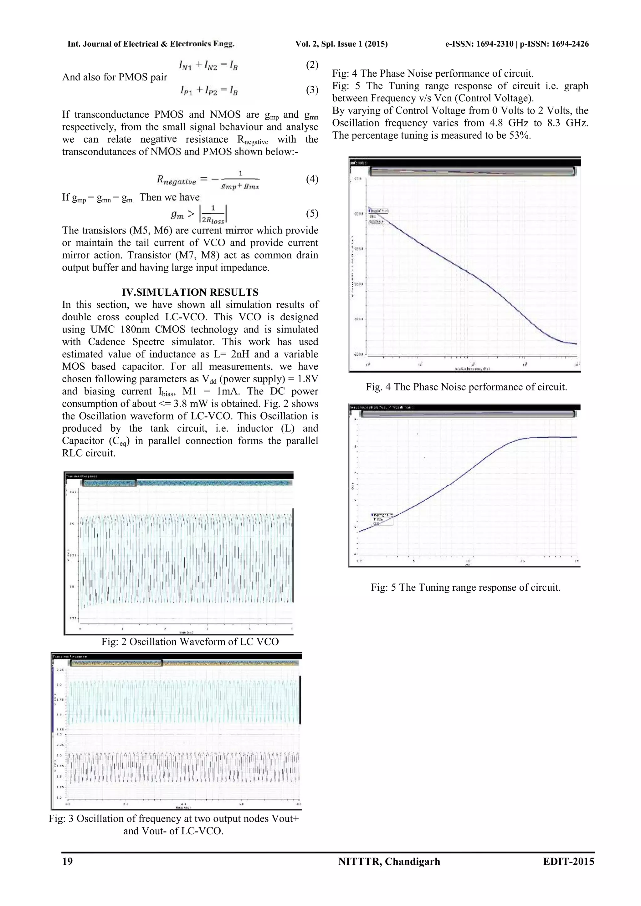
The document presents the design and simulation of a low power, low phase noise CMOS LC voltage-controlled oscillator (LC-VCO) using 180nm technology. It achieves a phase noise of approximately -96 dBc/Hz at 1 MHz, a tuning range from 4.8 to 8.3 GHz (53% tuning range), and power consumption of 3.8 mW. The design incorporates cross-coupled PMOS and NMOS transistors to enhance oscillator performance, making it suitable for various RF applications.


