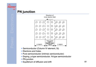
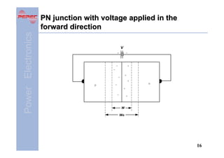
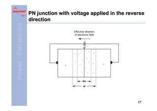
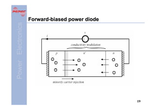
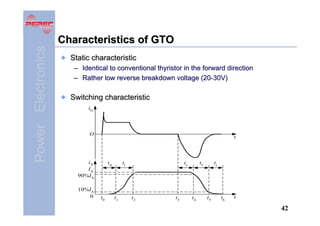
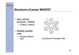
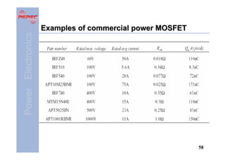
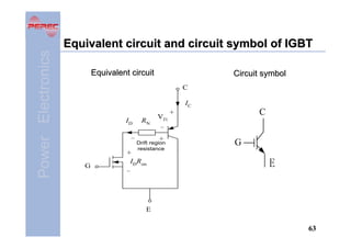
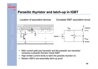
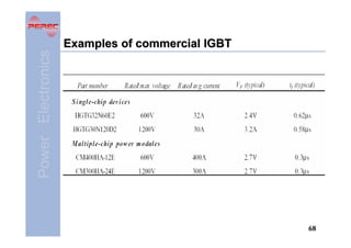
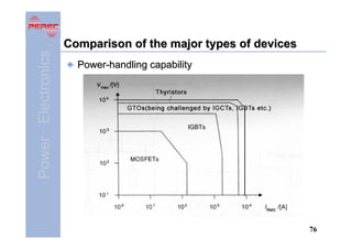
Power Electronics

Chapter 1
Power Electronic Devices
(Part I)
Power Electronics

Outline
1.1 An introductory overview of power electronic devices
1.2 Uncontrolled device — power diode
1.3 Half-controlled device — thyristor
1.4 Typical fully-controlled devices
1.5 Other new power electronic devices
1.6 Drive circuit for power electronic devices
1.7 Protection of power electronic devices
1.8 Series and parallel connections of power electronic
devices
2
Power Electronics

1.1 An introductory overview of power
electronic devices
The concept and features
Configuration of systems using power electronic devices
Classifications
Major topics

3
Power Electronics

The concept of power electronic devices
Power electronic devices:
are the electronic devices that can be directly used in the power
processing circuits to convert or control electric power.

In broad sense

Vacuum devices: Mercury arc
rectifier thyratron, etc. . seldom
in use today

power electronic devices
Semiconductor devices:
major power electronic devices

Very often: Power electronic devices = Power semiconductor devices
Major material used in power semiconductor devices
—— Silicon
4
Power Electronics

Features of power electronic devices
The electric power that power electronic device
deals with is usually much larger than that the
information electronic device does.

Usually working in switching states to reduce power
losses
On-state

Voltage across the device is 0
v=0

p=vi=0

Off-state

Current through the device is 0
i=0

p=vi=0

5
Power Electronics

Features of power electronic devices
Need to be controlled by information electronic circuits.
Very often, drive circuits are necessary to interface
between information circuits and power circuits.
Dissipated power loss usually larger than information
electronic devices — special packaging and heat sink
are necessary.

6
Power Electronics

Power losses on power semiconductor
devices
v
t

i
t

p
O n -s ta te
( c o n d u c t io n s t a t e )

tu r n in g o ff

O ff-s ta te
( b lo c k in g s t a t e )

t u r n in g
-o n

t

Total power loss on
= conduction loss + turn-off loss + off-state loss + turn-on loss
power semiconductor
(on-state loss)
Switching loss

7
Power electronic
system:

Electric isolation:
optical, magnetic

Control circuit (in a broad sense)
Control circuit

Power Electronics

Configuration of systems using power
electronic devices

detection
circuit

drive
circuit

Power circuit
(power stage,
main circuit)

Protection circuit is also very often used in power electronic
system especially for the expensive power semiconductors.
8
Power Electronics

Terminals of a power electronic device
A power electronic
device usually has
a third terminal —
—control terminal
to control the
states of the device.

C

A power electronic device
must have at least two
terminals to allow power
circuit current flow through.

G

Drive
Circuit

E

Control signal from drive circuit must be connected between the
control terminal and a fixed power circuit terminal (therefore
called common terminal ).
9
Power Electronics

A classification of power electronic devices
Uncontrolled device: diode
(Uncontrollable device)
has only two terminals and can not be controlled by control signal.
The on and off states of the device are determined by the power
circuit.

Half-controlled device: thyristor
(Half-controllable device)
is turned-on by a control signal and turned-off by the power circuit

Fully-controlled device: Power MOSFET, IGBT,GTO, IGCT
(Fully-controllable device)
The on and off states of the device are controlled by control signals.

10
Power Electronics

Other classifications
Current-driven (current-controlled) devices
power electronic devices
Voltage-driven (voltage-controlled) devices
(Field-controlled devices)
Pulse-triggered devices
power electronic devices
Level-sensitive (level-triggered) devices
Unipolar devices (Majority carrier devices)
power electronic devices

Bipolar devices (Minority carrier devices)
Composite devices

11
Power Electronics

Major topics for each device
Appearance, structure, and symbol
Physics of operation
Static characteristics

Characteristics
Switching characteristics

Specification
Special issues
Devices of the same family

12
Power Electronics

Passive components in power electronic
circuit
Transformer, inductor, capacitor and resistor:
these are passive components in a power electronic
circuit since they can not be controlled by control signal and
their characteristics are usually constant and linear.
The requirements for these passive components by power
electronic circuits could be very different from those by
ordinary circuits.

13
Power Electronics

1.2 Uncontrolled device Power diode
Appearance

Structure
Anode

Symbol
Cathode

Anode

A

K

Cathode

14
Power Electronics

PN junction
Direction of
inner electric field

- - 。 。 。

-

+

+ + +
· · ·

- - 。 。 。

-

+

- - 。 。 。

-

+

+ + +
· · ·
+ + +
· · ·

- - 。 。 。

-

+

- - 。 。 。

-

+

p region

Space charge
region
(depletion region,
potential barrier
region)

+ + +
· · ·
+ + +
· · ·
n region

Semiconductor (Column IV element, Si)
Electrons and holes.
Pure semiconductor (intrinsic semiconductor)
Doping, p-type semiconductor. N-type semiconductor
PN junction
Equilibrium of diffusion and drift

15
V
-

+

Power Electronics

PN junction with voltage applied in the
forward direction

-

+

+

-

+
p

-

n

+
-

+

W
Wo

16
Power Electronics

PN junction with voltage applied in the reverse
direction
Effective direction
of electronic field

-

+

-

+

+

-

p

+

V

+
-

+

n

+
-

-

+

+

Wo
W

17
Power Electronics

Construction of a practical power diode
Anode

i
+
p+
V

-

19

Na =10 cm

10 μm

-3

n - epi

Nd =10 cm

n+ substrate

Nd =10 cm

14

-3

Breakdown
voltage dependent

19

-3

250μm

Cathode

Features different from low-power (information electronic) diodes
– Larger size
– Vertically oriented structure
– n- drift region (p-i-n diode)
– Conductivity modulation
18
Power Electronics

Forward-biased power diode

19
Power Electronics

Reverse-biased power diode

Breakdown
– Avalanche breakdown
– Thermal breakdown
20
Power Electronics

Junction capacitor
The positive and negative charge in the depletion region is
variable with the changing of external voltage.
—–Junction capacitor CJ .
Potential barrier capacitor CB

Junction capacitor CJ
Diffusion capacitor CD

Junction capacitor influences the switching characteristics of
power diode.

21
Power Electronics

Static characteristics of power diode
I
IF

O UTO

UF

U

The I-V characteristic of power diode
22
Power Electronics

Switching (dynamic) characteristics of power
diode
Turn-off transient
IF

diF
dt

trr
td

UF
t F t0

tf
t1

t2

UR

t

diR
dt
IRP

URP

Reverse-recovery process:
Reverse-recovery time, reverse-recovery charge,
reverse-recovery peak current.
23
Power Electronics

Switching (dynamic) characteristics of power
diode
Turn-on transient
u
i
UFP

2V
0

iF

uF
tfr

t

Forward recovery process:
forward-recovery time
24
Power Electronics

Specifications of power diode
Average rectified forward current IF(AV)
Forward voltage UF
Peak repetitive reverse voltage URRM
Maximum junction temperature TJM
Reverse-recovery time trr

25
Power Electronics

Types of power diodes
General purpose diode (rectifier diode):
standard recovery

Fast recovery diode
Reverse recovery time and charge specified. trr is usually
less than 1μs, for many less than 100 ns —— ultra-fast
recovery diode.

Schottky diode (Schottky barrier diode-SBD)
– A majority carrier device
– Essentially no recovered charge, and lower forward voltage.
– Restricted to low voltage (less than 200V)

26
Power Electronics

Examples of commercial power diodes

27
Power Electronics

History and applications of power diode
Applied in industries starting 1950s
Still in-use today. Usually working with controlled
devices as necessary components
In many circumstances fast recovery diodes or
schottky diodes have to be used instead of general
purpose diodes.

28
Power Electronics

1.3 Half-controlled device—Thyristor
History
Another name: SCR—silicon controlled rectifier
Thyristor Opened the power electronics era
–
–
–
–

1956, invention, Bell Laboratories
1957, development of the 1st product, GE
1958, 1st commercialized product, GE
Thyristor replaced vacuum devices in almost every power
processing area.

Still in use in high power situation. Thyristor till has the
highest power-handling capability.

29
Power Electronics

Appearance and symbol of thyristor
Appearance

Symbol

Cathode

K

Gate
Anode

G

A

30
Power Electronics

Structure and equivalent circuit of thyristor
• Structure

• Equivalent circuit

31
Power Electronics

Physics of thyristor operation
Equivalent circuit: A pnp
transistor and an npn transistor
interconnected together
Positive feedback
Trigger
Can not be turned off by control
signal
Half-controllable

32
Power Electronics

Quantitative description of thyristor operation
Ic1=α1 IA + ICBO1

(1-1)

Ic2=α2 IK + ICBO2

(1-2)

IK=IA+IG

(1-3)

IA=Ic1+Ic2

(1-4)

α2IG + ICBO1+ ICBO2
IA =
1− (α1 +α2 )

(1-5)

When IG=0, α1+α2 is small.
When IG>0, α1+α2 will approach 1, IA will be very large.

33
Power Electronics

Other methods to trigger thyristor on
High voltage across anode and cathode—
avalanche breakdown
High rising rate of anode voltagte — du/dt too high
High junction temperature
Light activation

34
Power Electronics

Static characteristics of thyristor
IA

forward
conducting

increasing IG

I

U RSM U RRM
reverse
blocking

avalanche
breakdown

I G2

IG = 0

I G1

H

O

forward
blocking

U DRM

U bo

U DSM

U Ak

Blocking when reverse
biased, no matter if there
is gate current applied
Conducting only when
forward biased and there
is triggering current
applied to the gate
Once triggered on, will be
latched on conducting
even when the gate
current is no longer
applied
Turning off: decreasing
current to be near zero
with the effect of external
power circuit
Gate I-V characteristics
35
Power Electronics

Switching characteristics of thyristor
iA
100%
90%

10%
0 td
uAK

Turn-on transient
–
–
–
tr

Delay time td
Rise time tr
Turn-on time tgt

t

Turn-off transient
IRM

t

O

trr

– Reverse recovery
time trr
– Forward recovery
time tgr
– Turn-off time tq

URRM t
gr

36
Power Electronics

Specifications of thyristor
Peak repetitive forward blocking voltage UDRM
Peak repetitive reverse blocking voltage URRM
Peak on-state voltage UTM
Average on-state current IT(AV)
Holding current IH
Latching up current IL
Peak forward surge current ITSM
du/dt
di/dt

37
Power Electronics

The family of thyristors
Fast switching thyristor—FST
Triode AC switch—TRIAC
(Bi-directional triode thyristor)

I

IG=0

T1

O

G

U

T2

Reverse-conducting thyristor
—RCT
K

Light-triggered (activited) thyristor
—LTT
A

K

G

G

G
A

K
A

38
Power Electronics

1.4 Typical fully-controlled devices
1.4.1 Gate-turn-off thyristor —GTO
1.4.2 Giant transistor —GTR
1.4.3 Power metal-oxide-semiconductor field effect
transistor — Power MOSFET
1.4.4 Insulated-gate bipolar transistor —IGBT

Features
– IC fabrication technology, fully-controllable, high frequency

Applications
– Begin to be used in large amount in 1980s
– GTR is obsolete and GTO is also seldom used today.
– IGBT and power MOSFET are the two major power
semiconductor devices nowadays.
39
Power Electronics

1.4.1 Gate-turn-off thyristor—GTO
Structure

Symbol
A
G

K

N2

K

G

P2
N1

G

N2

G

P1
A
a)

K

b)

Major difference from conventional thyristor:
The gate and cathode structures are highly interdigitated, with
various types of geometric forms being used to layout the
gates and cathodes.
40
Power Electronics

Physics of GTO operation
The basic operation of GTO is the
same as that of the conventional
thyristor.

A
IA

PNP

V1
G IG
S
EG

Ic2
Ic1
NPN

R

V2
IK
K

EA

The principal differences lie in the
modifications in the structure to
achieve gate turn-off capability.
– Large α2
– α1+α2 is just a little larger than
the critical value 1.
– Short distance from gate to
cathode makes it possible to
drive current out of gate.

41
Power Electronics

Characteristics of GTO
Static characteristic
– Identical to conventional thyristor in the forward direction
– Rather low reverse breakdown voltage (20-30V)

Switching characteristic
iG

O

t

iA
IA
90%IA
10%IA
0

td

t0

tr

t1

ts

t2

t3

tf

t4

tt

t5

t6

t

42
Power Electronics

Specifications of GTO
Most GTO specifications have the same meanings
as those of conventional thyristor.
Specifications different from thyristor’s
–
–
–
–

Maximum controllable anode current IATO
Current turn-off gain βoff
Turn-on time ton
Turn-off time toff

43
Power Electronics

1.4.2 Giant Transistor—GTR
GTR is actually the bipolar junction transistor that can handle
high voltage and large current.
So GTR is also called power BJT, or just BJT.

Basic structure

Symbol
c

b

e

44
Power Electronics

Structures of GTR different from its
information-processing counterpart
Multiple-emitter structure

Darlington configuration

45
Power Electronics

Physics of GTR operation
Same as information BJT device
i c= β ib

holes
ib
Ec
Eb

electrons
i e =(1+ β )ib

46
region

I

Saturatio
n

Power Electronics

Static characteristics of GTR

Amplifying (active) region

ib3
ib2
ib1

ib1<ib2<ib3

cut-off region

O

Uce
47
Power Electronics

Switching characteristics of GTR
ib

Ib

90%Ib1

1

Turn-on transient
– Turn-on delay time td
– Rise time tr
– Turn-on time ton

10%Ib1
0

t
Ib

Turn-off transient

2

toff

ton
ic

td tr

ts

Ics

– Storage time ts
– Falling time tf

tf

90%Ics
10%Ics
0

– Turn-off time toff

t0 t1

t2

t3

t4

t5

t
48
Power Electronics

Second breakdown of GTR

49
Power Electronics

Safe operating area (SOA) of GTR
Ic
P SB

IcM

SO A

O

P cM

U ceM

U ce
50
Power Electronics

1.4.3 Power metal-oxide-semiconductor field
effect transistor—Power MOSFET
A classification
Field Effect
Transistor
(FET)

Metal-onside-semiconductor FET (MOSFET)
n channel
p channel
Junction FET (JFET)

Power MOSFET

Static induction transistor (SIT)

Basic structure

Symbol
D

D

G

G
S
N channel

S
P channel

51
Power Electronics

Structures of power MOSFET

Also vertical
structure—VMOS
– VVMOS, VDMOS

Multiple parallel
cells
– Polygon-shaped
cells

A structure of hexagon cells

52
Power Electronics

Physics of MOSFET operation
Off-state
p-n- junction is
reverse-biased
off-state voltage
appears across
n- region

53
Power Electronics

Physics of MOSFET operation
On-state
p-n- junction is slightly
reverse biased
positive gate voltage
induces conducting
channel
drain current flows
through n- region and
conducting channel
on resistance = total
resistances of n- region,
conducting
channel,source and drain
contacts, etc.

54
Power Electronics

Static characteristics of power MOSFET

55
Power Electronics

Switching characteristics of power MOSFET
+UE

up

RL

O

iD
Rs
up

RG uGS R
F

iD

t

uGS
uGSP
uT
O
iD

t

Ot
d(on)

Turn-on transient
– Turn-on delay time td(on)
– Rise time tr

tr

td(off)

tf

t

Turn-off transient
– Turn-off delay time td(off)
– Falling time tf

56
Power Electronics

Specifications of power MOSFET
Drain-source breakdown voltage UDS
Continuous drain current ID
Peak pulsed drain current IDM
On (On-state) resistance RDS(on)
Inter-terminal capacitances
– Short circuit input capacitance Ciss= CGS+ CGD
– Reverse transfer capacitance Crss= CGD
– Short circuit output capacitance Coss= CDS+ CGD

SOA of power MOSFET
– No second breakdown

57
Power Electronics

Examples of commercial power MOSFET

58
Power Electronics

Features and applications of power MOSFET
Voltage-driven device, simple drive circuit
Majority-carrier device, fast switching speed, high
operating frequency (could be hundreds of kHz)
Majority-carrier device, better thermal stability
On-resistance increases rapidly with rated blocking
voltage
– Usually used at voltages less than 500V and power less
than 10kW
– 1000V devices are available, but are useful only at low
power levels(100W)

Part number is selected on the basis of onresistance rather than current rating
59
Power Electronics

The body diode of power MOSFET
The body diode

Equivalent circuit

60
Power Electronics

1.4.4 Insulated-gate bipolar transistor
—IGBT
Combination of MOSFET and GTR
GTR:

low conduction losses (especially at larger blocking voltages),
longer switching times, current-driven

MOSFET:

IGBT

faster switching speed, easy to drive (voltage-driven),
larger conduction losses (especially for higher blocking voltages)

Features
• On-state losses are much smaller than those of a power
MOSFET, and are comparable with those of a GTR
• Easy to drive —similar to power MOSFET
• Faster than GTR, but slower than power MOSFET
Application
• The device of choice in 500-1700V applications, at power
levels of several kW to several MW
61
Power Electronics

Structure and operation principle of IGBT
Basic structure
Emitter
E

Gate
G

N + N+
N+ N +
P
P
J3 J
N
2
N+
J1
P+
C
a)

Collector

Drift region
Buffer layer
Injecting layer

Also multiple cell structure
Basic structure similar to
power MOSFET, except
extra p region
On-state: minority carriers
are injected into drift region,
leading to conductivity
modulation
compared with power
MOSFET: slower switching
times, lower on-resistance,
useful at higher voltages
(up to 1700V)

62
Power Electronics

Equivalent circuit and circuit symbol of IGBT
Equivalent circuit

Circuit symbol
C
IC

ID
-

G

RN

VJ1
+

Drift region
resistance

+
IDRon
-

C

+

G

E

E

63
Power Electronics

Static characteristics of IGBT
IC

Active region

Saturation region
(On region)
UGE

URM

Reverse
blocking region
O

UGE(th)
Cut-off (forward
blocking) region

UFM UCE

64
Power Electronics

Switching characteristics of IGBT
UGE

UGEM

IGBT turn-on is
similar to power
MOSFET turn-on

90%UGEM
10%UGEM
0
IC
90% ICM

t

ICM
td(on)

tr

td(off)
tfi1

10% ICM
0
UCE

tf
tfi2
current tail

ton

toff

UCEM

tfv1

t

tfv2

The major
difference between
IGBT turn-off and
power MOSFET
turn-off:
– There is current
tailing in the IGBT
turn-off due to the
stored charge in
the drift region.

UCE(on)
O

t

65
Power Electronics

Parasitic thyristor and latch-up in IGBT
Location of equivalent devices

Complete IGBT equivalent circuit

Main current path pnp transistor and the parasitic npn transistor
compose a parasitic thyristor inside IGBT.
High emitter current tends to latch the parasitic thyristor on.
Modern IGBTs are essentially latch-up proof
66
Power Electronics

Specifications of IGBT
Collector-emitter breakdown voltage UCES
Continuous collector current IC
Peak pulsed collector current ICM
Maximum power dissipation PCM
Other issues:
SOA of IGBT
– The IGBT has a rectangular SOA with similar shape to the
power MOSFET.

Usually fabricated with an anti-parallel fast diode

67
Power Electronics

Examples of commercial IGBT

68
Power Electronics

1.5 Other new power electronic devices
Static induction transistor —SIT
Static induction thyristor —SITH
MOS controlled thyristor — MCT
Integrated gate-commutated thyristor —IGCT
Power integrated circuit and power module

69
Power Electronics

Static induction transistor—SIT
Another name: power junction field effect
transistor—power JFET
Features
–
–
–
–
–

Major-carrier device
Fast switching, comparable to power MOSFET
Higher power-handling capability than power MOSFET
Higher conduction losses than power MOSFET
Normally-on device, not convenient (could be made
normally-off, but with even higher on-state losses)

70
Power Electronics

Static induction thyristor—SITH
other names
– Field controlled thyristor—FCT
– Field controlled diode

Features
– Minority-carrier device, a JFET structure with an additional
injecting layer
– Power-handling capability similar to GTO
– Faster switching speeds than GTO
– Normally-on device, not convenient (could be made
normally-off, but with even higher on-state losses)

71
Power Electronics

MOS controlled thyristor—MCT
Essentially a GTO with integrated MOS-driven
gates controlling both turn-on and turn-off that
potentially will significantly simply the design of
circuits using GTO.
The difficulty is how to design a MCT that can be
turned on and turned off equally well.
Once believed as the most promising device, but
still not commercialized in a large scale. The future
remains uncertain.

72
Power Electronics

Integrated gate-commutated thyristor — IGCT
The newest member of the power semiconductor
family, introduced in 1997 by ABB
Actually the close integration of GTO and the gate
drive circuit with multiple MOSFETs in parallel
providing the gate currents
Short name: GCT
Conduction drop, gate driver loss, and switching
speed are superior to GTO
Competing with IGBT and other new devices to
replace GTO

73
Power Electronics

Power integrated circuit and power module
Monolithic integration:
power integrated circuit

Integration of
power electronic
devices

High voltage integrated circuit (HVIC)
Smart power integrated circuit(Smart
power IC, SPIC, Smart switch)

Ordinary power module:just power
devices packaged together

Packaging integration:
power module

Intelligent power module (IPM):
power devices, drive circuit, protection
circuit
Integrated power electronics
Module(IPEM): power devices, drive
circuit, protection circuit, control circuit

Two major challenges
– Electrical isolation of high-voltage components from lowvoltage components
– Thermal management—power devices usually at higher
temperatures than low-voltage devices
74
Power Electronics

Review of device classifications
power electronic
devices

Current-driven (current-controlled) devices:
thyristor, GTO, GTR
Voltage-driven (voltage-controlled) devices
(Field-controlled devices):power MOSFET,
IGBT, SIT, SITH, MCT, IGCT
Pulse-triggered devices: thyristor, GTO

power electronic
devices

Level-sensitive (Level-triggered) devices:
GTR,power MOSFET, IGBT, SIT, SITH,
MCT, IGCT
Uni-polar devices (Majority carrier devices):
SBD, power MOSFET, SIT

power electronic
devices

Bipolar devices (Minority carrier devices):
ordinary power diode, thyristor, GTO, GTR,
IGCT, IGBT, SITH, MCT
Composite devices: IGBT, SITH, MCT
75
Power Electronics

Comparison of the major types of devices
Power-handling capability

76
Power Electronics

Comparison of the major types of devices
Maximum allowed current density as a function of
the switching frequency

77

POWER ELECTRONIC DEVICES

  • 1.
    Power Electronics Chapter 1 PowerElectronic Devices (Part I)
  • 2.
    Power Electronics Outline 1.1 Anintroductory overview of power electronic devices 1.2 Uncontrolled device — power diode 1.3 Half-controlled device — thyristor 1.4 Typical fully-controlled devices 1.5 Other new power electronic devices 1.6 Drive circuit for power electronic devices 1.7 Protection of power electronic devices 1.8 Series and parallel connections of power electronic devices 2
  • 3.
    Power Electronics 1.1 Anintroductory overview of power electronic devices The concept and features Configuration of systems using power electronic devices Classifications Major topics 3
  • 4.
    Power Electronics The conceptof power electronic devices Power electronic devices: are the electronic devices that can be directly used in the power processing circuits to convert or control electric power. In broad sense Vacuum devices: Mercury arc rectifier thyratron, etc. . seldom in use today power electronic devices Semiconductor devices: major power electronic devices Very often: Power electronic devices = Power semiconductor devices Major material used in power semiconductor devices —— Silicon 4
  • 5.
    Power Electronics Features ofpower electronic devices The electric power that power electronic device deals with is usually much larger than that the information electronic device does. Usually working in switching states to reduce power losses On-state Voltage across the device is 0 v=0 p=vi=0 Off-state Current through the device is 0 i=0 p=vi=0 5
  • 6.
    Power Electronics Features ofpower electronic devices Need to be controlled by information electronic circuits. Very often, drive circuits are necessary to interface between information circuits and power circuits. Dissipated power loss usually larger than information electronic devices — special packaging and heat sink are necessary. 6
  • 7.
    Power Electronics Power losseson power semiconductor devices v t i t p O n -s ta te ( c o n d u c t io n s t a t e ) tu r n in g o ff O ff-s ta te ( b lo c k in g s t a t e ) t u r n in g -o n t Total power loss on = conduction loss + turn-off loss + off-state loss + turn-on loss power semiconductor (on-state loss) Switching loss 7
  • 8.
    Power electronic system: Electric isolation: optical,magnetic Control circuit (in a broad sense) Control circuit Power Electronics Configuration of systems using power electronic devices detection circuit drive circuit Power circuit (power stage, main circuit) Protection circuit is also very often used in power electronic system especially for the expensive power semiconductors. 8
  • 9.
    Power Electronics Terminals ofa power electronic device A power electronic device usually has a third terminal — —control terminal to control the states of the device. C A power electronic device must have at least two terminals to allow power circuit current flow through. G Drive Circuit E Control signal from drive circuit must be connected between the control terminal and a fixed power circuit terminal (therefore called common terminal ). 9
  • 10.
    Power Electronics A classificationof power electronic devices Uncontrolled device: diode (Uncontrollable device) has only two terminals and can not be controlled by control signal. The on and off states of the device are determined by the power circuit. Half-controlled device: thyristor (Half-controllable device) is turned-on by a control signal and turned-off by the power circuit Fully-controlled device: Power MOSFET, IGBT,GTO, IGCT (Fully-controllable device) The on and off states of the device are controlled by control signals. 10
  • 11.
    Power Electronics Other classifications Current-driven(current-controlled) devices power electronic devices Voltage-driven (voltage-controlled) devices (Field-controlled devices) Pulse-triggered devices power electronic devices Level-sensitive (level-triggered) devices Unipolar devices (Majority carrier devices) power electronic devices Bipolar devices (Minority carrier devices) Composite devices 11
  • 12.
    Power Electronics Major topicsfor each device Appearance, structure, and symbol Physics of operation Static characteristics Characteristics Switching characteristics Specification Special issues Devices of the same family 12
  • 13.
    Power Electronics Passive componentsin power electronic circuit Transformer, inductor, capacitor and resistor: these are passive components in a power electronic circuit since they can not be controlled by control signal and their characteristics are usually constant and linear. The requirements for these passive components by power electronic circuits could be very different from those by ordinary circuits. 13
  • 14.
    Power Electronics 1.2 Uncontrolleddevice Power diode Appearance Structure Anode Symbol Cathode Anode A K Cathode 14
  • 15.
    Power Electronics PN junction Directionof inner electric field - - 。 。 。 - + + + + · · · - - 。 。 。 - + - - 。 。 。 - + + + + · · · + + + · · · - - 。 。 。 - + - - 。 。 。 - + p region Space charge region (depletion region, potential barrier region) + + + · · · + + + · · · n region Semiconductor (Column IV element, Si) Electrons and holes. Pure semiconductor (intrinsic semiconductor) Doping, p-type semiconductor. N-type semiconductor PN junction Equilibrium of diffusion and drift 15
  • 16.
    V - + Power Electronics PN junctionwith voltage applied in the forward direction - + + - + p - n + - + W Wo 16
  • 17.
    Power Electronics PN junctionwith voltage applied in the reverse direction Effective direction of electronic field - + - + + - p + V + - + n + - - + + Wo W 17
  • 18.
    Power Electronics Construction ofa practical power diode Anode i + p+ V - 19 Na =10 cm 10 μm -3 n - epi Nd =10 cm n+ substrate Nd =10 cm 14 -3 Breakdown voltage dependent 19 -3 250μm Cathode Features different from low-power (information electronic) diodes – Larger size – Vertically oriented structure – n- drift region (p-i-n diode) – Conductivity modulation 18
  • 19.
  • 20.
    Power Electronics Reverse-biased powerdiode Breakdown – Avalanche breakdown – Thermal breakdown 20
  • 21.
    Power Electronics Junction capacitor Thepositive and negative charge in the depletion region is variable with the changing of external voltage. —–Junction capacitor CJ . Potential barrier capacitor CB Junction capacitor CJ Diffusion capacitor CD Junction capacitor influences the switching characteristics of power diode. 21
  • 22.
    Power Electronics Static characteristicsof power diode I IF O UTO UF U The I-V characteristic of power diode 22
  • 23.
    Power Electronics Switching (dynamic)characteristics of power diode Turn-off transient IF diF dt trr td UF t F t0 tf t1 t2 UR t diR dt IRP URP Reverse-recovery process: Reverse-recovery time, reverse-recovery charge, reverse-recovery peak current. 23
  • 24.
    Power Electronics Switching (dynamic)characteristics of power diode Turn-on transient u i UFP 2V 0 iF uF tfr t Forward recovery process: forward-recovery time 24
  • 25.
    Power Electronics Specifications ofpower diode Average rectified forward current IF(AV) Forward voltage UF Peak repetitive reverse voltage URRM Maximum junction temperature TJM Reverse-recovery time trr 25
  • 26.
    Power Electronics Types ofpower diodes General purpose diode (rectifier diode): standard recovery Fast recovery diode Reverse recovery time and charge specified. trr is usually less than 1μs, for many less than 100 ns —— ultra-fast recovery diode. Schottky diode (Schottky barrier diode-SBD) – A majority carrier device – Essentially no recovered charge, and lower forward voltage. – Restricted to low voltage (less than 200V) 26
  • 27.
    Power Electronics Examples ofcommercial power diodes 27
  • 28.
    Power Electronics History andapplications of power diode Applied in industries starting 1950s Still in-use today. Usually working with controlled devices as necessary components In many circumstances fast recovery diodes or schottky diodes have to be used instead of general purpose diodes. 28
  • 29.
    Power Electronics 1.3 Half-controlleddevice—Thyristor History Another name: SCR—silicon controlled rectifier Thyristor Opened the power electronics era – – – – 1956, invention, Bell Laboratories 1957, development of the 1st product, GE 1958, 1st commercialized product, GE Thyristor replaced vacuum devices in almost every power processing area. Still in use in high power situation. Thyristor till has the highest power-handling capability. 29
  • 30.
    Power Electronics Appearance andsymbol of thyristor Appearance Symbol Cathode K Gate Anode G A 30
  • 31.
    Power Electronics Structure andequivalent circuit of thyristor • Structure • Equivalent circuit 31
  • 32.
    Power Electronics Physics ofthyristor operation Equivalent circuit: A pnp transistor and an npn transistor interconnected together Positive feedback Trigger Can not be turned off by control signal Half-controllable 32
  • 33.
    Power Electronics Quantitative descriptionof thyristor operation Ic1=α1 IA + ICBO1 (1-1) Ic2=α2 IK + ICBO2 (1-2) IK=IA+IG (1-3) IA=Ic1+Ic2 (1-4) α2IG + ICBO1+ ICBO2 IA = 1− (α1 +α2 ) (1-5) When IG=0, α1+α2 is small. When IG>0, α1+α2 will approach 1, IA will be very large. 33
  • 34.
    Power Electronics Other methodsto trigger thyristor on High voltage across anode and cathode— avalanche breakdown High rising rate of anode voltagte — du/dt too high High junction temperature Light activation 34
  • 35.
    Power Electronics Static characteristicsof thyristor IA forward conducting increasing IG I U RSM U RRM reverse blocking avalanche breakdown I G2 IG = 0 I G1 H O forward blocking U DRM U bo U DSM U Ak Blocking when reverse biased, no matter if there is gate current applied Conducting only when forward biased and there is triggering current applied to the gate Once triggered on, will be latched on conducting even when the gate current is no longer applied Turning off: decreasing current to be near zero with the effect of external power circuit Gate I-V characteristics 35
  • 36.
    Power Electronics Switching characteristicsof thyristor iA 100% 90% 10% 0 td uAK Turn-on transient – – – tr Delay time td Rise time tr Turn-on time tgt t Turn-off transient IRM t O trr – Reverse recovery time trr – Forward recovery time tgr – Turn-off time tq URRM t gr 36
  • 37.
    Power Electronics Specifications ofthyristor Peak repetitive forward blocking voltage UDRM Peak repetitive reverse blocking voltage URRM Peak on-state voltage UTM Average on-state current IT(AV) Holding current IH Latching up current IL Peak forward surge current ITSM du/dt di/dt 37
  • 38.
    Power Electronics The familyof thyristors Fast switching thyristor—FST Triode AC switch—TRIAC (Bi-directional triode thyristor) I IG=0 T1 O G U T2 Reverse-conducting thyristor —RCT K Light-triggered (activited) thyristor —LTT A K G G G A K A 38
  • 39.
    Power Electronics 1.4 Typicalfully-controlled devices 1.4.1 Gate-turn-off thyristor —GTO 1.4.2 Giant transistor —GTR 1.4.3 Power metal-oxide-semiconductor field effect transistor — Power MOSFET 1.4.4 Insulated-gate bipolar transistor —IGBT Features – IC fabrication technology, fully-controllable, high frequency Applications – Begin to be used in large amount in 1980s – GTR is obsolete and GTO is also seldom used today. – IGBT and power MOSFET are the two major power semiconductor devices nowadays. 39
  • 40.
    Power Electronics 1.4.1 Gate-turn-offthyristor—GTO Structure Symbol A G K N2 K G P2 N1 G N2 G P1 A a) K b) Major difference from conventional thyristor: The gate and cathode structures are highly interdigitated, with various types of geometric forms being used to layout the gates and cathodes. 40
  • 41.
    Power Electronics Physics ofGTO operation The basic operation of GTO is the same as that of the conventional thyristor. A IA PNP V1 G IG S EG Ic2 Ic1 NPN R V2 IK K EA The principal differences lie in the modifications in the structure to achieve gate turn-off capability. – Large α2 – α1+α2 is just a little larger than the critical value 1. – Short distance from gate to cathode makes it possible to drive current out of gate. 41
  • 42.
    Power Electronics Characteristics ofGTO Static characteristic – Identical to conventional thyristor in the forward direction – Rather low reverse breakdown voltage (20-30V) Switching characteristic iG O t iA IA 90%IA 10%IA 0 td t0 tr t1 ts t2 t3 tf t4 tt t5 t6 t 42
  • 43.
    Power Electronics Specifications ofGTO Most GTO specifications have the same meanings as those of conventional thyristor. Specifications different from thyristor’s – – – – Maximum controllable anode current IATO Current turn-off gain βoff Turn-on time ton Turn-off time toff 43
  • 44.
    Power Electronics 1.4.2 GiantTransistor—GTR GTR is actually the bipolar junction transistor that can handle high voltage and large current. So GTR is also called power BJT, or just BJT. Basic structure Symbol c b e 44
  • 45.
    Power Electronics Structures ofGTR different from its information-processing counterpart Multiple-emitter structure Darlington configuration 45
  • 46.
    Power Electronics Physics ofGTR operation Same as information BJT device i c= β ib holes ib Ec Eb electrons i e =(1+ β )ib 46
  • 47.
    region I Saturatio n Power Electronics Static characteristicsof GTR Amplifying (active) region ib3 ib2 ib1 ib1<ib2<ib3 cut-off region O Uce 47
  • 48.
    Power Electronics Switching characteristicsof GTR ib Ib 90%Ib1 1 Turn-on transient – Turn-on delay time td – Rise time tr – Turn-on time ton 10%Ib1 0 t Ib Turn-off transient 2 toff ton ic td tr ts Ics – Storage time ts – Falling time tf tf 90%Ics 10%Ics 0 – Turn-off time toff t0 t1 t2 t3 t4 t5 t 48
  • 49.
  • 50.
    Power Electronics Safe operatingarea (SOA) of GTR Ic P SB IcM SO A O P cM U ceM U ce 50
  • 51.
    Power Electronics 1.4.3 Powermetal-oxide-semiconductor field effect transistor—Power MOSFET A classification Field Effect Transistor (FET) Metal-onside-semiconductor FET (MOSFET) n channel p channel Junction FET (JFET) Power MOSFET Static induction transistor (SIT) Basic structure Symbol D D G G S N channel S P channel 51
  • 52.
    Power Electronics Structures ofpower MOSFET Also vertical structure—VMOS – VVMOS, VDMOS Multiple parallel cells – Polygon-shaped cells A structure of hexagon cells 52
  • 53.
    Power Electronics Physics ofMOSFET operation Off-state p-n- junction is reverse-biased off-state voltage appears across n- region 53
  • 54.
    Power Electronics Physics ofMOSFET operation On-state p-n- junction is slightly reverse biased positive gate voltage induces conducting channel drain current flows through n- region and conducting channel on resistance = total resistances of n- region, conducting channel,source and drain contacts, etc. 54
  • 55.
  • 56.
    Power Electronics Switching characteristicsof power MOSFET +UE up RL O iD Rs up RG uGS R F iD t uGS uGSP uT O iD t Ot d(on) Turn-on transient – Turn-on delay time td(on) – Rise time tr tr td(off) tf t Turn-off transient – Turn-off delay time td(off) – Falling time tf 56
  • 57.
    Power Electronics Specifications ofpower MOSFET Drain-source breakdown voltage UDS Continuous drain current ID Peak pulsed drain current IDM On (On-state) resistance RDS(on) Inter-terminal capacitances – Short circuit input capacitance Ciss= CGS+ CGD – Reverse transfer capacitance Crss= CGD – Short circuit output capacitance Coss= CDS+ CGD SOA of power MOSFET – No second breakdown 57
  • 58.
    Power Electronics Examples ofcommercial power MOSFET 58
  • 59.
    Power Electronics Features andapplications of power MOSFET Voltage-driven device, simple drive circuit Majority-carrier device, fast switching speed, high operating frequency (could be hundreds of kHz) Majority-carrier device, better thermal stability On-resistance increases rapidly with rated blocking voltage – Usually used at voltages less than 500V and power less than 10kW – 1000V devices are available, but are useful only at low power levels(100W) Part number is selected on the basis of onresistance rather than current rating 59
  • 60.
    Power Electronics The bodydiode of power MOSFET The body diode Equivalent circuit 60
  • 61.
    Power Electronics 1.4.4 Insulated-gatebipolar transistor —IGBT Combination of MOSFET and GTR GTR: low conduction losses (especially at larger blocking voltages), longer switching times, current-driven MOSFET: IGBT faster switching speed, easy to drive (voltage-driven), larger conduction losses (especially for higher blocking voltages) Features • On-state losses are much smaller than those of a power MOSFET, and are comparable with those of a GTR • Easy to drive —similar to power MOSFET • Faster than GTR, but slower than power MOSFET Application • The device of choice in 500-1700V applications, at power levels of several kW to several MW 61
  • 62.
    Power Electronics Structure andoperation principle of IGBT Basic structure Emitter E Gate G N + N+ N+ N + P P J3 J N 2 N+ J1 P+ C a) Collector Drift region Buffer layer Injecting layer Also multiple cell structure Basic structure similar to power MOSFET, except extra p region On-state: minority carriers are injected into drift region, leading to conductivity modulation compared with power MOSFET: slower switching times, lower on-resistance, useful at higher voltages (up to 1700V) 62
  • 63.
    Power Electronics Equivalent circuitand circuit symbol of IGBT Equivalent circuit Circuit symbol C IC ID - G RN VJ1 + Drift region resistance + IDRon - C + G E E 63
  • 64.
    Power Electronics Static characteristicsof IGBT IC Active region Saturation region (On region) UGE URM Reverse blocking region O UGE(th) Cut-off (forward blocking) region UFM UCE 64
  • 65.
    Power Electronics Switching characteristicsof IGBT UGE UGEM IGBT turn-on is similar to power MOSFET turn-on 90%UGEM 10%UGEM 0 IC 90% ICM t ICM td(on) tr td(off) tfi1 10% ICM 0 UCE tf tfi2 current tail ton toff UCEM tfv1 t tfv2 The major difference between IGBT turn-off and power MOSFET turn-off: – There is current tailing in the IGBT turn-off due to the stored charge in the drift region. UCE(on) O t 65
  • 66.
    Power Electronics Parasitic thyristorand latch-up in IGBT Location of equivalent devices Complete IGBT equivalent circuit Main current path pnp transistor and the parasitic npn transistor compose a parasitic thyristor inside IGBT. High emitter current tends to latch the parasitic thyristor on. Modern IGBTs are essentially latch-up proof 66
  • 67.
    Power Electronics Specifications ofIGBT Collector-emitter breakdown voltage UCES Continuous collector current IC Peak pulsed collector current ICM Maximum power dissipation PCM Other issues: SOA of IGBT – The IGBT has a rectangular SOA with similar shape to the power MOSFET. Usually fabricated with an anti-parallel fast diode 67
  • 68.
  • 69.
    Power Electronics 1.5 Othernew power electronic devices Static induction transistor —SIT Static induction thyristor —SITH MOS controlled thyristor — MCT Integrated gate-commutated thyristor —IGCT Power integrated circuit and power module 69
  • 70.
    Power Electronics Static inductiontransistor—SIT Another name: power junction field effect transistor—power JFET Features – – – – – Major-carrier device Fast switching, comparable to power MOSFET Higher power-handling capability than power MOSFET Higher conduction losses than power MOSFET Normally-on device, not convenient (could be made normally-off, but with even higher on-state losses) 70
  • 71.
    Power Electronics Static inductionthyristor—SITH other names – Field controlled thyristor—FCT – Field controlled diode Features – Minority-carrier device, a JFET structure with an additional injecting layer – Power-handling capability similar to GTO – Faster switching speeds than GTO – Normally-on device, not convenient (could be made normally-off, but with even higher on-state losses) 71
  • 72.
    Power Electronics MOS controlledthyristor—MCT Essentially a GTO with integrated MOS-driven gates controlling both turn-on and turn-off that potentially will significantly simply the design of circuits using GTO. The difficulty is how to design a MCT that can be turned on and turned off equally well. Once believed as the most promising device, but still not commercialized in a large scale. The future remains uncertain. 72
  • 73.
    Power Electronics Integrated gate-commutatedthyristor — IGCT The newest member of the power semiconductor family, introduced in 1997 by ABB Actually the close integration of GTO and the gate drive circuit with multiple MOSFETs in parallel providing the gate currents Short name: GCT Conduction drop, gate driver loss, and switching speed are superior to GTO Competing with IGBT and other new devices to replace GTO 73
  • 74.
    Power Electronics Power integratedcircuit and power module Monolithic integration: power integrated circuit Integration of power electronic devices High voltage integrated circuit (HVIC) Smart power integrated circuit(Smart power IC, SPIC, Smart switch) Ordinary power module:just power devices packaged together Packaging integration: power module Intelligent power module (IPM): power devices, drive circuit, protection circuit Integrated power electronics Module(IPEM): power devices, drive circuit, protection circuit, control circuit Two major challenges – Electrical isolation of high-voltage components from lowvoltage components – Thermal management—power devices usually at higher temperatures than low-voltage devices 74
  • 75.
    Power Electronics Review ofdevice classifications power electronic devices Current-driven (current-controlled) devices: thyristor, GTO, GTR Voltage-driven (voltage-controlled) devices (Field-controlled devices):power MOSFET, IGBT, SIT, SITH, MCT, IGCT Pulse-triggered devices: thyristor, GTO power electronic devices Level-sensitive (Level-triggered) devices: GTR,power MOSFET, IGBT, SIT, SITH, MCT, IGCT Uni-polar devices (Majority carrier devices): SBD, power MOSFET, SIT power electronic devices Bipolar devices (Minority carrier devices): ordinary power diode, thyristor, GTO, GTR, IGCT, IGBT, SITH, MCT Composite devices: IGBT, SITH, MCT 75
  • 76.
    Power Electronics Comparison ofthe major types of devices Power-handling capability 76
  • 77.
    Power Electronics Comparison ofthe major types of devices Maximum allowed current density as a function of the switching frequency 77