Download to read offline
![Int. Journal of Electrical & Electronics Engg. Vol. 2, Spl. Issue 1 (2015) e-ISSN: 1694-2310 | p-ISSN: 1694-2426
NITTTR, Chandigarh EDIT -2015 60
Layout Design Implementation of NOR Gate
Nishali
Department of ECE, Jasdev Singh Sandhu Institute of Engineering and Technology, Punjab, India
rai.nishali@gmail.com
ABSTRACT: In this paper VLSI design have been
introduce decrease the area and power CMOS 90 nm
technology is used for designing nor gate. The power
consumption and area of nor gate compared in this paper.
The proposed design reduces the power consumption and
area. The nor gate reduces power consumption by 46%
and area by 67% .two design flow are implement, fully
automatic and semicustom .the semicustom design better
than fully automatic because in this design flow
modification is done to minimize the power and area.
Keywords: VLSI,CMOS Technology, Area, Power
1. INTRODUCTION
In this paper, power consumption and area is reduced.
The circuit is simulated by CMOS technology on DSCH
3.1 and MICROWIND. [1].Firstly the schematic is
created in DSCH and MICROWIND.The DSCH 3.1.The
main reason that made CMOS technology popular for
implementation in VLSI chip is that it allows large
number of logic functions on chip [2].Modern digital
circuits consist of logic gates implemented in the
complementary metal oxide semiconductor (CMOS)
technology. This technique is more area efficient than
the existing technique [3]. In the power consumption
design, it have been make numerous optimization efforts
[4]. The DSCH 3.1 software understands the logic
circuit operation. This software is a simulator for logic
circuits. The main advantage and opportunity of
removing all the possible design error even before
proceeding to the component manufacturing.The
MICROWIND integrates traditionally separated front
end and back end chip design into an integrated flow,
accelerating the design cycle and reduces design
complexities. The MICROWIND program allows
designing and simulating an integrated circuit at
physical description level.
2. CMOS NOR GATE
Fig.1 shows, In NOR gate is the n-MOS transistors are
in parallel to the output low, when either input is high.
The p-MOS transistor is in series the output is high.
When both inputs are low, An output goes to high.
When either input A or B is driven to high value.
Fig.1.CMOS NOR gate
Corresponding high value, corresponding transistor goes
to the saturation and output is pulled to low value. When
both the inputs IN1 and IN2 are driven to low value,
corresponding transistor goes to off state and output is
pulled to the high value [5].The application of NOR gate
is to increase the speed ,it is the minimum priority
although it reduces the power and area [6].
Table.1. Truth Table of NOR gate
A B Y
0 0 1
0 1 0
1 0 0
1 1 0
NOR gate circuit consists of two transistors
Q1 and Q2 connected as shown in fig 2. When either of
input A or B is driven to high value, corresponding
transistor goes to the saturation and output is pulled to
low value. When both the inputs In1and In2 are driven
to low value, corresponding transistor goes to OFF state
and output is pulled to the high value [7].
3. DESIGN SIMULATION
Fig.2 schematic design of a NOR gate is consists of two
p-MOS transistor in parallel and 2 n-MOS transistor in
series. This layout design shows simulation of the NOR
gate in MICROWIND. Now, verify the timing diagram
option available in DSCH.Next step is generate a fully
automatic layout.
Fig.2. Schematic diagram of NOR gate
The simulation result of NOR gate is determine using
timing diagram shown in fig 3.](https://image.slidesharecdn.com/id43-150525185406-lva1-app6892/85/Layout-Design-Implementation-of-NOR-Gate-1-320.jpg)
![Int. Journal of Electrical & Electronics Engg. Vol. 2, Spl. Issue 1 (2015) e-ISSN: 1694-2310 | p-ISSN: 1694-2426
NITTTR, Chandigarh EDIT -2015 60
Layout Design Implementation of NOR Gate
Nishali
Department of ECE, Jasdev Singh Sandhu Institute of Engineering and Technology, Punjab, India
rai.nishali@gmail.com
ABSTRACT: In this paper VLSI design have been
introduce decrease the area and power CMOS 90 nm
technology is used for designing nor gate. The power
consumption and area of nor gate compared in this paper.
The proposed design reduces the power consumption and
area. The nor gate reduces power consumption by 46%
and area by 67% .two design flow are implement, fully
automatic and semicustom .the semicustom design better
than fully automatic because in this design flow
modification is done to minimize the power and area.
Keywords: VLSI,CMOS Technology, Area, Power
1. INTRODUCTION
In this paper, power consumption and area is reduced.
The circuit is simulated by CMOS technology on DSCH
3.1 and MICROWIND. [1].Firstly the schematic is
created in DSCH and MICROWIND.The DSCH 3.1.The
main reason that made CMOS technology popular for
implementation in VLSI chip is that it allows large
number of logic functions on chip [2].Modern digital
circuits consist of logic gates implemented in the
complementary metal oxide semiconductor (CMOS)
technology. This technique is more area efficient than
the existing technique [3]. In the power consumption
design, it have been make numerous optimization efforts
[4]. The DSCH 3.1 software understands the logic
circuit operation. This software is a simulator for logic
circuits. The main advantage and opportunity of
removing all the possible design error even before
proceeding to the component manufacturing.The
MICROWIND integrates traditionally separated front
end and back end chip design into an integrated flow,
accelerating the design cycle and reduces design
complexities. The MICROWIND program allows
designing and simulating an integrated circuit at
physical description level.
2. CMOS NOR GATE
Fig.1 shows, In NOR gate is the n-MOS transistors are
in parallel to the output low, when either input is high.
The p-MOS transistor is in series the output is high.
When both inputs are low, An output goes to high.
When either input A or B is driven to high value.
Fig.1.CMOS NOR gate
Corresponding high value, corresponding transistor goes
to the saturation and output is pulled to low value. When
both the inputs IN1 and IN2 are driven to low value,
corresponding transistor goes to off state and output is
pulled to the high value [5].The application of NOR gate
is to increase the speed ,it is the minimum priority
although it reduces the power and area [6].
Table.1. Truth Table of NOR gate
A B Y
0 0 1
0 1 0
1 0 0
1 1 0
NOR gate circuit consists of two transistors
Q1 and Q2 connected as shown in fig 2. When either of
input A or B is driven to high value, corresponding
transistor goes to the saturation and output is pulled to
low value. When both the inputs In1and In2 are driven
to low value, corresponding transistor goes to OFF state
and output is pulled to the high value [7].
3. DESIGN SIMULATION
Fig.2 schematic design of a NOR gate is consists of two
p-MOS transistor in parallel and 2 n-MOS transistor in
series. This layout design shows simulation of the NOR
gate in MICROWIND. Now, verify the timing diagram
option available in DSCH.Next step is generate a fully
automatic layout.
Fig.2. Schematic diagram of NOR gate
The simulation result of NOR gate is determine using
timing diagram shown in fig 3.](https://image.slidesharecdn.com/id43-150525185406-lva1-app6892/75/Layout-Design-Implementation-of-NOR-Gate-1-2048.jpg)
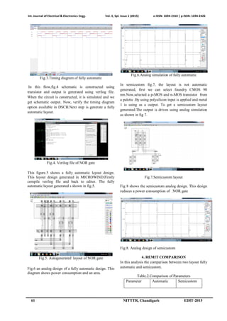
![Int. Journal of Electrical & Electronics Engg. Vol. 2, Spl. Issue 1 (2015) e-ISSN: 1694-2310 | p-ISSN: 1694-2426
NITTTR, Chandigarh EDIT -2015 62
1.Area 26.2µm 8.5 µm
2.Power 1.943 µw 1.037 µw
This bar graph represents the reduction of power and
area.
5. CONCLUSION
In this paper of presents fully automatic design and
Semi-custom design to optimize area and power in VLSI
design. Layout of NOR gate has been designed and
simulated using above mentioned techniques for area
and power comparison both the layouts have been
simulated using 90 nm technology. The simulated
results show that semicustom techniques based NOR
layout consumes 8.5µm2
area as compared to 26.2µm2
is
case of fully automatic NOR gate. It can not also be
observed from simulated results that semicustom NOR
gate consume 1.037µw power as a compared to 1.943
µw in case of fully automatic NOR gate.Semicustom
design reduces the area and power.The area and power
performance is improved in semicustom design. Area is
reduced by 67% and power consumption is reduced by
46%.
REFERENCES
[1] Tanvi Sood, Rajesh Mehra,“IOSR Journal of VLSI and
processing” volume 2, Issue(3 May-June13) .
[2] Pooja Singh, Rajesh Mehra, “Advances in electrical and
information communication technology” Nationl Student
Conference, AEICT-2014.
[3] Pushpa Saini, “Leakage power reduction in CMOS VLSI
circuits”Internationl Journal of Computer Applications,PP
No.8,Vol.55, October 2012.
[4] Srinivara Rao.Ijjada, Raghaanandra sirigiri, B.S.N.S.P kumar,
V.Malleswala Rao, “Design of high efficient and Low power
basic gates in subthreshold region”.
[5] Vibha Soni, Nittin Naiyar, “Evaluation of Logic families
using NOR and NAND Logic gates “International Journal of
Engineering and Innovative Technology(IJEIT), Volume
3,Issue 7,January 2014.
[6] Neil Weste and David Harris, CMOS VLSI Design, Circuit
and system perspective, page number8.Edition 3.
[7] Shobha sharma1
,Ashawani kumar2
,Nupur prakash 3
,B.V.R.
reddy, “High Speed Metal Gate strained Si CMOS NOR
gate”Inernational journal of Emerging Technology and
Advanced Emerging (ISSN2250-2459,ISO 900l:2008
certified Journal, Volume 3,Issue 7, July 2013.
ACKNOWLEDGEMENT
I would like to express my thanks to my supportive
teacher who gave me such opportunity to do a this
wonderful research work on the Low Power
Consumption and Implementation of nor gate, which
also helped me doing a lot of researches and I came to
know about so many new things](https://image.slidesharecdn.com/id43-150525185406-lva1-app6892/85/Layout-Design-Implementation-of-NOR-Gate-3-320.jpg)

This document discusses the design and implementation of a CMOS NOR gate using VLSI technology, highlighting the reduction of power consumption by 46% and area by 67%. It compares two design flows: fully automatic and semicustom, with the latter proving to be more efficient. The results indicate that the semicustom design significantly optimizes both area and power in integrated circuit applications.

![RF Module Design - [Chapter 7] Voltage-Controlled Oscillator](https://cdn.slidesharecdn.com/ss_thumbnails/rfch7-150613070347-lva1-app6892-thumbnail.jpg?width=640&height=640&fit=bounds)


![RF Circuit Design - [Ch2-1] Resonator and Impedance Matching](https://cdn.slidesharecdn.com/ss_thumbnails/ch2-1-150613064353-lva1-app6892-thumbnail.jpg?width=640&height=640&fit=bounds)


![RF Circuit Design - [Ch3-2] Power Waves and Power-Gain Expressions](https://cdn.slidesharecdn.com/ss_thumbnails/ch3-2-150613064404-lva1-app6891-thumbnail.jpg?width=640&height=640&fit=bounds)