Downloaded 12 times
![Prakash.T.Patil Int. Journal of Engineering Research and Applications www.ijera.com
ISSN : 2248-9622, Vol. 5, Issue 4, ( Part -7) April 2015, pp.129-133
www.ijera.com 129 | P a g e
Multilevel Inverter using SPWM Technique for AC Power Supply
Prakash.T.Patil*, Sagar.S.Pawar**
*(Department of Electronics and Telecommunication, Jayawantrao Sawant College of Engineering, University
of Pune, Pune-411028)
** (Department of electronics & Telecommunication, Jayawantrao Sawant College of Engineering, University
of Pune, Pune-411028)
ABSTRACT
This paper presents two multilevel inverter for AC power supply. The cascaded H bridge topology of multilevel
inverter is implemented .The control strategy has been design using SPWM technique. The operation of
multilevel inverter is analyzed. The output has controlled and reduction in harmonic and THD. The simulation
model has been built in matlab simulink and results are observed.
Keywords – Bi directional switch, multilevel inverter, matlab simulink, spwm,
I. Introduction
In the recent years the demand for high-voltage
high-power is increasing in the industrial applications
.The requirement of medium voltage and megawatt
power level were require for the medium voltage
motor drives and utility applications. So there was
problem to connect only single power semiconductor
switch directly to a medium voltage grid. As an
alternative in high power and medium voltage
situations a multilevel inverter structure had been
introduced. From the multiple voltage levels with less
distortion, less switching frequency, higher
efficiency, and lower voltage devices a synthesize
output voltage waveform can be desired. There exits
different types of multilevel inverter. The different
types of multilevel inverter topologies are as follows
1. The diode clamped or neutral point clamped
(NPC) [1] ,
2. The capacitor clamped or flying capacitor (FC)
[2]
3. The cascaded H-bridge (CHB)[3].
The NPC uses the diode clamped on the input
side of the inverter but the main drawbacks of diode
clamped topology is the unequal voltage sharing
among series connected capacitors. The FC
multilevel inverter uses flying capacitor as clamping
devices. These topologies have several advantages in
comparison with the NPC inverter, including the
advantage of the transformer less function and
unnecessary phase leg states that allow the switching
stresses to be equally distributed between
semiconductor switches [4],[5].But, these inverters
require an excessive number of storage capacitors for
higher voltage steps. In FC multilevel inverter if any
of the internal module is faulty then the maximum
output voltage remains constant, but the number of
levels decreases. It is noticeable that multilevel
inverters can sustain the operation in case of internal
fault [6]. For high level applications and for good
modularity and simplicity of control the CHB
topologies are good option. In this topology, a large
number of isolated dc voltage sources are required to
supply each conversion module. It increases the
inverter cost and complexity. However, it causes to
the increasing number of switching devices and other
components, and increases the cost and control
complexity and tends to reduce the overall reliability
and efficiency of the inverter. In the CHB inverter if
an internal fault is detected and that faulty module is
identified, it can be easily isolated through an
external switch and replaced by a new operative
module [7]. In the proposed system the modules are
cascaded in the series connection. The output
obtained in the proposed system is of high efficiency
and the harmonics are also reduced. The strategy
used in the proposed system is SPWM which is easy
to control and thus obtained a high efficiency output.
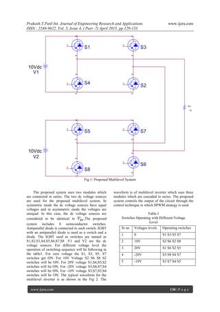
II. Proposed System
Fig (1) shows the proposed multilevel system.
RESEARCH ARTICLE OPEN ACCESS](https://image.slidesharecdn.com/w50407129133-150501062722-conversion-gate01/85/Multilevel-Inverter-using-SPWM-Technique-for-AC-Power-Supply-1-320.jpg)
![Prakash.T.Patil Int. Journal of Engineering Research and Applications www.ijera.com
ISSN : 2248-9622, Vol. 5, Issue 4, ( Part -7) April 2015, pp.129-133
www.ijera.com 129 | P a g e
Multilevel Inverter using SPWM Technique for AC Power Supply
Prakash.T.Patil*, Sagar.S.Pawar**
*(Department of Electronics and Telecommunication, Jayawantrao Sawant College of Engineering, University
of Pune, Pune-411028)
** (Department of electronics & Telecommunication, Jayawantrao Sawant College of Engineering, University
of Pune, Pune-411028)
ABSTRACT
This paper presents two multilevel inverter for AC power supply. The cascaded H bridge topology of multilevel
inverter is implemented .The control strategy has been design using SPWM technique. The operation of
multilevel inverter is analyzed. The output has controlled and reduction in harmonic and THD. The simulation
model has been built in matlab simulink and results are observed.
Keywords – Bi directional switch, multilevel inverter, matlab simulink, spwm,
I. Introduction
In the recent years the demand for high-voltage
high-power is increasing in the industrial applications
.The requirement of medium voltage and megawatt
power level were require for the medium voltage
motor drives and utility applications. So there was
problem to connect only single power semiconductor
switch directly to a medium voltage grid. As an
alternative in high power and medium voltage
situations a multilevel inverter structure had been
introduced. From the multiple voltage levels with less
distortion, less switching frequency, higher
efficiency, and lower voltage devices a synthesize
output voltage waveform can be desired. There exits
different types of multilevel inverter. The different
types of multilevel inverter topologies are as follows
1. The diode clamped or neutral point clamped
(NPC) [1] ,
2. The capacitor clamped or flying capacitor (FC)
[2]
3. The cascaded H-bridge (CHB)[3].
The NPC uses the diode clamped on the input
side of the inverter but the main drawbacks of diode
clamped topology is the unequal voltage sharing
among series connected capacitors. The FC
multilevel inverter uses flying capacitor as clamping
devices. These topologies have several advantages in
comparison with the NPC inverter, including the
advantage of the transformer less function and
unnecessary phase leg states that allow the switching
stresses to be equally distributed between
semiconductor switches [4],[5].But, these inverters
require an excessive number of storage capacitors for
higher voltage steps. In FC multilevel inverter if any
of the internal module is faulty then the maximum
output voltage remains constant, but the number of
levels decreases. It is noticeable that multilevel
inverters can sustain the operation in case of internal
fault [6]. For high level applications and for good
modularity and simplicity of control the CHB
topologies are good option. In this topology, a large
number of isolated dc voltage sources are required to
supply each conversion module. It increases the
inverter cost and complexity. However, it causes to
the increasing number of switching devices and other
components, and increases the cost and control
complexity and tends to reduce the overall reliability
and efficiency of the inverter. In the CHB inverter if
an internal fault is detected and that faulty module is
identified, it can be easily isolated through an
external switch and replaced by a new operative
module [7]. In the proposed system the modules are
cascaded in the series connection. The output
obtained in the proposed system is of high efficiency
and the harmonics are also reduced. The strategy
used in the proposed system is SPWM which is easy
to control and thus obtained a high efficiency output.
II. Proposed System
Fig (1) shows the proposed multilevel system.
RESEARCH ARTICLE OPEN ACCESS](https://image.slidesharecdn.com/w50407129133-150501062722-conversion-gate01/75/Multilevel-Inverter-using-SPWM-Technique-for-AC-Power-Supply-1-2048.jpg)
![Prakash.T.Patil Int. Journal of Engineering Research and Applications www.ijera.com
ISSN : 2248-9622, Vol. 5, Issue 4, ( Part -7) April 2015, pp.129-133
www.ijera.com 133 | P a g e
Fig 5(c) input 50 and 20 Vdc and output 70 V
Fig 6: Output of SPWM
VI. Conclusion
The multilevel inverter with single phase and
different DC voltage sources has been built. The
output of the multilevel inverter is the sum of the
output of each module. The proposed system has
been successfully built in the matlab and has
simulated in matlab. The expected results have been
obtained. As the output obtained shows reduction in
harmonics and THD.
REFERENCES
[1] A. Nabae, I. Takahashi, and H. Akagi, “A
new neutral-point-clamped PWM inverter,”
IEEE Trans. Ind. Appl., vol. IA-17, no. 5,
pp. 518 523,Sep. 1981.
[2] T. A. Meynard and H. Foch, “Multi-level
choppers for high voltage applications,” in
Proc Eur.Conf. Power Electron. Appl.,
1992, vol. 2, pp. 45–50.
[3] M. Marchesoni, M. Mazzucchelli, and S.
Tenconi, “A non conventional power
converter for plasma stabilization,” in Proc.
Power Electron.
Spec. Conf., 1988, pp. 122–129.
[4] S. S. Fazel, S. Bernet, D. Krug, and K. Jalili,
“Design and comparison of 4-kV neutral-
point-clamped, flying-capacitor, and series-
connected H-bridge multilevel converters,”
IEEE Trans. Ind. Appl., vol. 43, no. 4, pp.
1032–1040, Jul./Aug. 2007.
[5] B. P. McGrath and D. G. Holmes,
“Analytical modelling of voltage balance
dynamics for a flying capacitor multilevel
converter,” IEEE Trans. Power Electron.
vol. 23, no. 2, pp. 543–550, Mar. 2008.
[6] P. Lezana, J. Pou, T. A. Meynard, J.
Rodriguez, S. Ceballos, and F. Richardeau,
“Survey on fault operation on multilevel
inverters,” IEEE Trans. Ind. Electron, vol.
57, no. 7, pp. 2207 2218, Jul. 2010.
[7] A. K. Sadigh, S. H. Hosseini, M. Sabahi,
and G. B. Gharehpetian, “Double flying
capacitor multicell converter based on
modified phase-shifted pulsewidth
modulation,” IEEE Trans. Power Electron.
vol. 25, no. 6, pp. 1517–1526, Jun. 2010.](https://image.slidesharecdn.com/w50407129133-150501062722-conversion-gate01/85/Multilevel-Inverter-using-SPWM-Technique-for-AC-Power-Supply-5-320.jpg)

This paper discusses the implementation of a multilevel inverter using a cascaded H-bridge topology along with a sinusoidal pulse width modulation (SPWM) technique to control AC power supply. The proposed system, which employs eight semiconductor switches and operates under various DC voltage inputs, yields outputs with reduced harmonics and improved efficiency. Simulation results obtained in MATLAB demonstrate effective performance, confirming the system's reliability and output quality.


![6.[36 45]seven level modified cascaded inverter for induction motor drive app...](https://cdn.slidesharecdn.com/ss_thumbnails/6-36-45sevenlevelmodifiedcascadedinverterforinductionmotordriveapplications-111118182704-phpapp01-thumbnail.jpg?width=640&height=640&fit=bounds)


