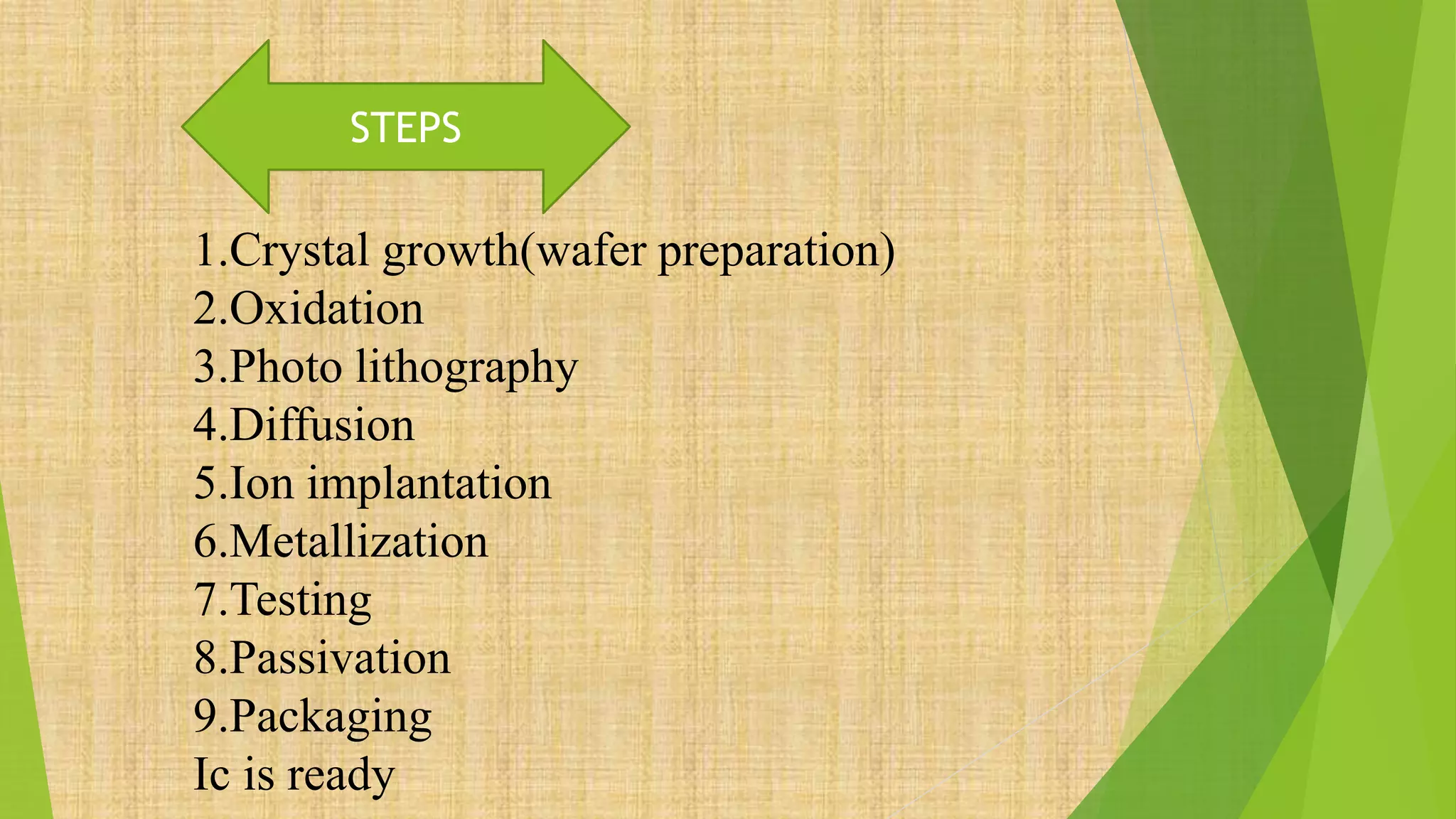
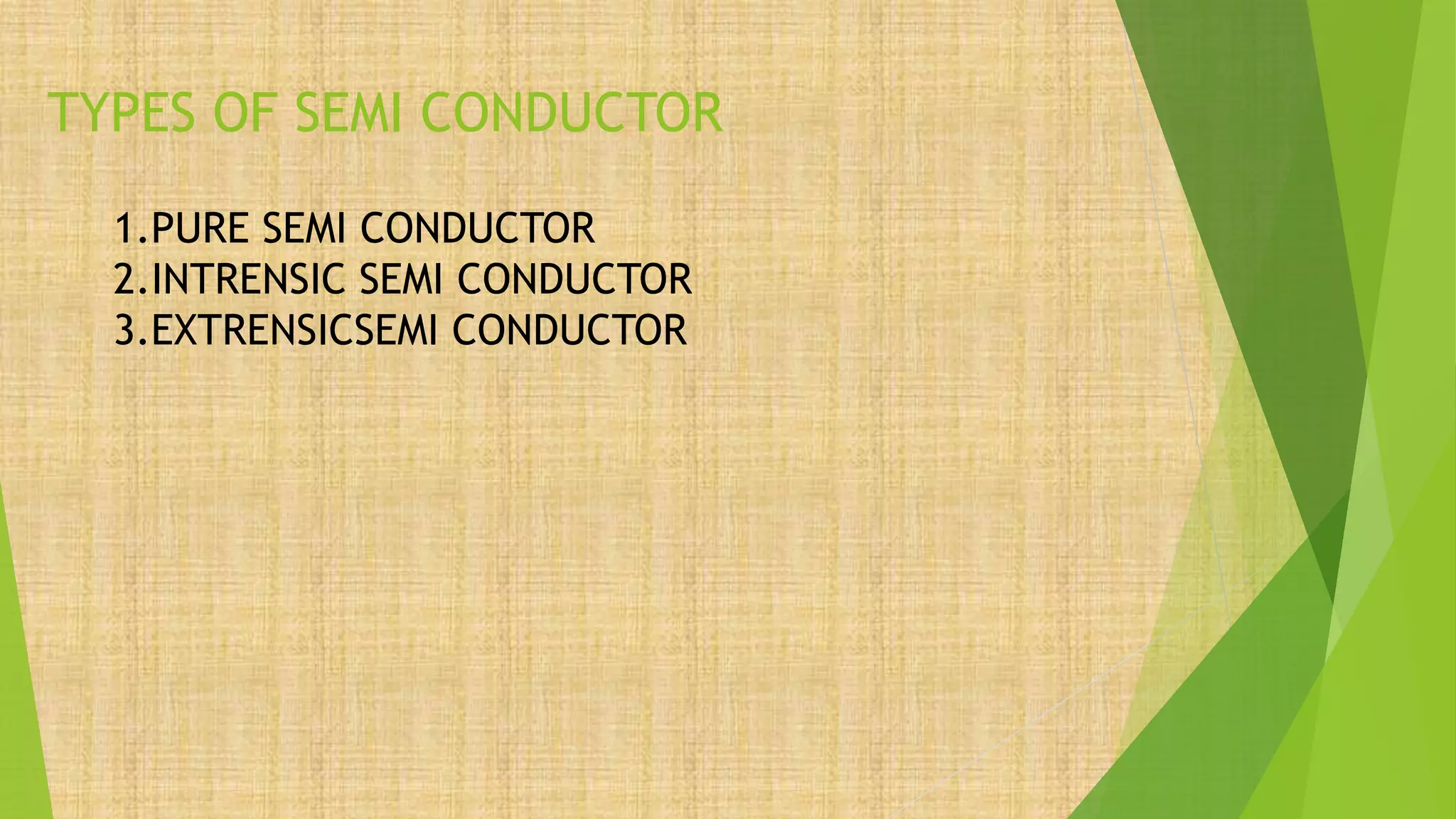
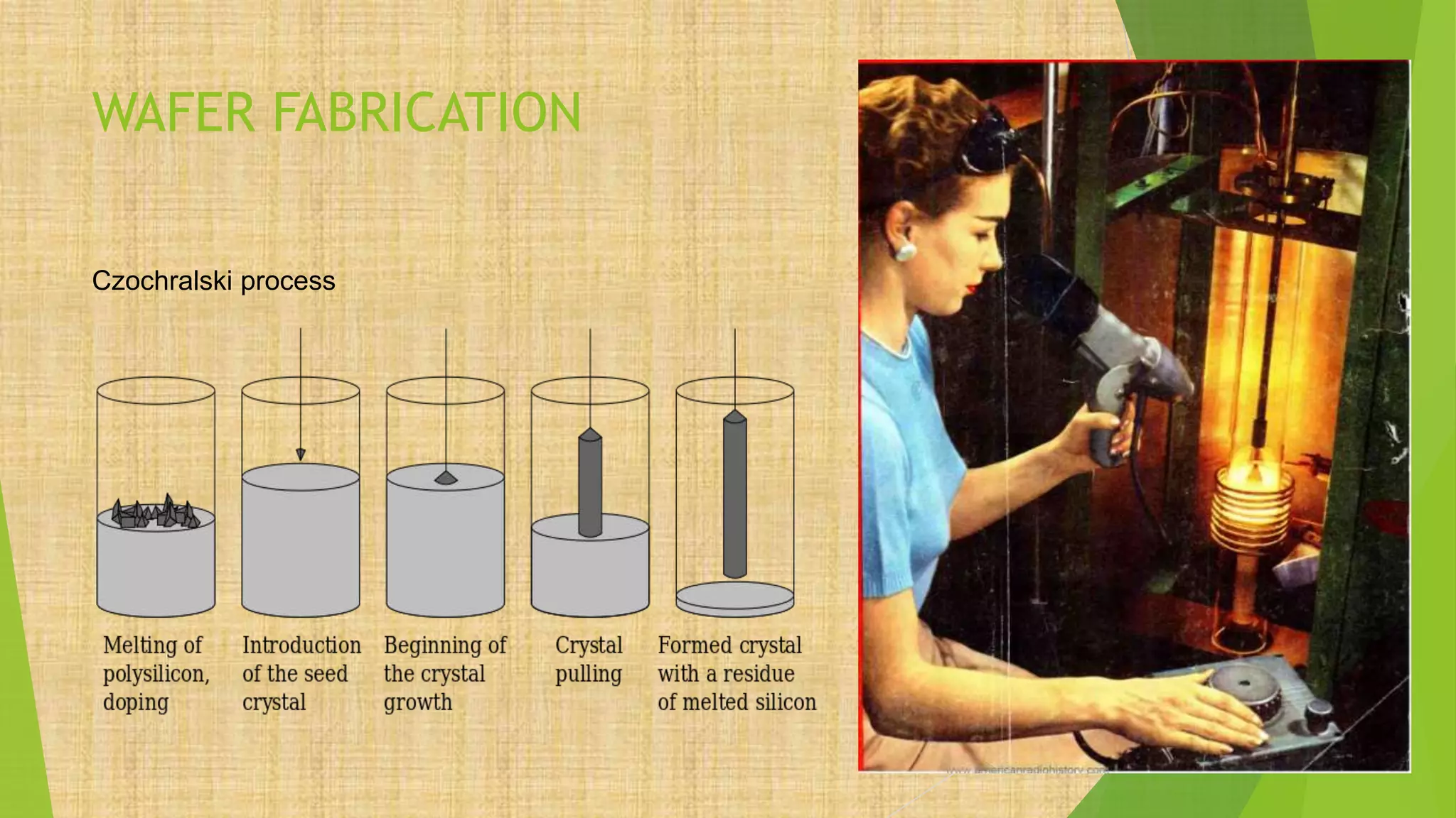
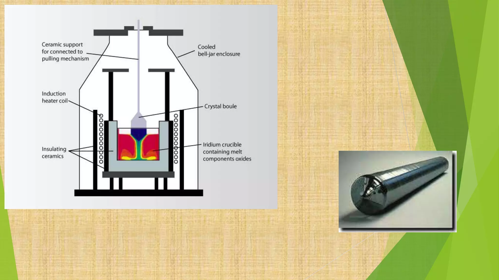
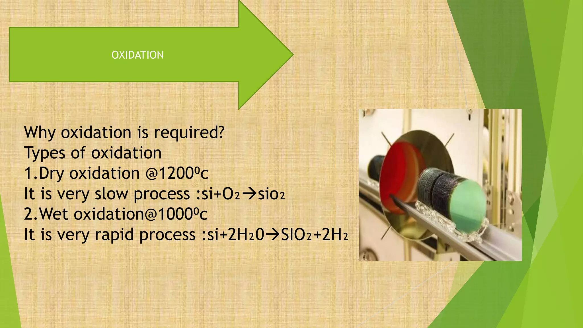
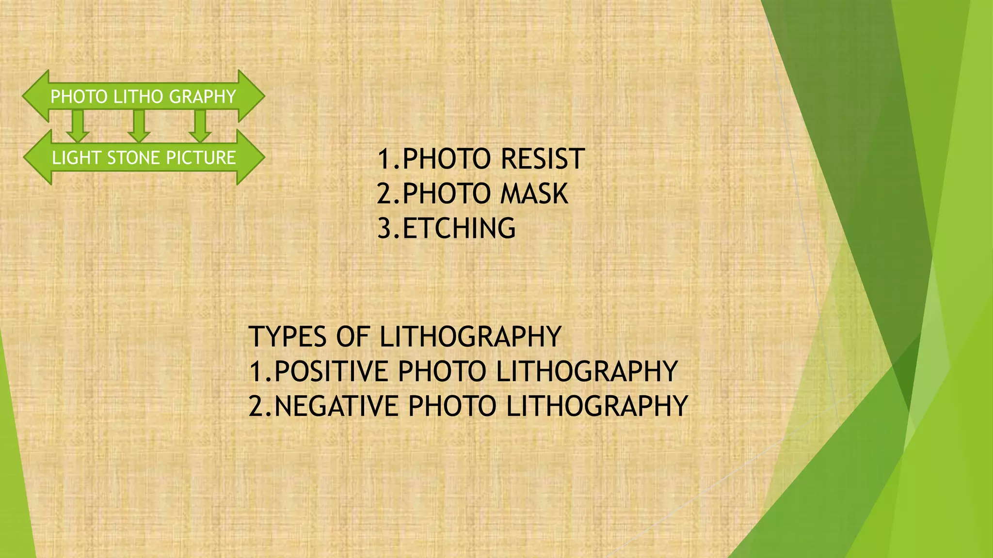
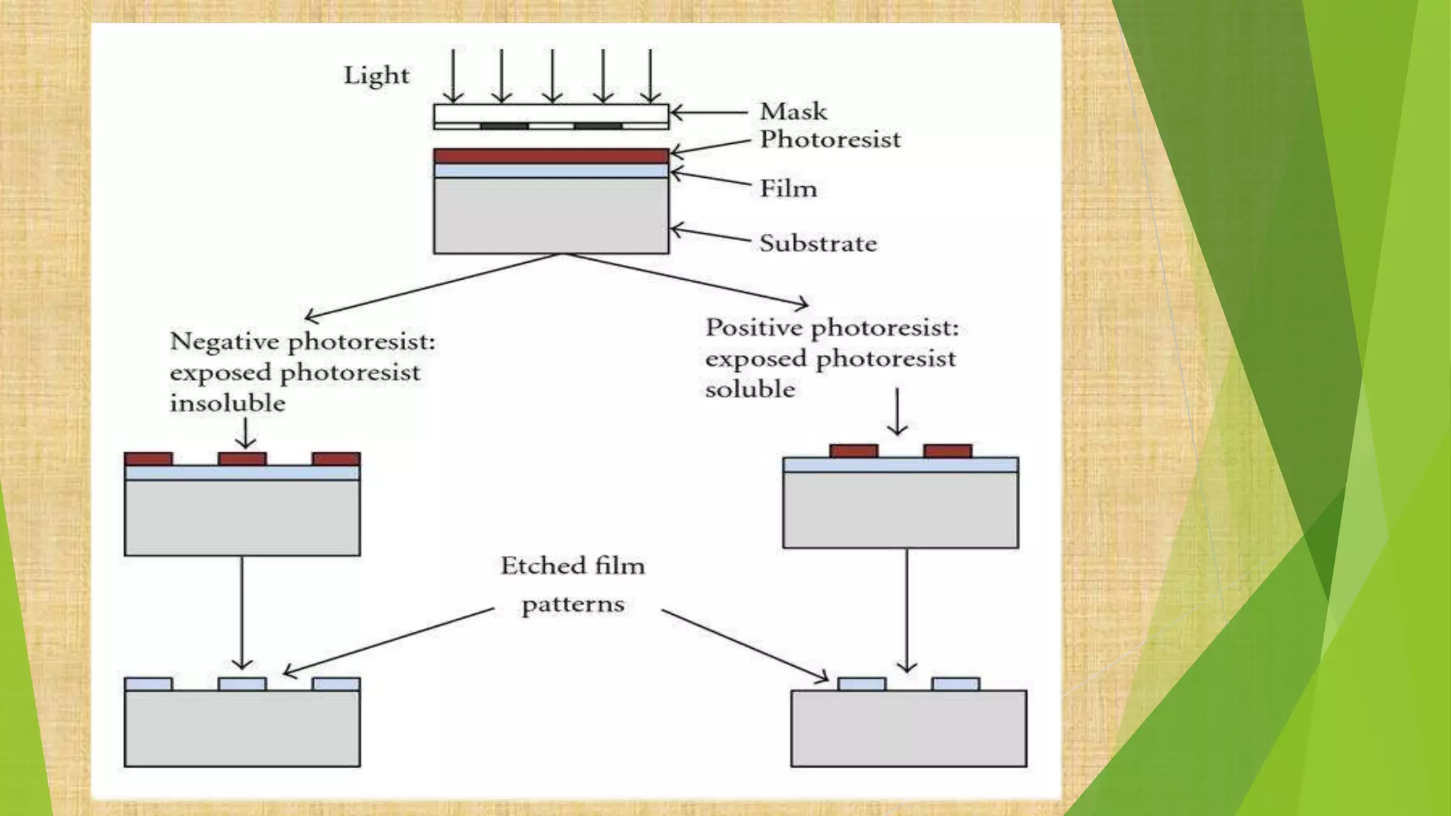
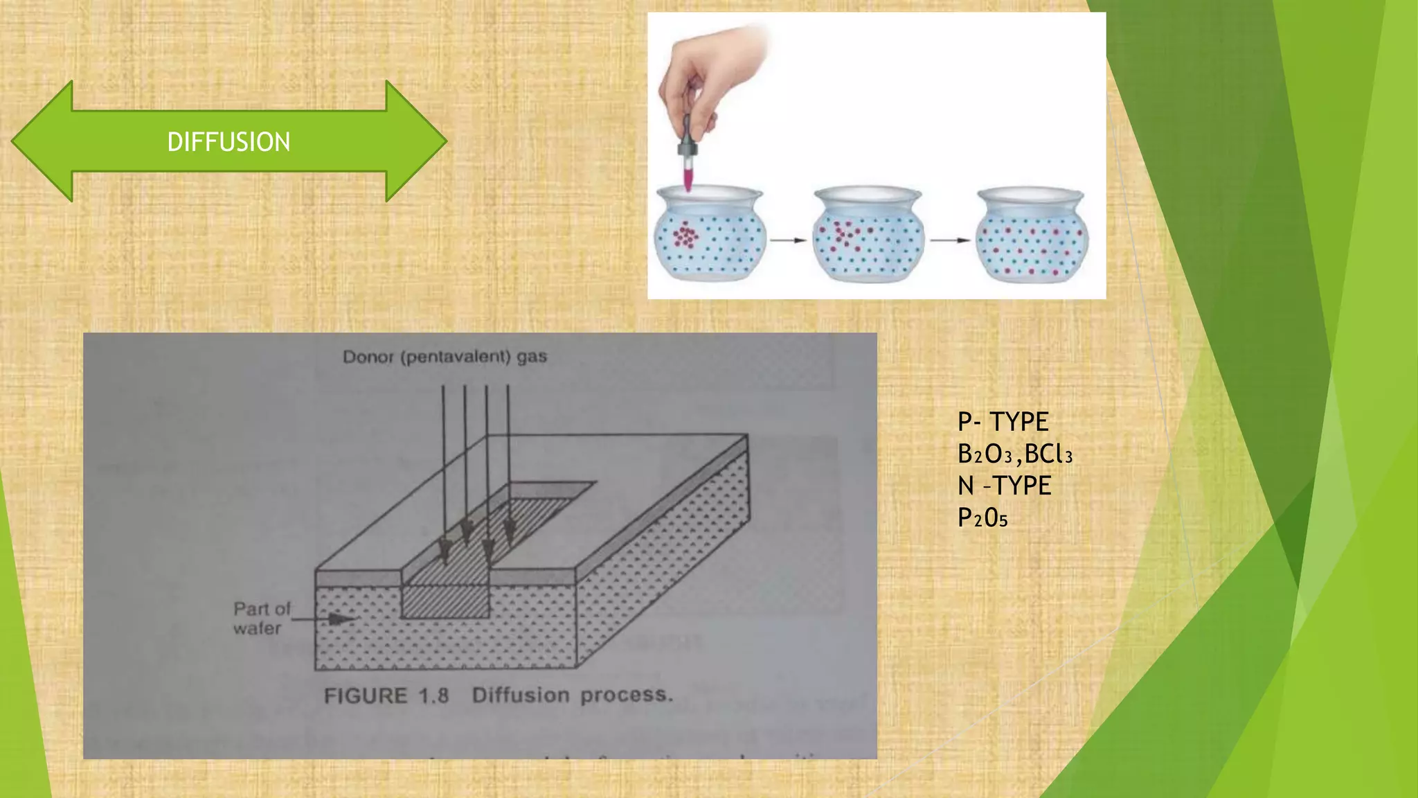
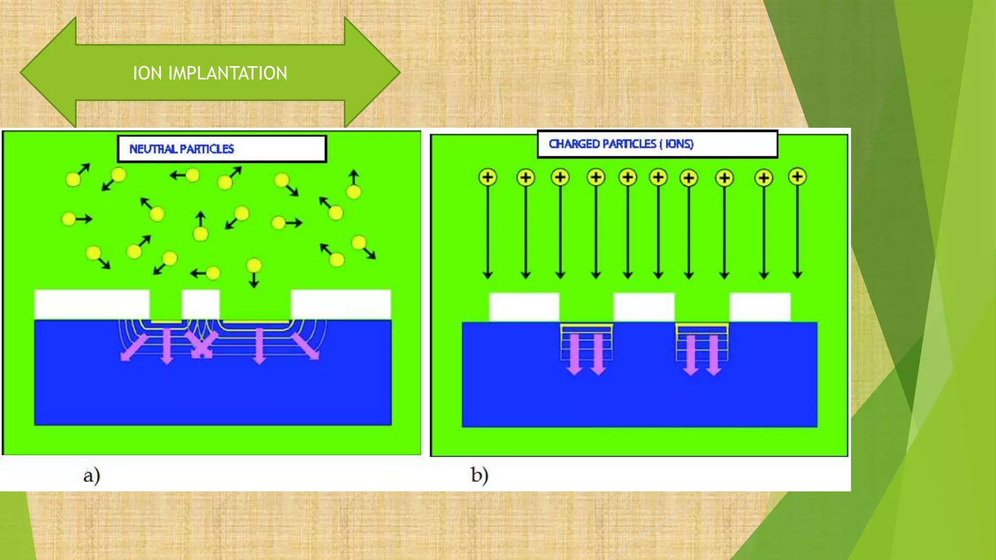
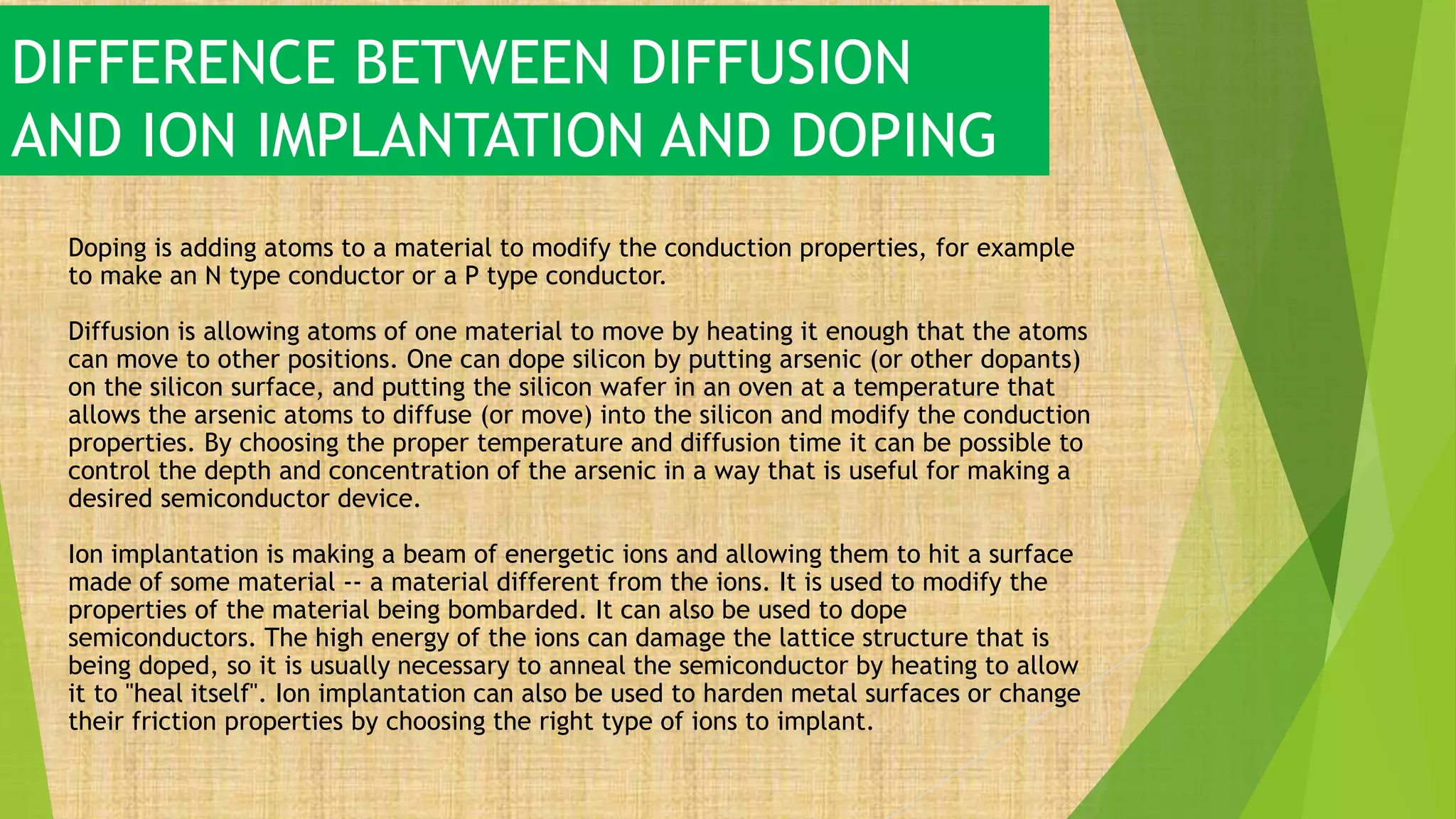
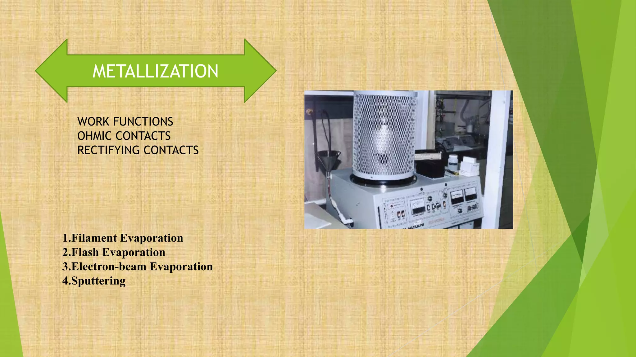
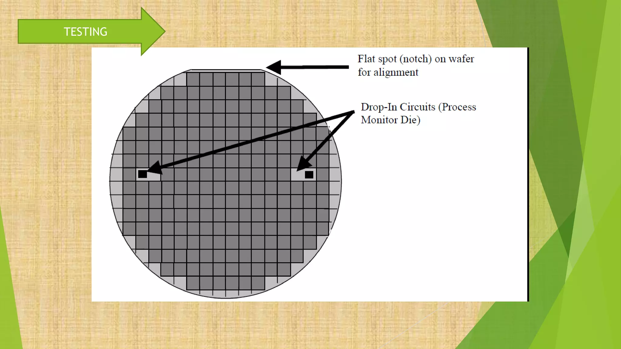
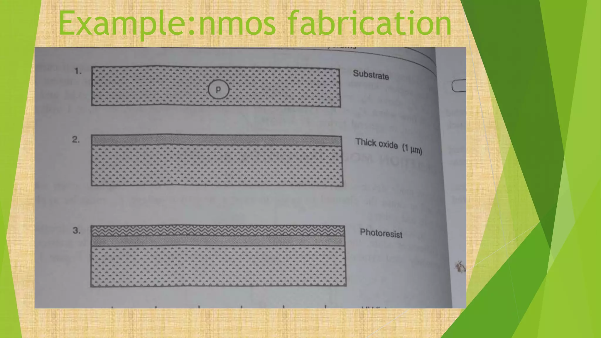
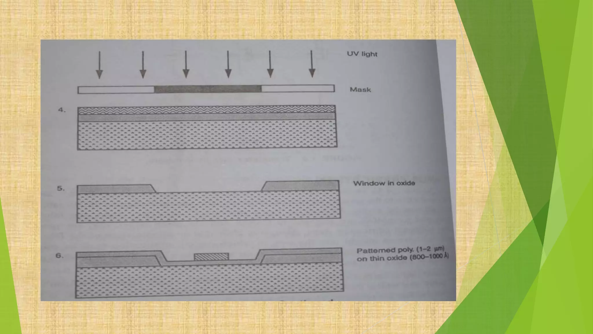
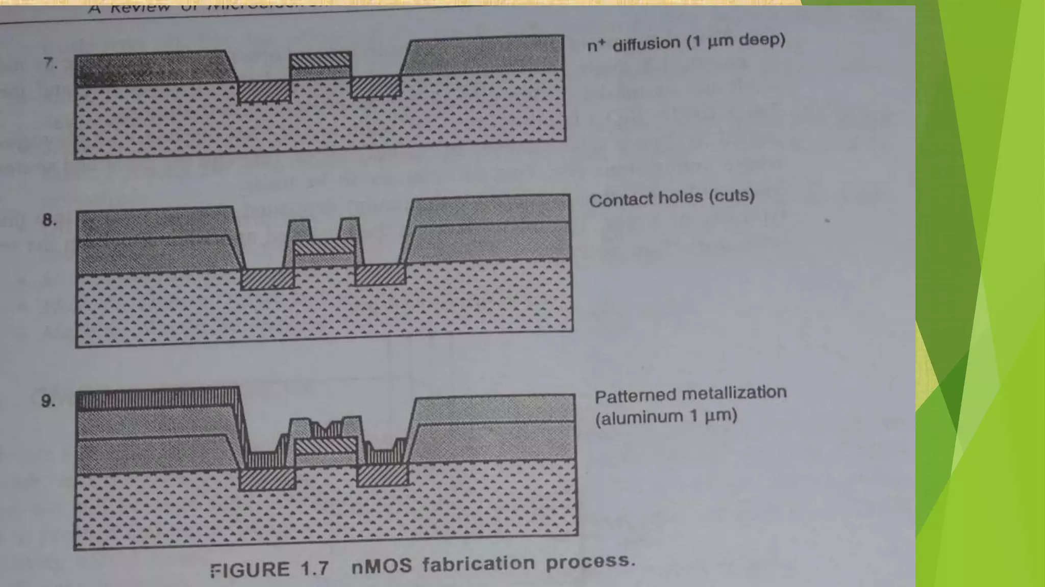
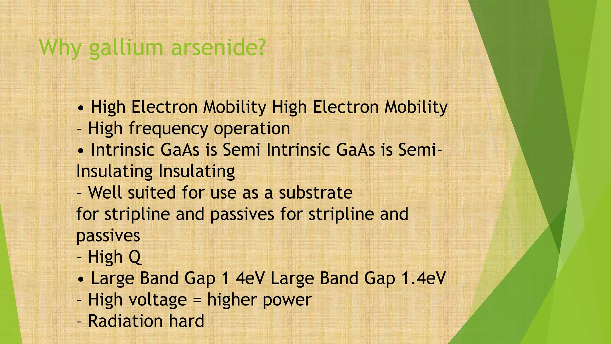
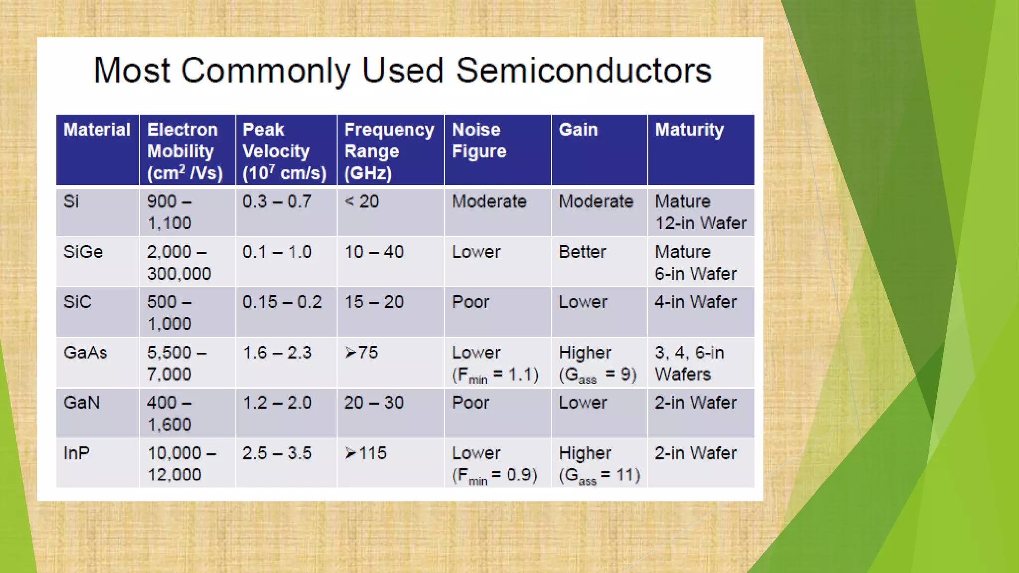
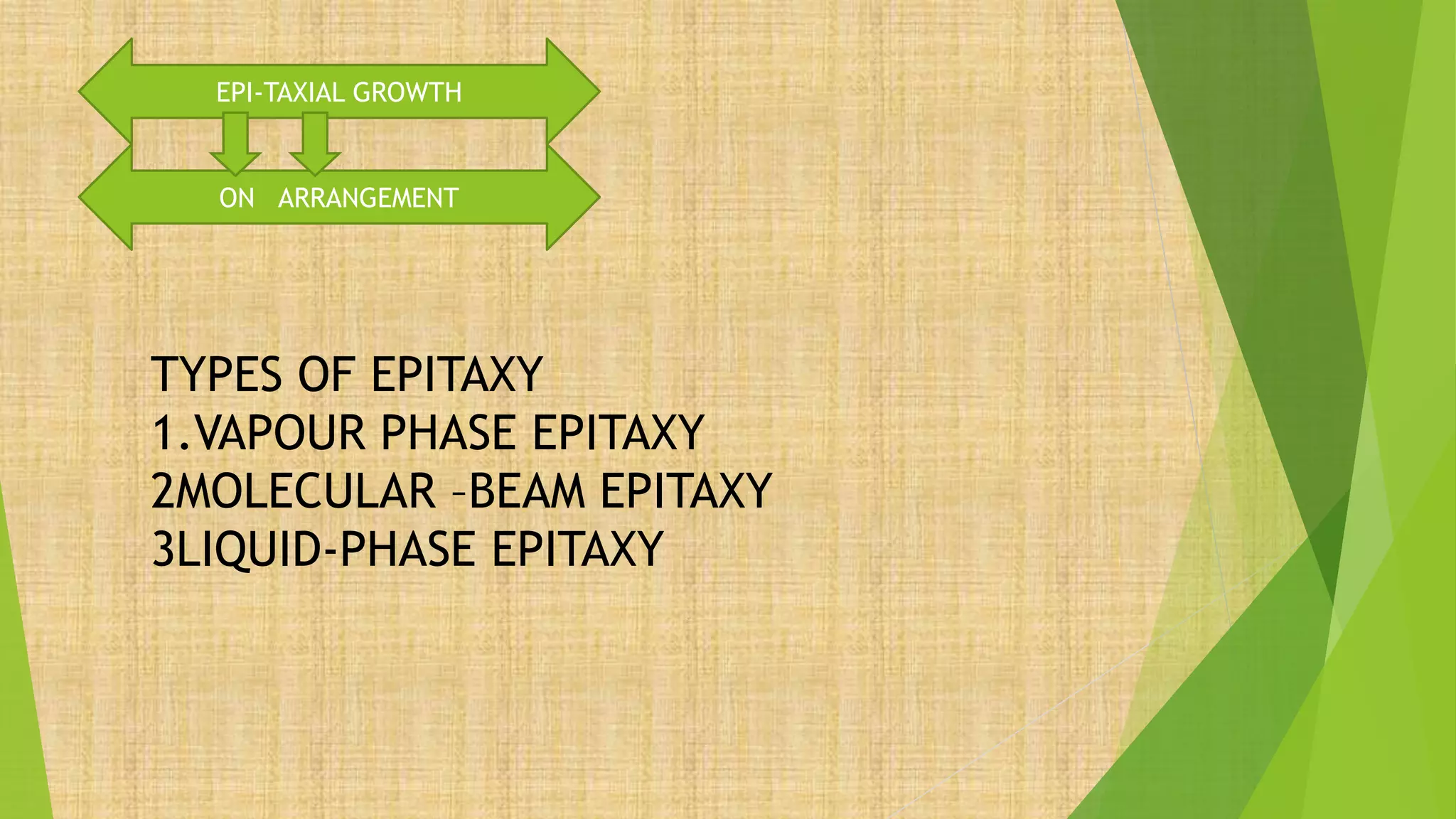
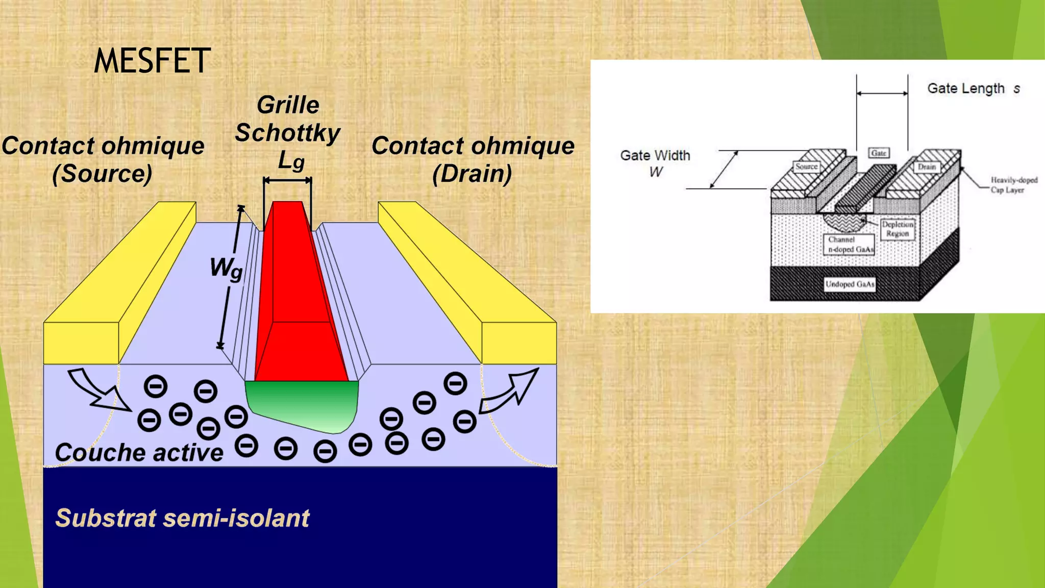
IC FABRICATION
BY
BHAVANA.POTTURI
STEPS
1.Crystal growth(wafer preparation)
2.Oxidation
3.Photo lithography
4.Diffusion
5.Ion implantation
6.Metallization
7.Testing
8.Passivation
9.Packaging
Ic is ready
TYPES OF SEMI CONDUCTOR
1.PURE SEMI CONDUCTOR
2.INTRENSIC SEMI CONDUCTOR
3.EXTRENSICSEMI CONDUCTOR
WAFER FABRICATION
Czochralski process
APPARATUS
OXIDATION
Why oxidation is required?
Types of oxidation
1.Dry oxidation @1200⁰c
It is very slow process :si+O₂sio₂
2.Wet oxidation@1000⁰c
It is very rapid process :si+2H₂0SIO₂+2H₂
PHOTO LITHO GRAPHY
LIGHT STONE PICTURE 1.PHOTO RESIST
2.PHOTO MASK
3.ETCHING
TYPES OF LITHOGRAPHY
1.POSITIVE PHOTO LITHOGRAPHY
2.NEGATIVE PHOTO LITHOGRAPHY
DIFFUSION
P- TYPE
B₂O₃,BCl₃
N –TYPE
P₂0₅
ION IMPLANTATION
DIFFERENCE BETWEEN DIFFUSION
AND ION IMPLANTATION AND DOPING
Doping is adding atoms to a material to modify the conduction properties, for example
to make an N type conductor or a P type conductor.
Diffusion is allowing atoms of one material to move by heating it enough that the atoms
can move to other positions. One can dope silicon by putting arsenic (or other dopants)
on the silicon surface, and putting the silicon wafer in an oven at a temperature that
allows the arsenic atoms to diffuse (or move) into the silicon and modify the conduction
properties. By choosing the proper temperature and diffusion time it can be possible to
control the depth and concentration of the arsenic in a way that is useful for making a
desired semiconductor device.
Ion implantation is making a beam of energetic ions and allowing them to hit a surface
made of some material -- a material different from the ions. It is used to modify the
properties of the material being bombarded. It can also be used to dope
semiconductors. The high energy of the ions can damage the lattice structure that is
being doped, so it is usually necessary to anneal the semiconductor by heating to allow
it to "heal itself". Ion implantation can also be used to harden metal surfaces or change
their friction properties by choosing the right type of ions to implant.
METALLIZATION
WORK FUNCTIONS
OHMIC CONTACTS
RECTIFYING CONTACTS
1.Filament Evaporation
2.Flash Evaporation
3.Electron-beam Evaporation
4.Sputtering
TESTING
PASSIVATION
PACKAGING
Example:nmos fabrication
Why gallium arsenide?
• High Electron Mobility High Electron Mobility
– High frequency operation
• Intrinsic GaAs is Semi Intrinsic GaAs is Semi-
Insulating Insulating
– Well suited for use as a substrate
for stripline and passives for stripline and
passives
– High Q
• Large Band Gap 1 4eV Large Band Gap 1.4eV
– High voltage = higher power
– Radiation hard
EPI-TAXIAL GROWTH
ON ARRANGEMENT
TYPES OF EPITAXY
1.VAPOUR PHASE EPITAXY
2MOLECULAR –BEAM EPITAXY
3LIQUID-PHASE EPITAXY
MESFET
Any queries?
FEEDBACK
New microsoft power point presentation

New microsoft power point presentation

  • 1.
  • 2.
    STEPS 1.Crystal growth(wafer preparation) 2.Oxidation 3.Photolithography 4.Diffusion 5.Ion implantation 6.Metallization 7.Testing 8.Passivation 9.Packaging Ic is ready
  • 3.
    TYPES OF SEMICONDUCTOR 1.PURE SEMI CONDUCTOR 2.INTRENSIC SEMI CONDUCTOR 3.EXTRENSICSEMI CONDUCTOR
  • 4.
  • 5.
  • 6.
    OXIDATION Why oxidation isrequired? Types of oxidation 1.Dry oxidation @1200⁰c It is very slow process :si+O₂sio₂ 2.Wet oxidation@1000⁰c It is very rapid process :si+2H₂0SIO₂+2H₂
  • 7.
    PHOTO LITHO GRAPHY LIGHTSTONE PICTURE 1.PHOTO RESIST 2.PHOTO MASK 3.ETCHING TYPES OF LITHOGRAPHY 1.POSITIVE PHOTO LITHOGRAPHY 2.NEGATIVE PHOTO LITHOGRAPHY
  • 9.
  • 10.
  • 11.
    DIFFERENCE BETWEEN DIFFUSION ANDION IMPLANTATION AND DOPING Doping is adding atoms to a material to modify the conduction properties, for example to make an N type conductor or a P type conductor. Diffusion is allowing atoms of one material to move by heating it enough that the atoms can move to other positions. One can dope silicon by putting arsenic (or other dopants) on the silicon surface, and putting the silicon wafer in an oven at a temperature that allows the arsenic atoms to diffuse (or move) into the silicon and modify the conduction properties. By choosing the proper temperature and diffusion time it can be possible to control the depth and concentration of the arsenic in a way that is useful for making a desired semiconductor device. Ion implantation is making a beam of energetic ions and allowing them to hit a surface made of some material -- a material different from the ions. It is used to modify the properties of the material being bombarded. It can also be used to dope semiconductors. The high energy of the ions can damage the lattice structure that is being doped, so it is usually necessary to anneal the semiconductor by heating to allow it to "heal itself". Ion implantation can also be used to harden metal surfaces or change their friction properties by choosing the right type of ions to implant.
  • 12.
    METALLIZATION WORK FUNCTIONS OHMIC CONTACTS RECTIFYINGCONTACTS 1.Filament Evaporation 2.Flash Evaporation 3.Electron-beam Evaporation 4.Sputtering
  • 13.
  • 14.
  • 15.
  • 18.
    Why gallium arsenide? •High Electron Mobility High Electron Mobility – High frequency operation • Intrinsic GaAs is Semi Intrinsic GaAs is Semi- Insulating Insulating – Well suited for use as a substrate for stripline and passives for stripline and passives – High Q • Large Band Gap 1 4eV Large Band Gap 1.4eV – High voltage = higher power – Radiation hard
  • 21.
    EPI-TAXIAL GROWTH ON ARRANGEMENT TYPESOF EPITAXY 1.VAPOUR PHASE EPITAXY 2MOLECULAR –BEAM EPITAXY 3LIQUID-PHASE EPITAXY
  • 22.
  • 23.