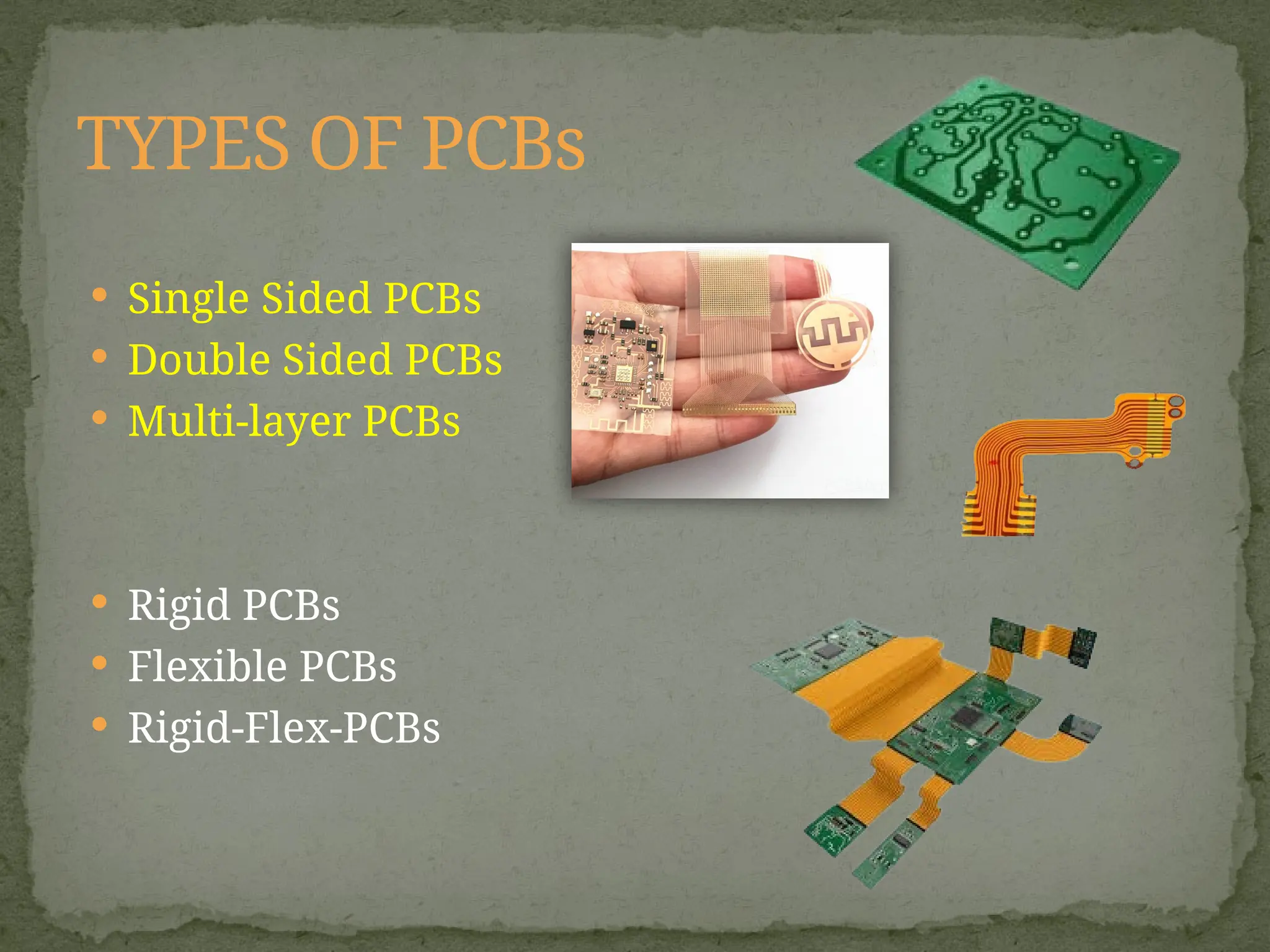
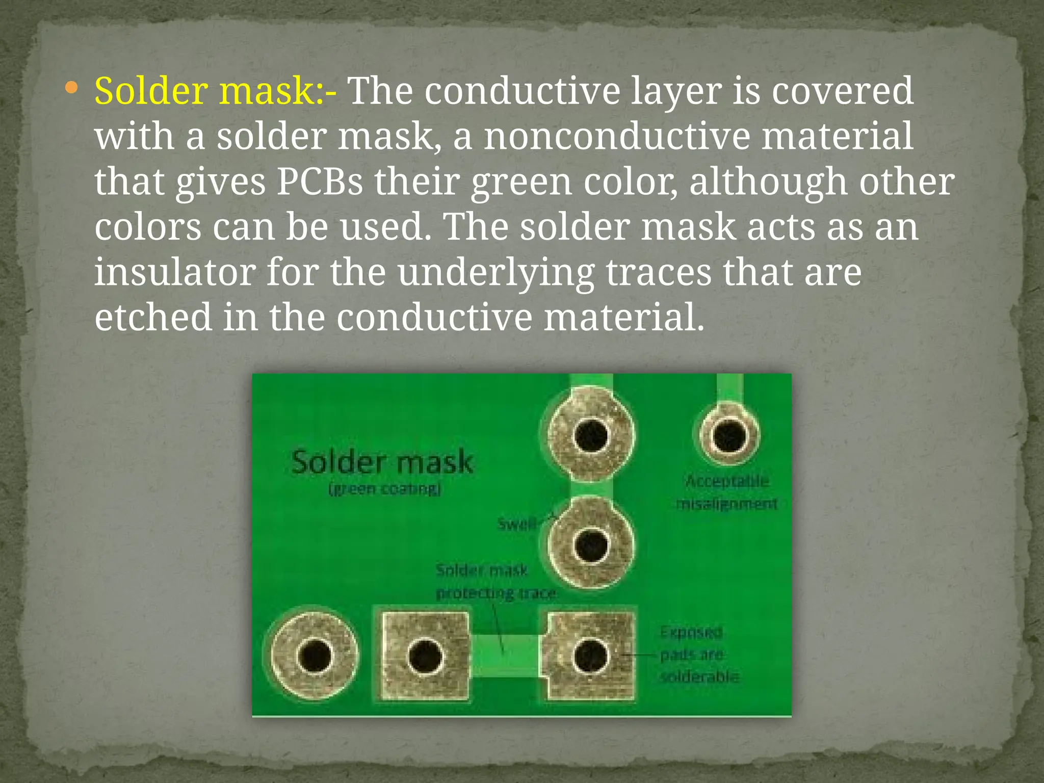
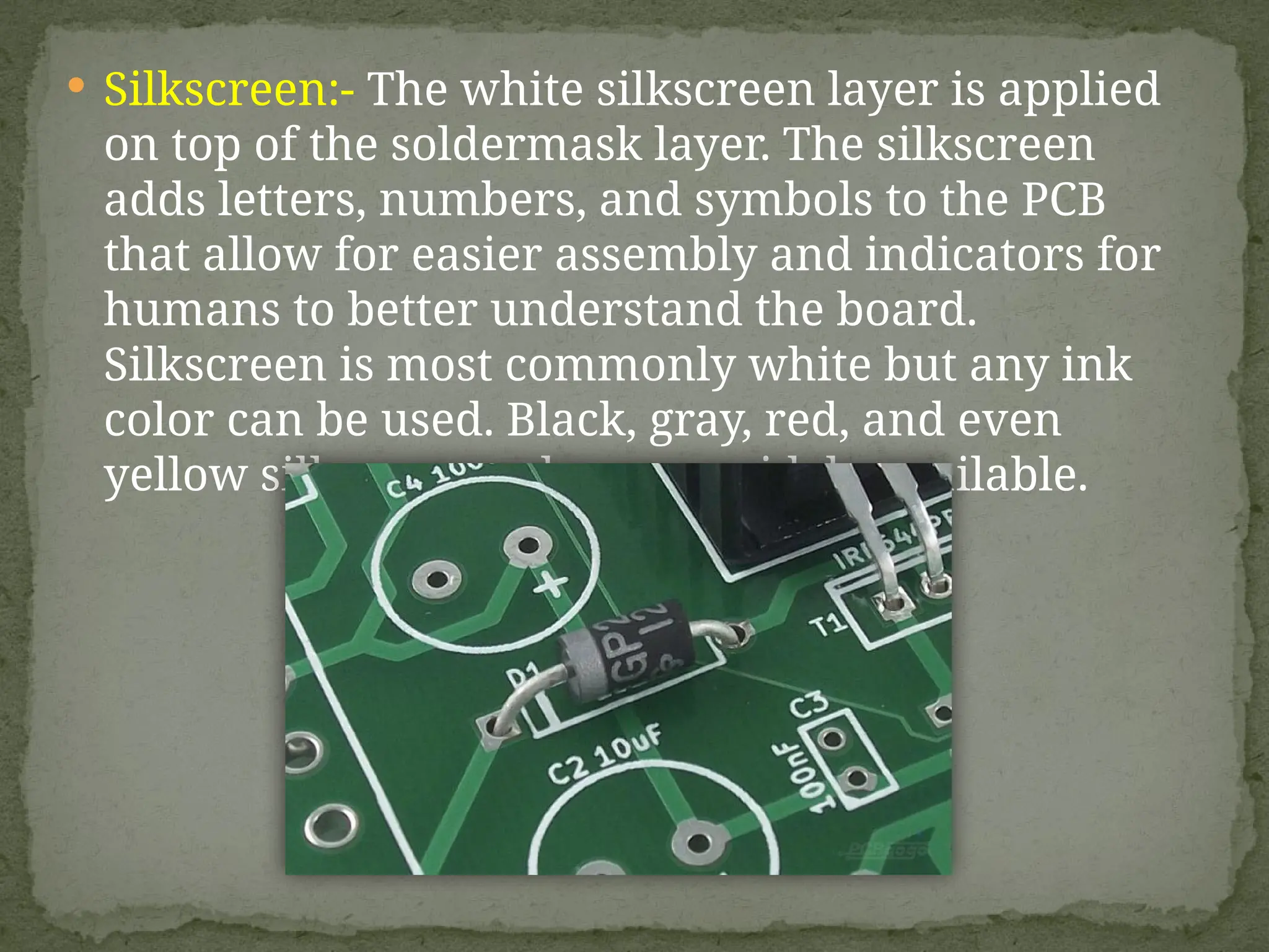
Printed Circuit
Board
PCB
 Introduction to PCB
 Types of PCB
 Composition
 IPC standards
 Manufacturing process Steps
Contents
 PCB stands for printed circuit board, which is a board
with conductive lines etched or printed on a non-
conductive material. It's used to assemble electronic
components and their connections into a single circuit.
 PCB were first developed by an Australian engineer Paul
Eisler.
 PCB are the backbone of electrical devices.
 They can be customized to any specification to users
requirements.
Introduction to PCB
 VIDEO
 Single Sided PCBs
 Double Sided PCBs
 Multi-layer PCBs
 Rigid PCBs
 Flexible PCBs
 Rigid-Flex-PCBs
TYPES OF PCBs
 Single Sided PCB :- Component
placement/Routing only on one
side(TOP/BOTTOM)
 Have one layer of copper foil on one side, and a
substrate layer on the other. These boards are
basic, cost-effective, and easy to repair.
TYPES OF PCBs
 Double Sided PCB :- Component
placement/Routing on both side(TOP&BOTTOM)
 Have copper foil layers on both sides, with a
substrate layer in the middle
TYPES OF PCBs
 Multi-layer PCB :- Component placement on both side
and Routing also internal layers.
 Have multiple copper layers, usually with at least four,
and multiple substrate layers in the middle. The layers
are stacked and bonded together
 Multilayer PCBs are more complex and have higher
component density than single or double-layer
boards. They are used in advanced computers,
communication devices, and high-density integrated
circuits. They are also used in medical devices,
automotive and aerospace components, and industrial
machines.
TYPES OF PCBs
 Rigid PCB:- form of circuit board which are solid and
inflexible in their structure and therefore cannot be
bent or flexed They're made up of several different
layers, such as a substrate layer, a copper layer, a
solder mask layer and a silk screen layer, which are
joined together via adhesive and heat.
 Flexible PCB:- a patterned arrangement of printed
circuitry and components that utilizes flexible base
material with or without flexible cover. Flex PCBs are
made up of a flexible polyimide film substrate and one or
more thin layers of metallic material, usually copper
 Rigid-Flex PCB:- A rigid flex PCB is a printed circuit
board (PCB) that combines flexible and rigid circuit
boards to create a board that can be folded or flexed
 A PCB's layer count is commonly based on its number
of conductive layers. However, a PCB also includes
other types of layers, which are laminated together
in alternating patterns of conductive and insulating
material. Today's PCBs always contain the following
four types of layers:
PCB Composition
 Substrate:- This is the base, or core, layer. It is typically a
rigid insulating material such as FR-4, a fiberglass/epoxy
composite. In some cases, the substrate is a flexible material,
usually plastic, which can fold or bend to accommodate
space requirements. Flexible substrates can also withstand
higher temperatures and other harsh conditions.
 Cheaper PCBs and perf boards will be made with other
materials such as epoxies or phenolics which lack the
durability of FR4 but are much less expensive.
 {FR4 is a standard defined by the NEMA (National Electrical Manufacturers
Association) for a glass-reinforced epoxy resin laminate}
 Conductive:- This layer is usually made from a
thin sheet of copper. On a single-sided (or single-
layer) PCB, there is one conductive layer
laminated to the substrate. On a double-sided (or
double layer) PCB, there are two conductive
layers, one on each side of the substrate. A
multilayer PCB alternates between the substrate
and conductive layers.
 Solder mask:- The conductive layer is covered
with a solder mask, a nonconductive material
that gives PCBs their green color, although other
colors can be used. The solder mask acts as an
insulator for the underlying traces that are
etched in the conductive material.
 Silkscreen:- The white silkscreen layer is applied
on top of the soldermask layer. The silkscreen
adds letters, numbers, and symbols to the PCB
that allow for easier assembly and indicators for
humans to better understand the board.
Silkscreen is most commonly white but any ink
color can be used. Black, gray, red, and even
yellow silkscreen colors are widely available.
 Printed circuit board (PCB) classes are a categorization system that indicates the
quality and reliability of a PCB. The IPC-6011 standard classifies PCBs into three classes,
with Class 1 being the lowest quality and Class 3 being the highest:
 Class 1: Used for general electronics products
 Class 2: Used for devices that require high reliability but not at a critical level
 Class 3: Used for devices that require the highest manufacturing standards, such as
those found in airplanes
 The class of a PCB is determined by the level of inspection and quality standards it
must meet. The appropriate class for a PCB depends on several factors,
including: circuit density, routing complexity, layer count, and electrical performance
needs.
 PCBs can also be classified by other factors, such as: Substrate material, Rigid or
flexible, and Scope of application.
 IPC-2221, IPC-A-600, IPC-A-610, IPC-6012, IPC-A-620, IPC-7351, IPC-2581, IPC-7711/IPC7721, IPC-
2581, IPC-ESD-2020
IPC (Institute for Printed Circuits)
standards
 PCB Schematic Design and generating Gerber: –
2D binary image used to describe the printed
circuit board images copper layer solder mask.
 Drilling holes
 Etching process
 Solder mask coating
 Silkscreen
Manufacturing Process
 VIDEO
THANK YOU
 FR-4 A standard for PCBs that uses FR-4, a
fire resistant material, sandwiched between
two layers of laminated copper
 FR4 is a standard defined by the NEMA (National
Electrical Manufacturers Association) for a glass-
reinforced epoxy resin laminate
FR-4
FR-4 is a common choice for PCB manufacturing
because of its versatility, cost, and performance.
The FR stands for "flame retardant", and the 4
indicates that it's made of woven glass-reinforced
epoxy resin. The epoxy resin in FR-4 contains
bromine and halogen to prevent the spread of fire
and extinguish flames.
FR-4's life span depends on how and where it's
used. It can be a permanent material in equipment
or machinery, but exposure to ultraviolet light can
shorten its life.

printed circuit board PCB basics and standerds

  • 1.
  • 2.
     Introduction toPCB  Types of PCB  Composition  IPC standards  Manufacturing process Steps Contents
  • 3.
     PCB standsfor printed circuit board, which is a board with conductive lines etched or printed on a non- conductive material. It's used to assemble electronic components and their connections into a single circuit.  PCB were first developed by an Australian engineer Paul Eisler.  PCB are the backbone of electrical devices.  They can be customized to any specification to users requirements. Introduction to PCB
  • 4.
  • 5.
     Single SidedPCBs  Double Sided PCBs  Multi-layer PCBs  Rigid PCBs  Flexible PCBs  Rigid-Flex-PCBs TYPES OF PCBs
  • 6.
     Single SidedPCB :- Component placement/Routing only on one side(TOP/BOTTOM)  Have one layer of copper foil on one side, and a substrate layer on the other. These boards are basic, cost-effective, and easy to repair. TYPES OF PCBs
  • 7.
     Double SidedPCB :- Component placement/Routing on both side(TOP&BOTTOM)  Have copper foil layers on both sides, with a substrate layer in the middle TYPES OF PCBs
  • 8.
     Multi-layer PCB:- Component placement on both side and Routing also internal layers.  Have multiple copper layers, usually with at least four, and multiple substrate layers in the middle. The layers are stacked and bonded together  Multilayer PCBs are more complex and have higher component density than single or double-layer boards. They are used in advanced computers, communication devices, and high-density integrated circuits. They are also used in medical devices, automotive and aerospace components, and industrial machines. TYPES OF PCBs
  • 10.
     Rigid PCB:-form of circuit board which are solid and inflexible in their structure and therefore cannot be bent or flexed They're made up of several different layers, such as a substrate layer, a copper layer, a solder mask layer and a silk screen layer, which are joined together via adhesive and heat.  Flexible PCB:- a patterned arrangement of printed circuitry and components that utilizes flexible base material with or without flexible cover. Flex PCBs are made up of a flexible polyimide film substrate and one or more thin layers of metallic material, usually copper  Rigid-Flex PCB:- A rigid flex PCB is a printed circuit board (PCB) that combines flexible and rigid circuit boards to create a board that can be folded or flexed
  • 11.
     A PCB'slayer count is commonly based on its number of conductive layers. However, a PCB also includes other types of layers, which are laminated together in alternating patterns of conductive and insulating material. Today's PCBs always contain the following four types of layers: PCB Composition
  • 12.
     Substrate:- Thisis the base, or core, layer. It is typically a rigid insulating material such as FR-4, a fiberglass/epoxy composite. In some cases, the substrate is a flexible material, usually plastic, which can fold or bend to accommodate space requirements. Flexible substrates can also withstand higher temperatures and other harsh conditions.  Cheaper PCBs and perf boards will be made with other materials such as epoxies or phenolics which lack the durability of FR4 but are much less expensive.  {FR4 is a standard defined by the NEMA (National Electrical Manufacturers Association) for a glass-reinforced epoxy resin laminate}
  • 13.
     Conductive:- Thislayer is usually made from a thin sheet of copper. On a single-sided (or single- layer) PCB, there is one conductive layer laminated to the substrate. On a double-sided (or double layer) PCB, there are two conductive layers, one on each side of the substrate. A multilayer PCB alternates between the substrate and conductive layers.
  • 14.
     Solder mask:-The conductive layer is covered with a solder mask, a nonconductive material that gives PCBs their green color, although other colors can be used. The solder mask acts as an insulator for the underlying traces that are etched in the conductive material.
  • 15.
     Silkscreen:- Thewhite silkscreen layer is applied on top of the soldermask layer. The silkscreen adds letters, numbers, and symbols to the PCB that allow for easier assembly and indicators for humans to better understand the board. Silkscreen is most commonly white but any ink color can be used. Black, gray, red, and even yellow silkscreen colors are widely available.
  • 16.
     Printed circuitboard (PCB) classes are a categorization system that indicates the quality and reliability of a PCB. The IPC-6011 standard classifies PCBs into three classes, with Class 1 being the lowest quality and Class 3 being the highest:  Class 1: Used for general electronics products  Class 2: Used for devices that require high reliability but not at a critical level  Class 3: Used for devices that require the highest manufacturing standards, such as those found in airplanes  The class of a PCB is determined by the level of inspection and quality standards it must meet. The appropriate class for a PCB depends on several factors, including: circuit density, routing complexity, layer count, and electrical performance needs.  PCBs can also be classified by other factors, such as: Substrate material, Rigid or flexible, and Scope of application.  IPC-2221, IPC-A-600, IPC-A-610, IPC-6012, IPC-A-620, IPC-7351, IPC-2581, IPC-7711/IPC7721, IPC- 2581, IPC-ESD-2020 IPC (Institute for Printed Circuits) standards
  • 17.
     PCB SchematicDesign and generating Gerber: – 2D binary image used to describe the printed circuit board images copper layer solder mask.  Drilling holes  Etching process  Solder mask coating  Silkscreen Manufacturing Process
  • 18.
  • 19.
  • 20.
     FR-4 Astandard for PCBs that uses FR-4, a fire resistant material, sandwiched between two layers of laminated copper  FR4 is a standard defined by the NEMA (National Electrical Manufacturers Association) for a glass- reinforced epoxy resin laminate FR-4
  • 21.
    FR-4 is acommon choice for PCB manufacturing because of its versatility, cost, and performance. The FR stands for "flame retardant", and the 4 indicates that it's made of woven glass-reinforced epoxy resin. The epoxy resin in FR-4 contains bromine and halogen to prevent the spread of fire and extinguish flames. FR-4's life span depends on how and where it's used. It can be a permanent material in equipment or machinery, but exposure to ultraviolet light can shorten its life.