The document summarizes the High Electron Mobility Transistor (HEMT), a type of field effect transistor used for applications requiring low noise and high performance at microwave frequencies. HEMTs utilize a hetero-junction consisting of different materials on either side of a PN junction. Common materials are Aluminum Gallium Arsenide and Gallium Arsenide. HEMTs offer advantages like high gain, switching speed, and efficiency for applications from 5-100 GHz, including telecommunications, radar, and other RF designs.


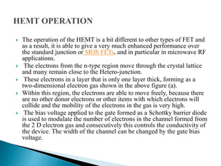


![Mimo [new]](https://cdn.slidesharecdn.com/ss_thumbnails/mimonew-150914045107-lva1-app6892-thumbnail.jpg?width=640&height=640&fit=bounds)


