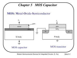
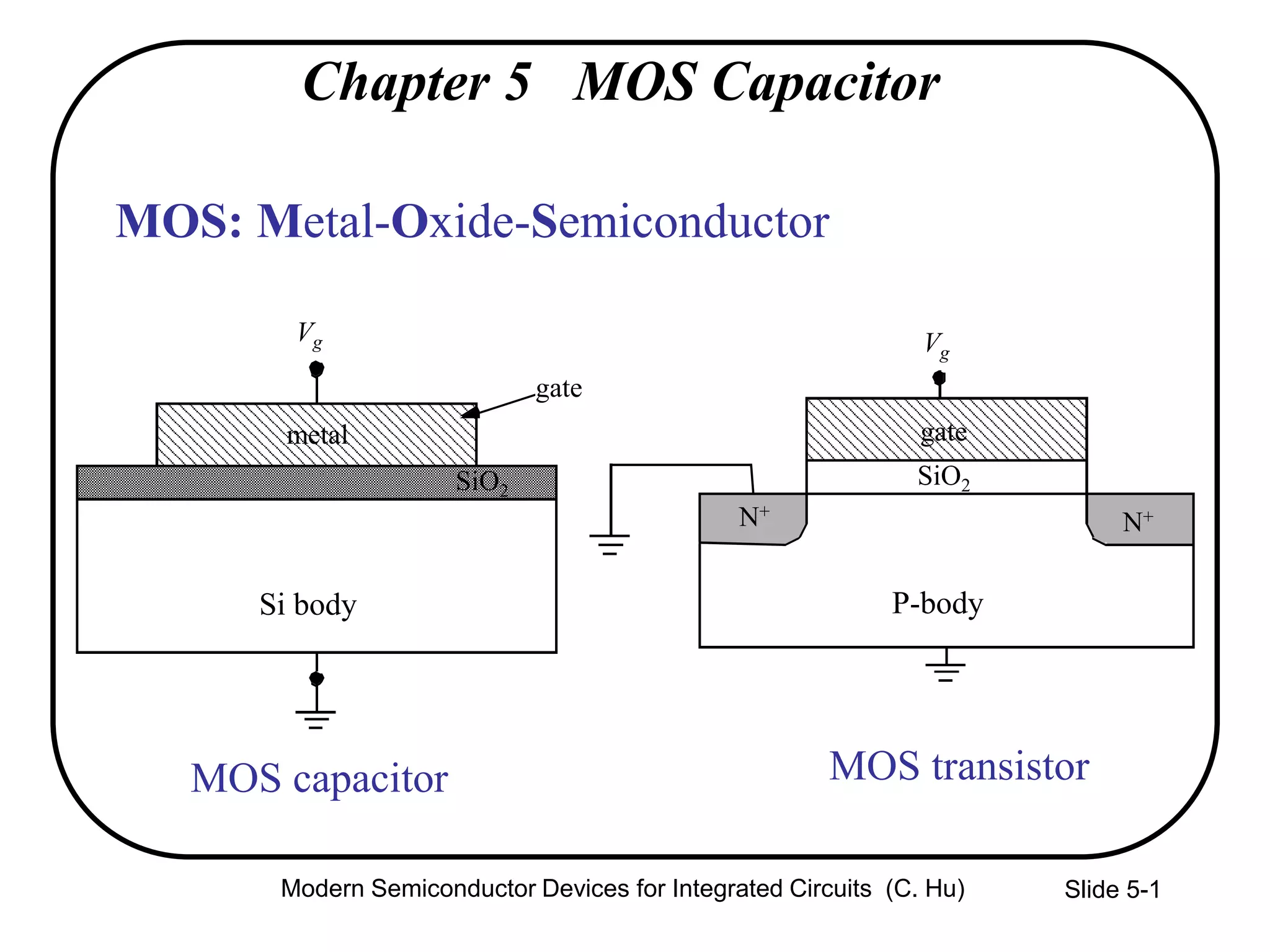
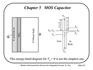
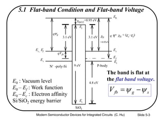
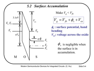
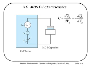
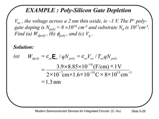
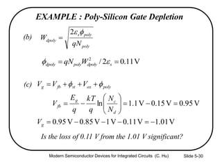
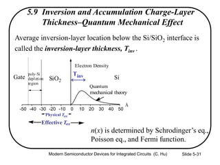
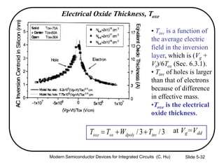
This document summarizes key concepts about MOS capacitors including:
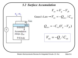
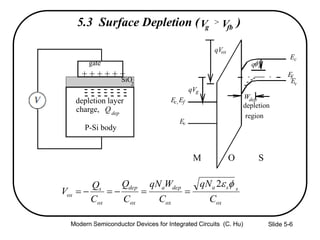
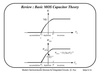
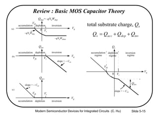
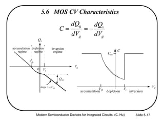
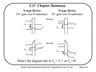
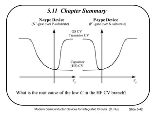
1) The structure and operation of an MOS capacitor including accumulation, depletion, and inversion regions depending on the gate voltage Vg relative to the flat-band voltage Vfb and threshold voltage Vt.
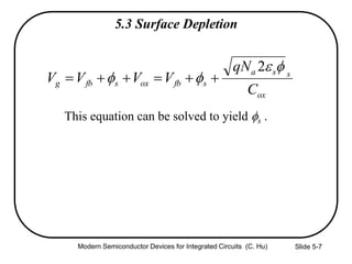
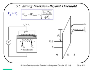
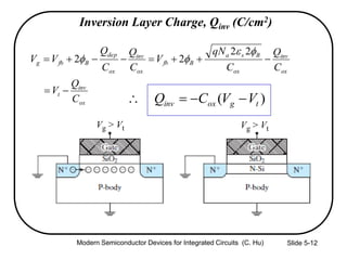
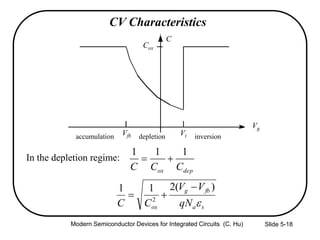
2) Equations relating surface potential φs, depletion width Wdep, oxide capacitance Cox, and inversion charge Qinv to the applied gate voltage Vg.
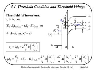
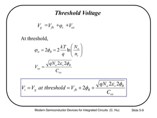
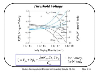
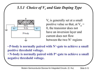
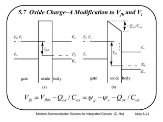
3) Sources of threshold voltage Vt variation including body doping, oxide thickness Tox, and fixed oxide charge Qox.
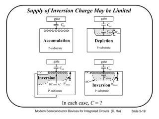
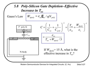
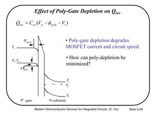
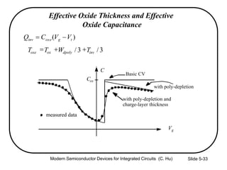
4) Effects of poly-silicon gate depletion on the effective oxide thickness and inversion charge Qinv.


![Agilent ADS 模擬手冊 [實習3] 壓控振盪器模擬](https://cdn.slidesharecdn.com/ss_thumbnails/3adsosc-150613072819-lva1-app6892-thumbnail.jpg?width=640&height=640&fit=bounds)