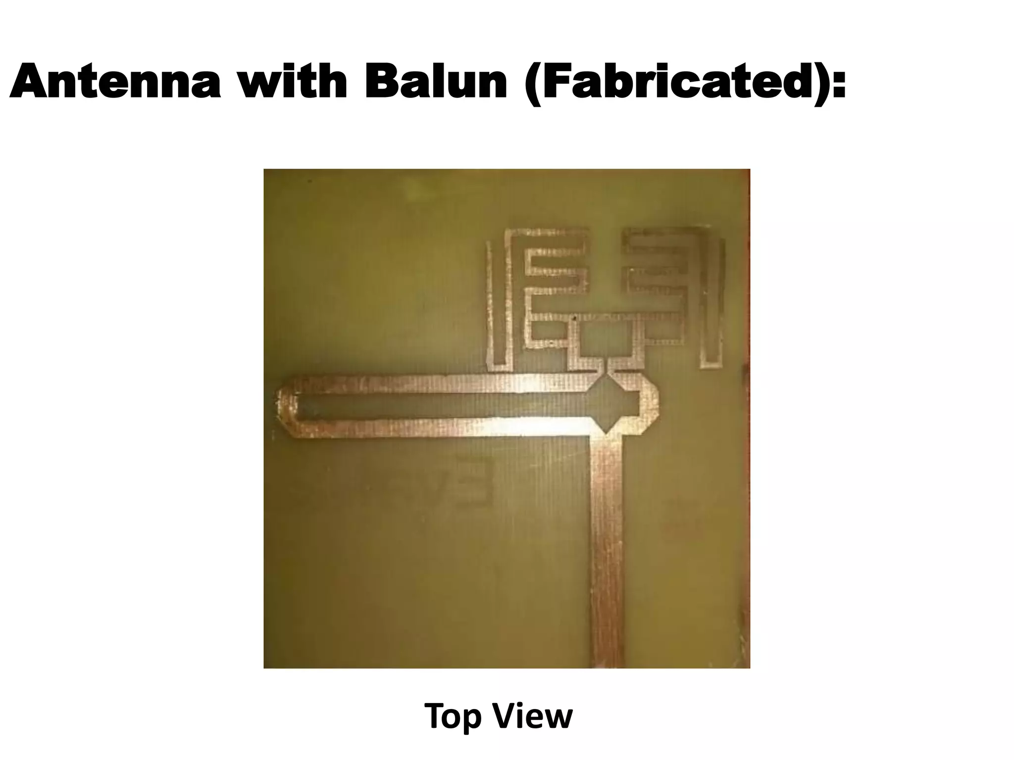
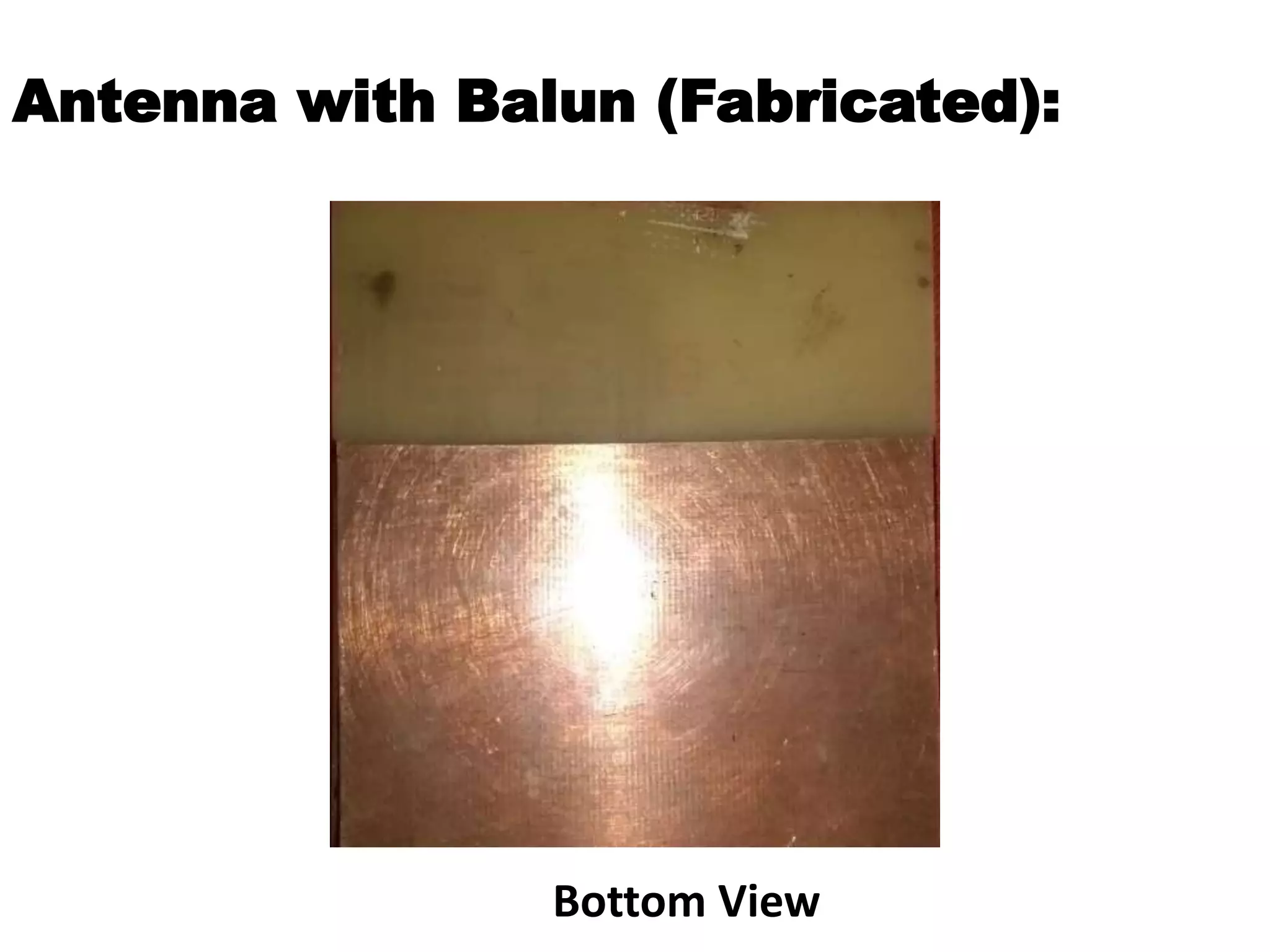
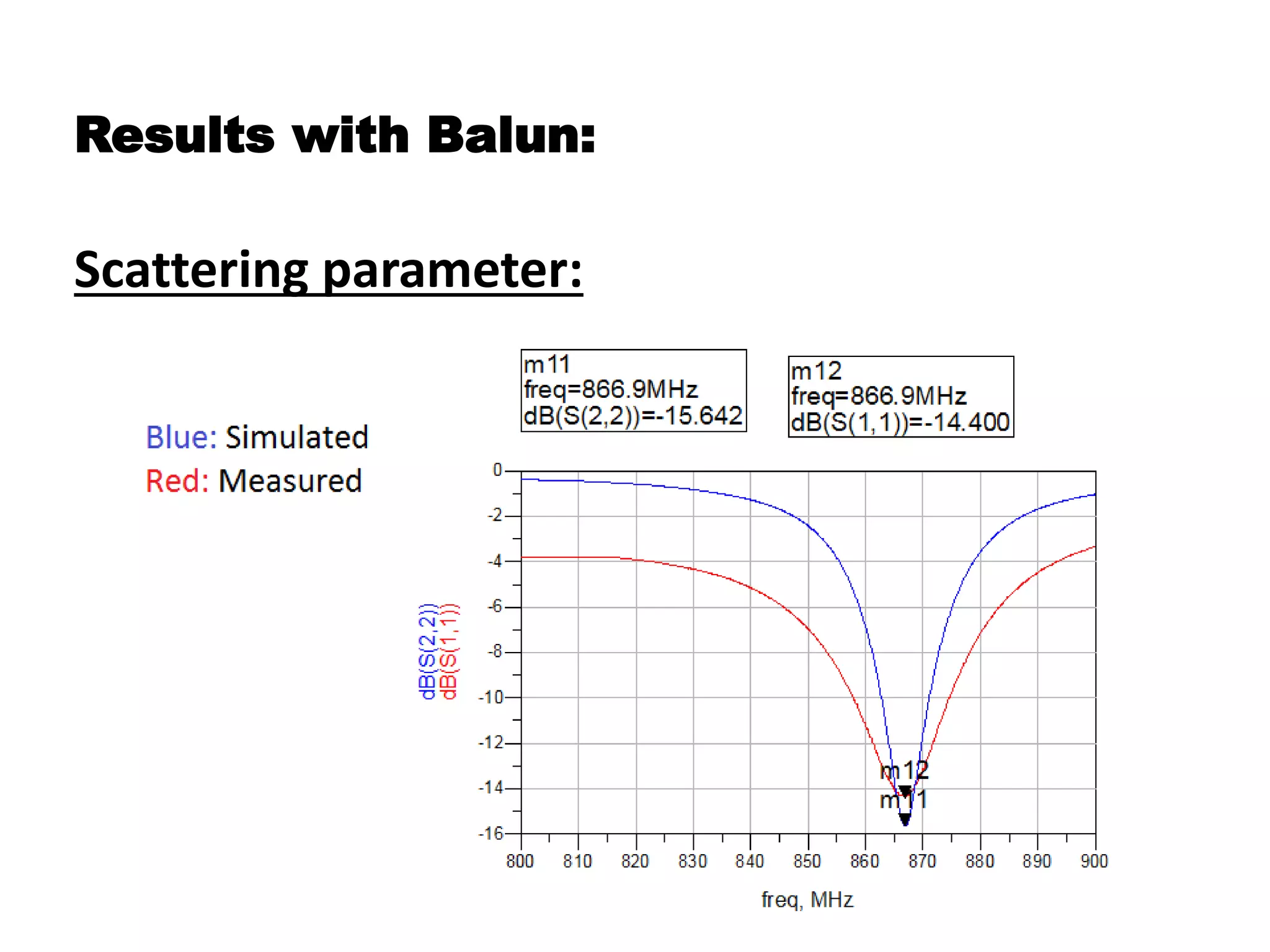
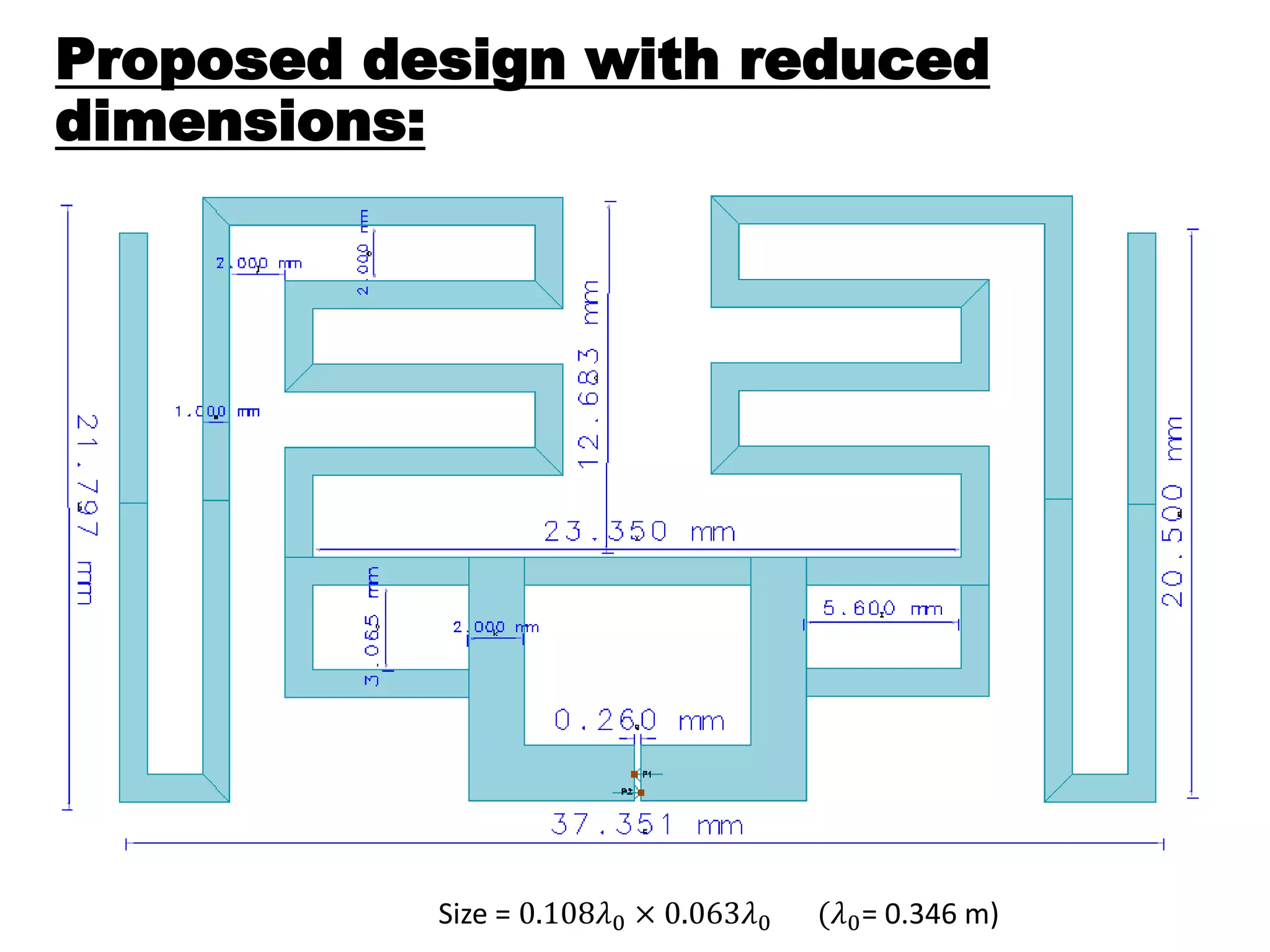
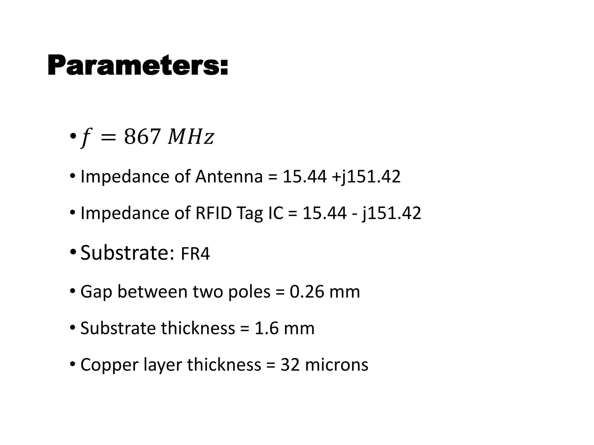
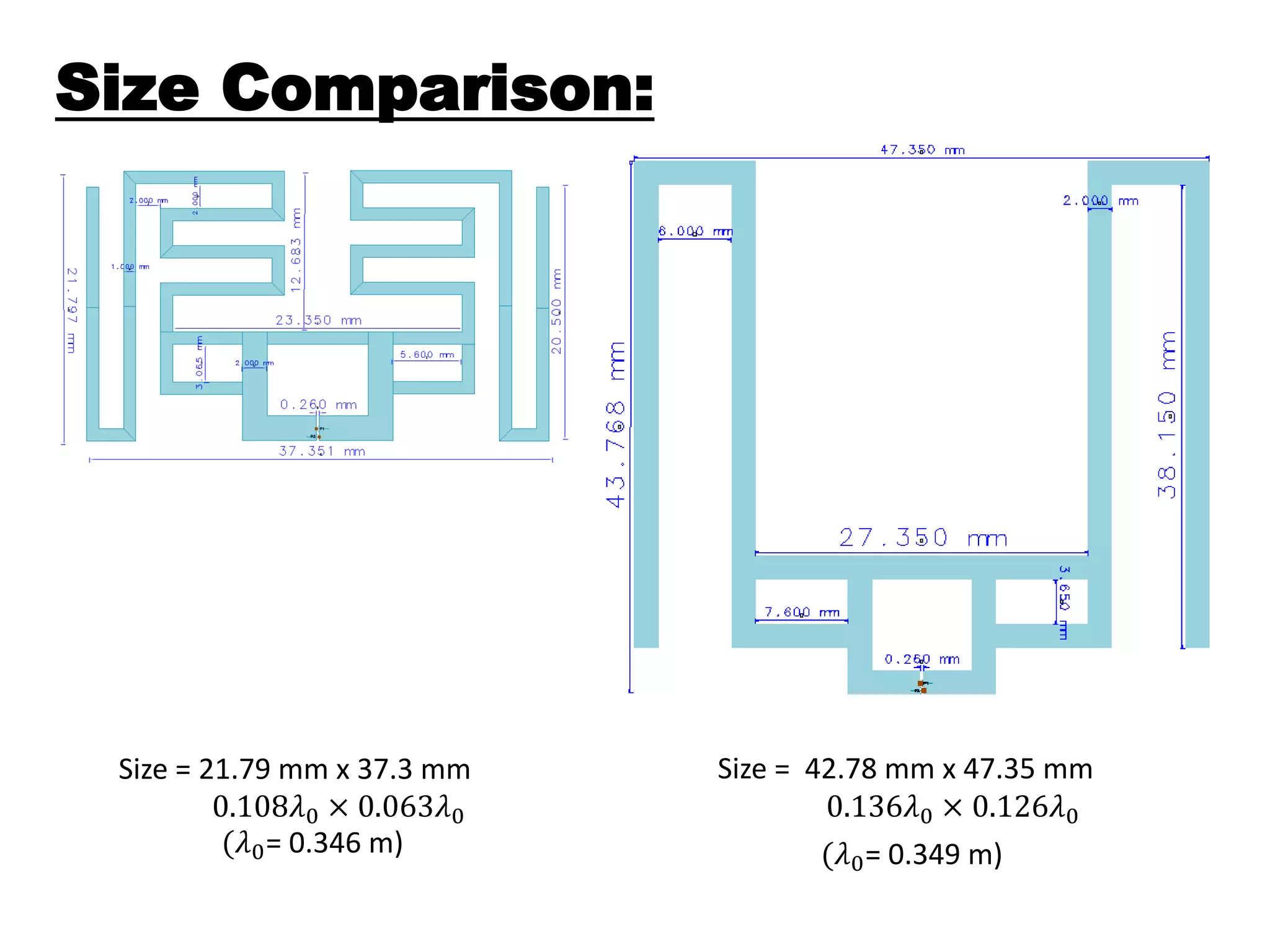
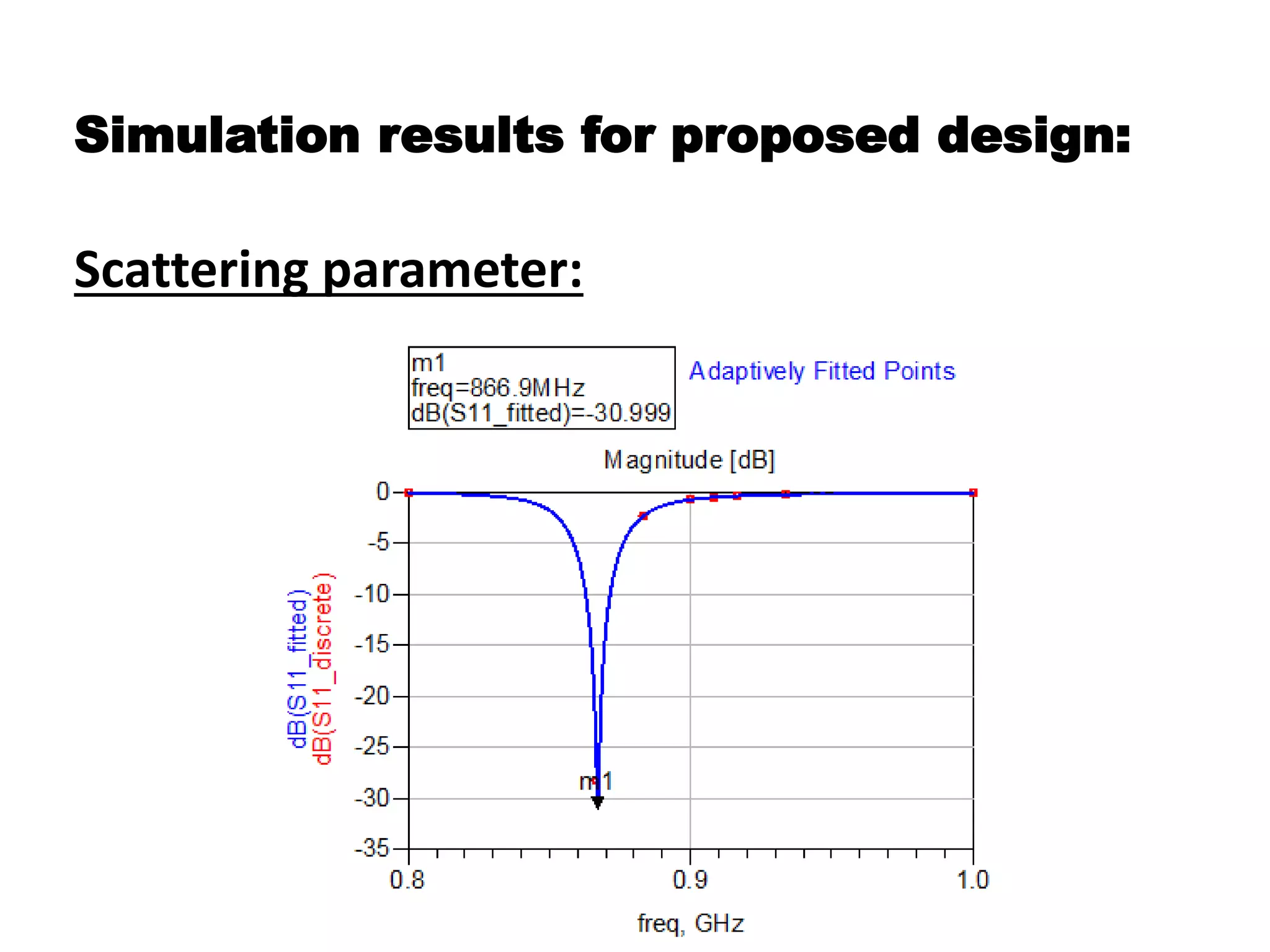
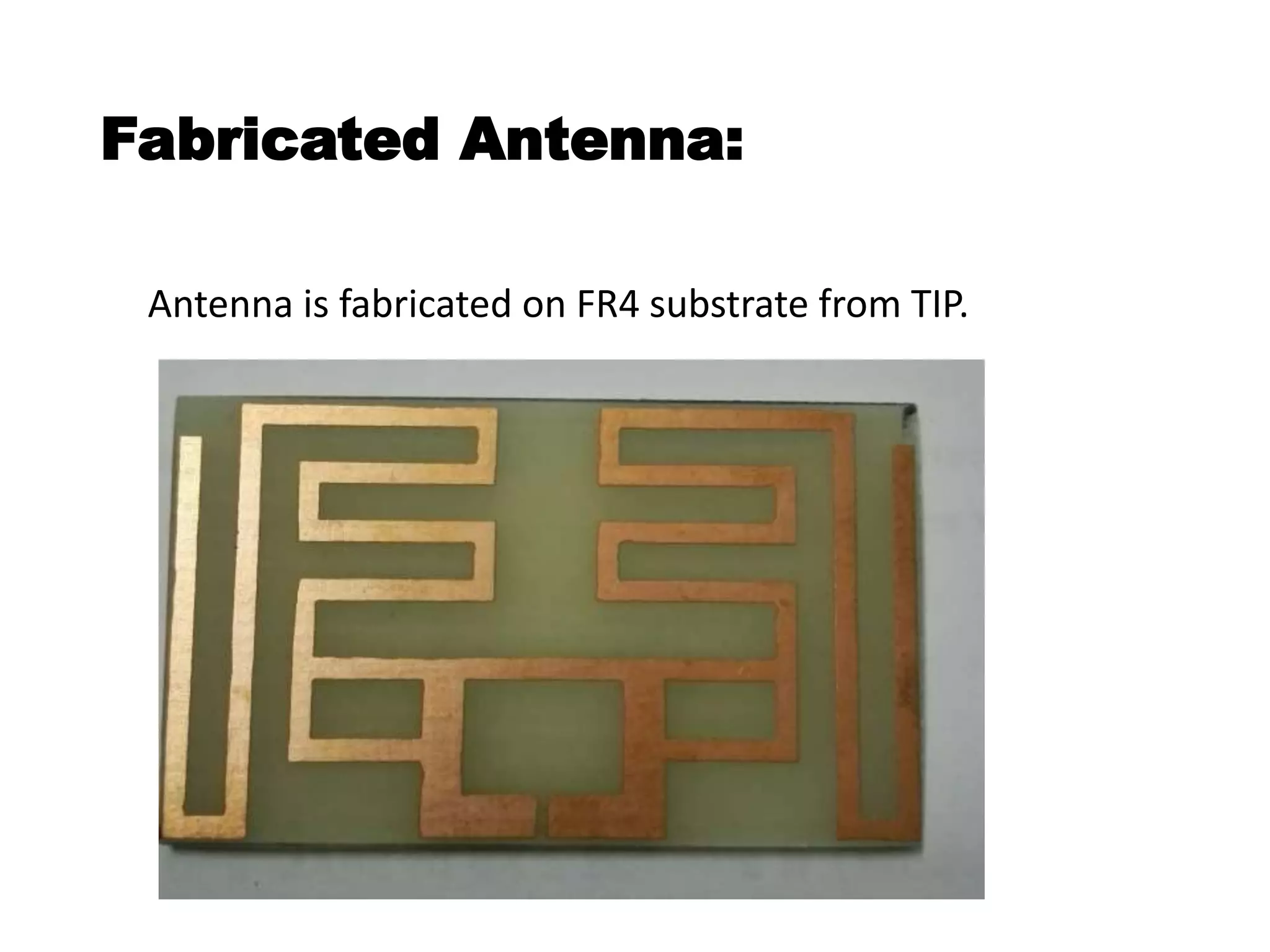
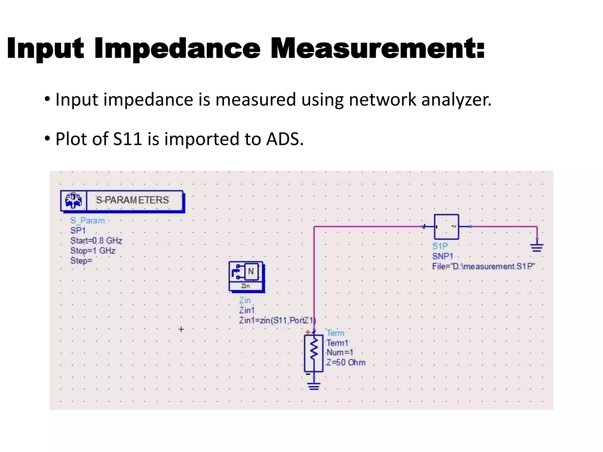
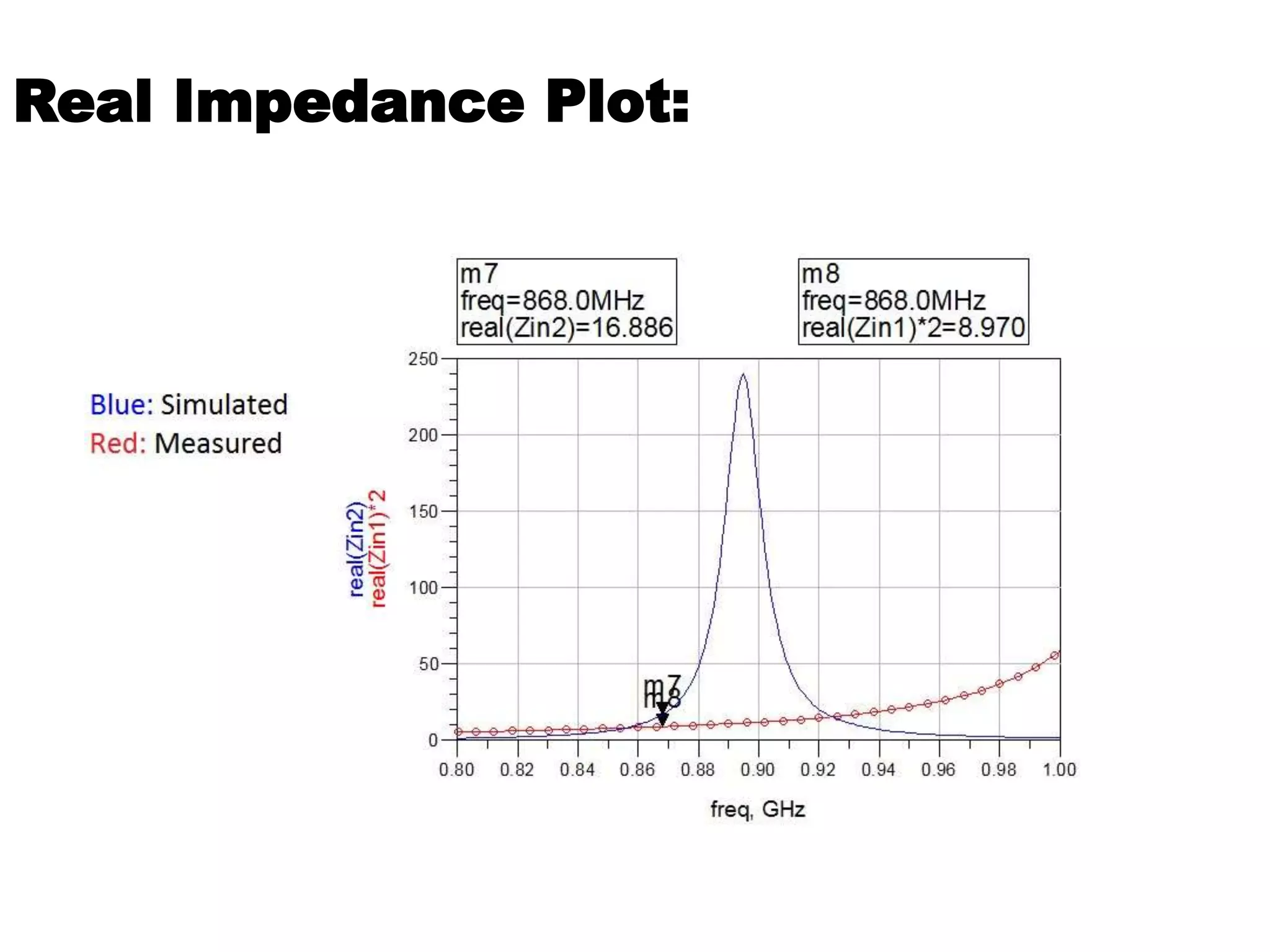
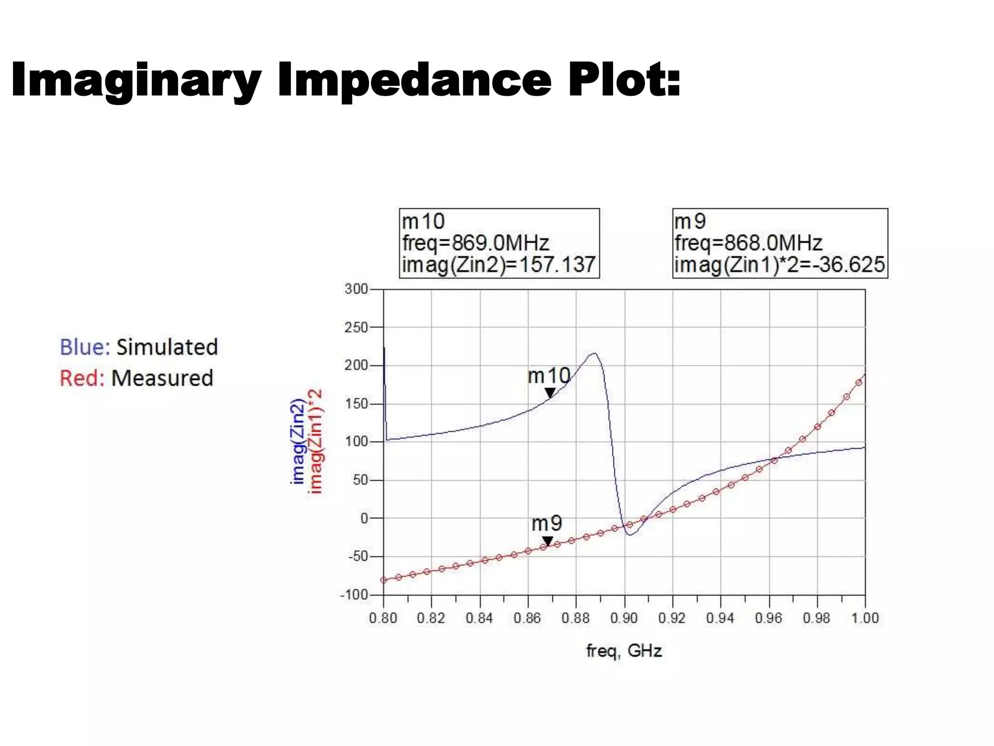
This document describes the design, simulation, and fabrication of a passive UHF RFID tag. The objectives are to design, simulate, and fabricate a passive UHF RFID tag and measure its input impedance. The project involves studying existing RFID tag designs, optimizing a design for implementation on an FR4 substrate, fabricating the tag, and measuring its input impedance. A proposed tag design is presented with reduced dimensions from an initial design. The tag is fabricated and its input impedance is measured. Additional measurements are taken after adding a microstrip balun to improve impedance matching.
![Block Diagram:
[1] Antenna Theory and Design by Warren L. Stutzman 3rd Edition
Fig.1 Block Diagram of RFID System [1]
Passive RFID Tag System:
• Reader
• Emits RF signal.
• Collects Data stored in tag.
• Tag
• Converts RF signal to DC voltage
for powering up the circuitry.
• Process and returns RF signal
containing identification data.
Introduction:
RFID:
A radio frequency identification (RFID) system identifies an
object without direct contact through digital wireless
techniques.](https://image.slidesharecdn.com/03a2ba57-9853-4f6c-9680-fad2f7f1dd70-150821133552-lva1-app6891/75/FYP-4th-presentation-4-2048.jpg)
![RFID Allocated Freq. Bands [2]:
Frequency Band Name Frequencies Passive Read Distance
Low Frequency (LF) 120-140 KHz 10-120 cm
High Frequency (HF) 13.56 MHz 10-20 cm
Ultra High Frequency (UHF) 865-928 MHz Less than 10 m
Microwave (MW) 2.45 & 5.8 MHz Less than 3 m
Ultra Wideband 3.1-10.6 GHz 10 m
[2] Antenna Theory and Design by Warren L. Stutzman 3rd Edition](https://image.slidesharecdn.com/03a2ba57-9853-4f6c-9680-fad2f7f1dd70-150821133552-lva1-app6891/75/FYP-4th-presentation-5-2048.jpg)
![RFID Frequency Bands [3]
• USA: 902 – 928 MHz
• China : 840.5 – 844.75 / 920.25 – 924.75 MHz
• Europe : 865- 868 MHz
[3] D. Puente, et al “Matching radio frequency identification tag compact dipole
antennas to an arbitrary chip impedance” IET Microwaves, Antennas & Propagation
2008](https://image.slidesharecdn.com/03a2ba57-9853-4f6c-9680-fad2f7f1dd70-150821133552-lva1-app6891/75/FYP-4th-presentation-6-2048.jpg)
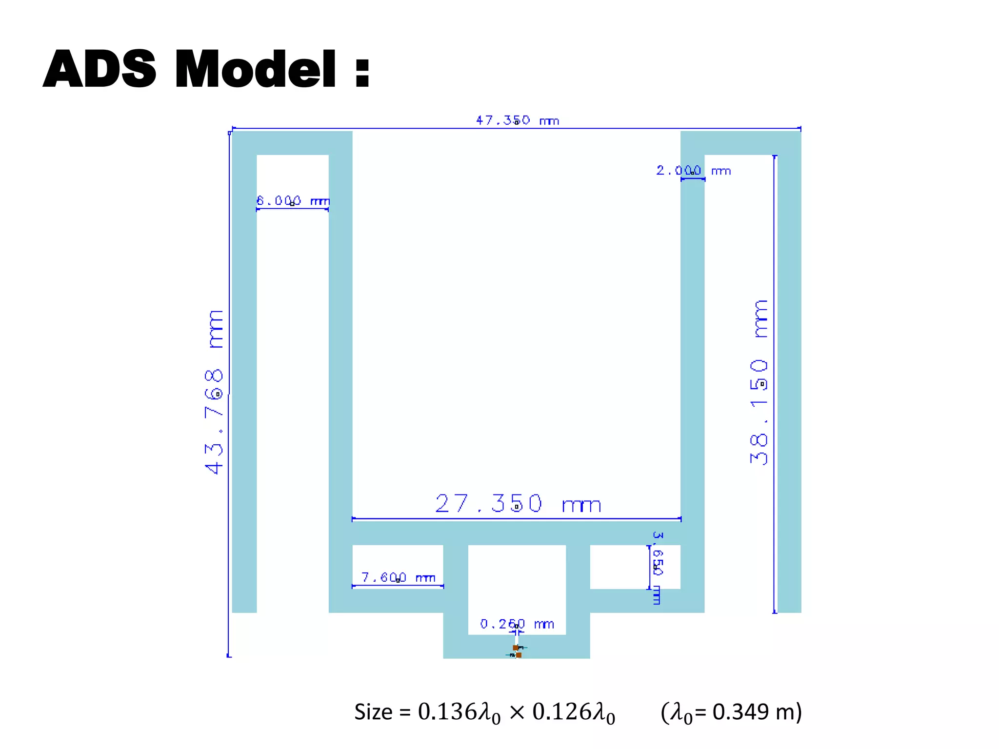
![Physical Structure:
.
Fig. 2. Dimension of the Antenna; a= 2 mm, b = 27.35 mm, c = 32.35 mm,
d = 38 mm, e = 7.6 mm, f = 3.65 mm, g = 6 mm [4]
[4] S. Sajal et al, “A Low Cost Flexible Passive UHF RFID Tag for Sensing Moisture Based on Antenna
Polarization”, IEEE, 2014](https://image.slidesharecdn.com/03a2ba57-9853-4f6c-9680-fad2f7f1dd70-150821133552-lva1-app6891/75/FYP-4th-presentation-8-2048.jpg)
![Size Reduction and Impedance
Matching(Smith Chart)[5] :
For an antenna to have an admittance of 𝑌𝑎 = 𝑔 𝑎 + 𝑗𝑏 𝑎 and the chip
admittance to be 𝑌𝑐 = 𝑔𝑐 + 𝑗𝑏𝑐 for the optimal power transfer
between the antenna and tag 𝑌𝑎 = 𝑌𝑐
∗ at the design frequency
1) Making 𝑔 𝑎 = 𝑔𝑐 by scaling
For 𝑔 𝑎 = 𝑔𝑐 scaling factor is used
𝞺 =
𝑓
𝑓0
Where f is either
𝑓 = 𝑓1
Or 𝑓 = 𝑓2
If 𝑓1 < 𝑓2 𝑠𝑜 𝑓1 is chosen for more compact design.
[5] D. Puente, et al “Matching radio frequency identification tag compact dipole
antennas to an arbitrary chip impedance” IET Microwaves, Antennas & Propagation
2008](https://image.slidesharecdn.com/03a2ba57-9853-4f6c-9680-fad2f7f1dd70-150821133552-lva1-app6891/75/FYP-4th-presentation-13-2048.jpg)
![Size Reduction and Impedance
Matching(Smith Chart)[5] :
2) Making 𝑏 𝑎 = −𝑏𝑐 by short circuit stub.
To make 𝑏 𝑎 = −𝑏 𝑐 we select the proper value of Reactance.
𝑋𝑠𝑡𝑢𝑏 =
1
𝑏 𝑐+𝑏
𝑙 =
1
𝛽
𝑎𝑟𝑐𝑡𝑎𝑛
𝑋𝑠𝑡𝑢𝑏
𝑍0
𝑍0 = 𝜂0 𝐴
𝑍0 Characteristic impedance (for c = 1.2 mm and b = 1.5 mm ,
𝑍0 =226.5)
𝜂0 Intrinsic Impedance (377 Ohm)
[5] D. Puente, et al “Matching radio frequency identification tag compact dipole antennas to
an arbitrary chip impedance” IET Microwaves, Antennas & Propagation 2008](https://image.slidesharecdn.com/03a2ba57-9853-4f6c-9680-fad2f7f1dd70-150821133552-lva1-app6891/75/FYP-4th-presentation-14-2048.jpg)
![Size Reduction and Impedance
Matching(Smith Chart)[5] :
• 𝐴 =
2𝜋
ln(2( 1+𝐾 𝑎 + 4𝐾 𝑎
1 4/ 1+𝐾 𝑎 − 4𝐾 𝑎
1 4))
• 0 ≤ 𝐴 ≤ 1 , 0 ≤ 𝑘 ≤
1
2
• 𝑘 𝑎 = 1 − 𝑘2 , 𝑘 =
𝑐
𝑐+2𝑏
[5] D. Puente, et al “Matching radio frequency identification tag compact dipole antennas to
an arbitrary chip impedance” IET Microwaves, Antennas & Propagation 2008](https://image.slidesharecdn.com/03a2ba57-9853-4f6c-9680-fad2f7f1dd70-150821133552-lva1-app6891/75/FYP-4th-presentation-15-2048.jpg)

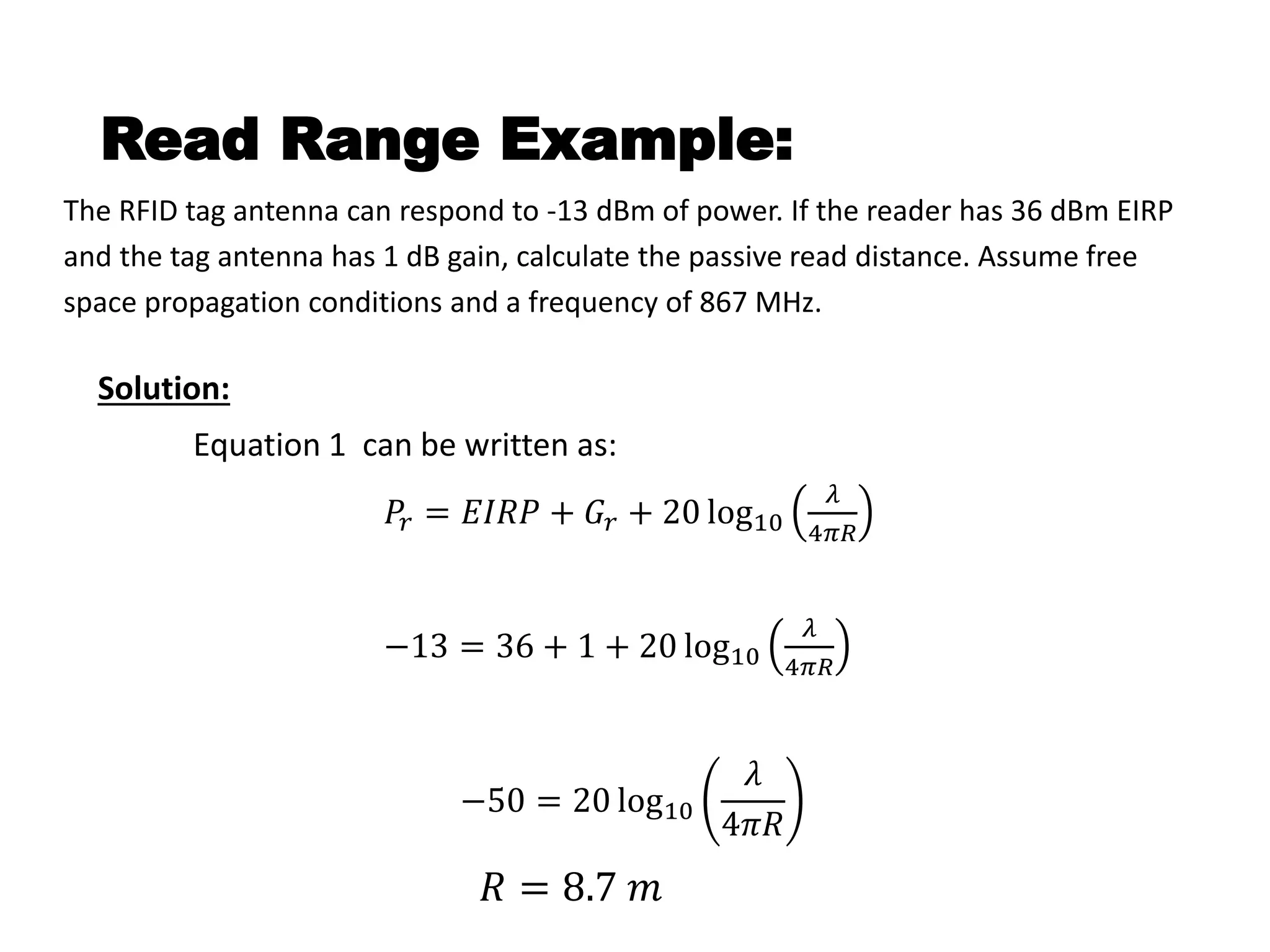
![Read Range Calculation: [6]
Friis Transmission Equation
𝑃𝑟
𝑃𝑡
=
𝜆
4𝜋𝑅
2
𝐺𝑡 𝐺𝑟 (1)
Where R is our read range.
[6] Antenna Theory Analysis and Design by Constantine A. Balanis 3rd Edition](https://image.slidesharecdn.com/03a2ba57-9853-4f6c-9680-fad2f7f1dd70-150821133552-lva1-app6891/75/FYP-4th-presentation-25-2048.jpg)

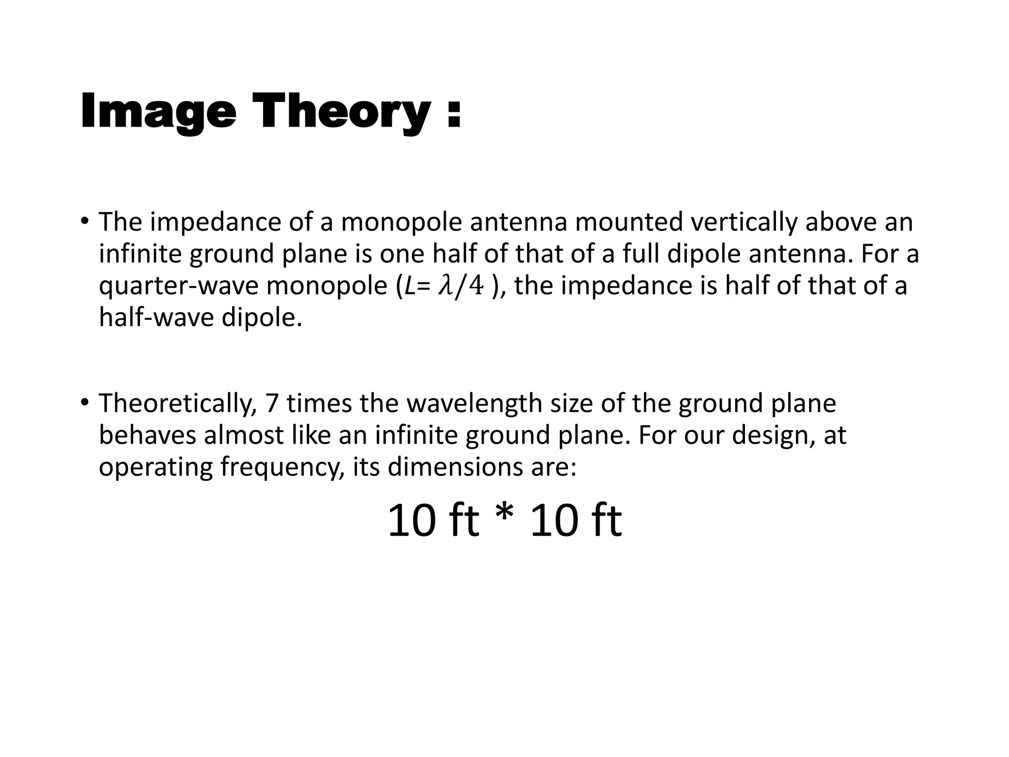
![Image Theory [7]:
The monopole antenna results from applying image theory to the
dipole. If a conducting plane is placed below a single element of length
L/2 carrying a current, then the combined system acts essentially
identically to a dipole of length L except that the radiation takes place
only in the space above the plane, so the directivity is doubled and the
radiation resistance is halved(Figure 3).
Figure 3. Image theory applied to the monopole antenna
[7] ANTENNAS AND PROPAGATION FOR WIRELESS COMMUNICATION SYSTEMS
2nd Edition by SIMON R. SAUNDERS](https://image.slidesharecdn.com/03a2ba57-9853-4f6c-9680-fad2f7f1dd70-150821133552-lva1-app6891/75/FYP-4th-presentation-29-2048.jpg)

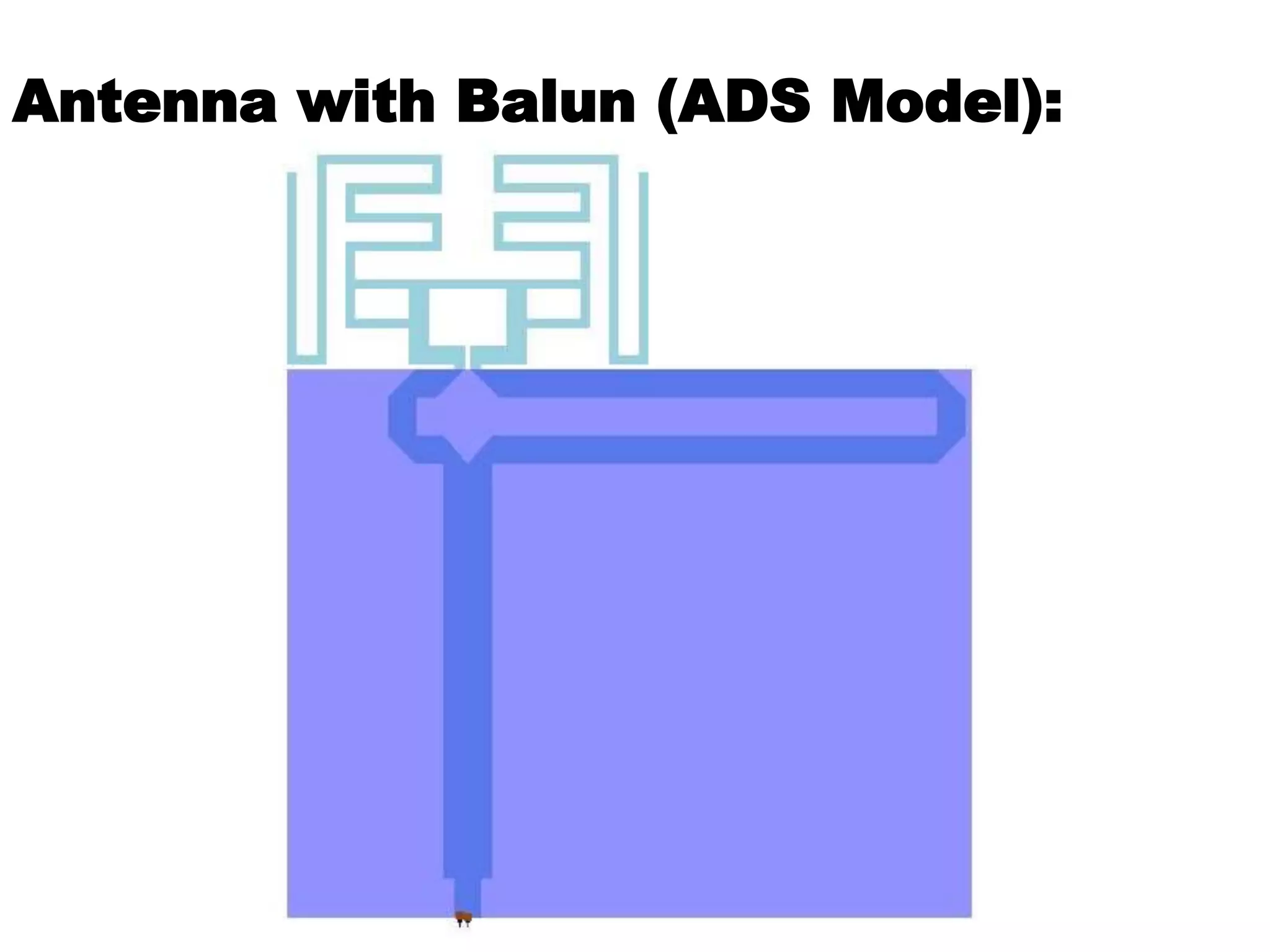
![Designing a Microstrip Balun [8]:
Fig.4 Microstrip Balun
[8] A Broadband unipolar Microstrip to CPS Transition 1997 Asia Pacific Microwave Conference
By changing l1 and l2 so that,
l1-l2= 𝜆 𝑔/4 it gives the
required results .](https://image.slidesharecdn.com/03a2ba57-9853-4f6c-9680-fad2f7f1dd70-150821133552-lva1-app6891/75/FYP-4th-presentation-38-2048.jpg)