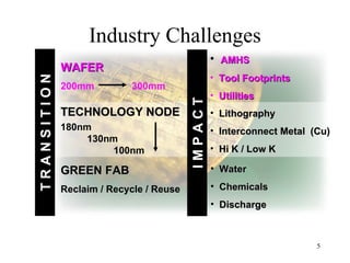
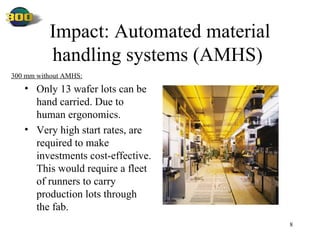
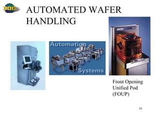
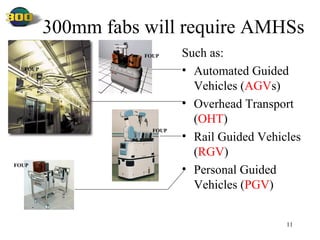
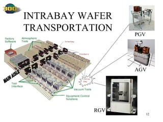
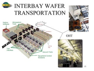
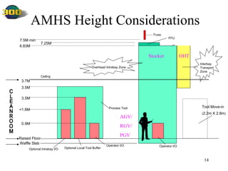
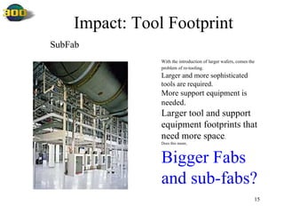
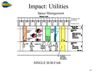
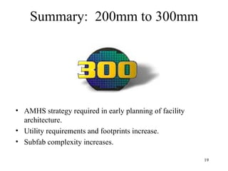
Moving from 200mm to 300mm Microelectronics
T he history of fab development has predominantly centered upon a single model: a clean environment in which gowned personnel carry small containers of wafers from one process tool to another. As wafers got bigger, fabs got  cleaner .
Moore’s Law “ The amount of information storable on a given amount of silicon doubles every year.” Moore’s Law by Gordon Moore, 1964, founded Intel Technology since 1970   # of transistors per chip  memory size Geometric features Technology since 1970   # of transistors per chip  memory size Geometric features The Need for Speed increased exponentially decreased 1/2 every 18 months
The primary driver for producing chips on 300 mm wafers is economics: Reducing cost by creating  more chips per wafer 300-mm wafers have 125% more silicon surface area The net gain in chip count from 300-mm wafers can be as high as 160%  200mm
Industry Challenges AMHS Tool Footprints Utilities TECHNOLOGY NODE 180nm 130nm 100nm Lithography  Interconnect Metal  (Cu) Hi K / Low K GREEN FAB Reclaim / Recycle / Reuse Water Chemicals Discharge T R A N S I T I O N I M P A C T WAFER 200mm  300mm
In the early 1980s, two different concepts of fab functioning emerged:   Minienvironments  Automated material handling systems (AMHS)
Minienvironments Provide solutions for: Product Quality  Improvement by Contamination reduction Therefore risk of contamination, scratches, misprocessing, scrap and rework should be minimized.  This is done through computer integrated manufacturing (CIM), standard mechanical interfaces (SMIF),  minienvironments  and AMHSs 300mm wafers are expensive, 10x more then 200mm
Impact: Automated material handling systems (AMHS)   Only 13 wafer lots can be hand carried. Due to human ergonomics. Very high start rates, are required to make investments cost-effective. This would require a fleet of runners to carry production lots through the fab. 300 mm without AMHS:
In a clean environment  People = Particles
AUTOMATED WAFER HANDLING Front Opening Unified Pod (FOUP)
300mm fabs will require AMHSs Such as: Automated Guided Vehicles ( AGV s) Overhead Transport ( OHT ) Rail Guided Vehicles ( RGV ) Personal Guided Vehicles ( PGV ) FOUP FOUP FOUP FOUP
INTRABAY WAFER TRANSPORTATION MAIN AISLE AGV PGV RGV
INTERBAY WAFER TRANSPORTATION MAIN AISLE OHT
AMHS Height Considerations CLEANROOM Stocker OHT AGV/ RGV/ PGV Interbay Transport Zone Overhead Intrabay Zone Process Tool Ceiling Raised Floor 6.83M  3.5M 3.5M <1.8M 0.9M 3.7M Stocker Tool Move-in ( 2.2m X 2.8m ) Operator I/O Operator I/O Optional Local Tool Buffer Optional Intrabay I/O FFU Truss 7.5M min 7.25M Waffle Slab
SubFab With the introduction of larger wafers, comes the problem of re-tooling . Larger and more sophisticated tools are required. More support equipment is needed. Larger tool and support equipment footprints that need more space . Does this mean; Bigger Fabs and sub-fabs? Impact: Tool Footprint
Space Management WAFFLE SLAB RAISED ACCESS FLOORING SINGLE SUB-FAB Impact: Utilities
Space Management DOUBLE SUB-FAB WAFFLE SLAB RAISED ACCESS FLOORING
SPACE MANAGEMENT   BUILDING SECTION
Summary:  200mm to 300mm AMHS strategy required in early planning of facility architecture. Utility requirements and footprints increase. Subfab complexity increases.

From 200 to 300 MM Fabs

  • 1.
    Moving from 200mmto 300mm Microelectronics
  • 2.
    T he historyof fab development has predominantly centered upon a single model: a clean environment in which gowned personnel carry small containers of wafers from one process tool to another. As wafers got bigger, fabs got cleaner .
  • 3.
    Moore’s Law “The amount of information storable on a given amount of silicon doubles every year.” Moore’s Law by Gordon Moore, 1964, founded Intel Technology since 1970 # of transistors per chip memory size Geometric features Technology since 1970 # of transistors per chip memory size Geometric features The Need for Speed increased exponentially decreased 1/2 every 18 months
  • 4.
    The primary driverfor producing chips on 300 mm wafers is economics: Reducing cost by creating more chips per wafer 300-mm wafers have 125% more silicon surface area The net gain in chip count from 300-mm wafers can be as high as 160% 200mm
  • 5.
    Industry Challenges AMHSTool Footprints Utilities TECHNOLOGY NODE 180nm 130nm 100nm Lithography Interconnect Metal (Cu) Hi K / Low K GREEN FAB Reclaim / Recycle / Reuse Water Chemicals Discharge T R A N S I T I O N I M P A C T WAFER 200mm 300mm
  • 6.
    In the early1980s, two different concepts of fab functioning emerged: Minienvironments Automated material handling systems (AMHS)
  • 7.
    Minienvironments Provide solutionsfor: Product Quality Improvement by Contamination reduction Therefore risk of contamination, scratches, misprocessing, scrap and rework should be minimized. This is done through computer integrated manufacturing (CIM), standard mechanical interfaces (SMIF), minienvironments and AMHSs 300mm wafers are expensive, 10x more then 200mm
  • 8.
    Impact: Automated materialhandling systems (AMHS) Only 13 wafer lots can be hand carried. Due to human ergonomics. Very high start rates, are required to make investments cost-effective. This would require a fleet of runners to carry production lots through the fab. 300 mm without AMHS:
  • 9.
    In a cleanenvironment People = Particles
  • 10.
    AUTOMATED WAFER HANDLINGFront Opening Unified Pod (FOUP)
  • 11.
    300mm fabs willrequire AMHSs Such as: Automated Guided Vehicles ( AGV s) Overhead Transport ( OHT ) Rail Guided Vehicles ( RGV ) Personal Guided Vehicles ( PGV ) FOUP FOUP FOUP FOUP
  • 12.
    INTRABAY WAFER TRANSPORTATIONMAIN AISLE AGV PGV RGV
  • 13.
  • 14.
    AMHS Height ConsiderationsCLEANROOM Stocker OHT AGV/ RGV/ PGV Interbay Transport Zone Overhead Intrabay Zone Process Tool Ceiling Raised Floor 6.83M 3.5M 3.5M <1.8M 0.9M 3.7M Stocker Tool Move-in ( 2.2m X 2.8m ) Operator I/O Operator I/O Optional Local Tool Buffer Optional Intrabay I/O FFU Truss 7.5M min 7.25M Waffle Slab
  • 15.
    SubFab With theintroduction of larger wafers, comes the problem of re-tooling . Larger and more sophisticated tools are required. More support equipment is needed. Larger tool and support equipment footprints that need more space . Does this mean; Bigger Fabs and sub-fabs? Impact: Tool Footprint
  • 16.
    Space Management WAFFLESLAB RAISED ACCESS FLOORING SINGLE SUB-FAB Impact: Utilities
  • 17.
    Space Management DOUBLESUB-FAB WAFFLE SLAB RAISED ACCESS FLOORING
  • 18.
    SPACE MANAGEMENT BUILDING SECTION
  • 19.
    Summary: 200mmto 300mm AMHS strategy required in early planning of facility architecture. Utility requirements and footprints increase. Subfab complexity increases.