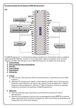
SlideShare a Scribd company logo
1
Q.1) Draw & Explain the Pin-Diagram of 8085 Microprocessor?
Ans:
The 8080 Microprocessor is an 8-bit general-purpose microprocessor having 40 pins which is capable of
addressing 64 kb of Memory .It works on +5v of single power-supply & can operate at the maximum
frequency of 5 MHz These 40 logic pin-out of 8085 Microprocessor are divided into 6 main groups.
1) Serial I/O Ports.
2) Interrupts & Externally-Initiated Signals.
3) Data-Bus.
4) Control Signals.
5) Status Signals.
6) Address Bus.
1) X1 & X2:
a) These are the 2 clock-input pins which are connected across a crystal RCLC Circuit of 6MHz
Frequency.
b) Whenever the microprocessor requires a clock-frequency of 3MHz, these 2 clock-input pins
divides the crystal-frequency into 2 parts in the internal circuitry & supplies the 1st 3MHz of
frequency to the microprocessor, while the 2nd 3MHz of Frequency is used as an operating
frequency to synchronize the operations of 8085 Microprocessor.
2) RESET OUT:
a) This is an active high output signal which is synchronized to the processor clock of
Microprocessor.
b) Whenever the microprocessor gets the reset-acknowledgement-signal R͞E͞S͞E͞T-I͞N, it sends the
output signal RESET-OUT to reset the microprocessor which resets all the connected devices &
indicates that the CPU has been Resetted.
2
3) SOD (Serial Output Data) pin:
a) It is an active high serial output line used for serial data communication.
b) It provides the data serially given by Microprocessor & delivers its output to the 7th bit of the
Accumulator when (Set Interrupt Mask) SIM instruction is executed.
4) SID (Serial Input Data) pin:
a) It is an active high Serial input data line used for serial data communication.
b) It accepts the serial-data & loads it into the 7th bit of the Accumulator whenever a (Read
Interrupt Mask) RIM instruction is executed.
5) TRAP:
a) This is an active, high-level, edge-triggered, non-maskable & highest priority interrupt.
b) It cannot be enabled or disabled using a program.
c) Whenever TRAP gets active, the program-counter of microprocessor automatically jumps to the
address 0024 respectively.
6) RST 7.5, RST 6.5, & RST 5.5:
These 3 pins are actively -high vectored maskable hardware restart interrupts.
They insert an internal restart function automatically which transfer the program-control to the
specific memory locations. It can be enabled or disabled using a program.
a) According to the priority, after the TRAP pin, the secondmost high-level pin is RST 7.5. This pin is
actively –high, vectored, edge-triggered, maskable hardware restart interrupts. When RST 7.5 is
active, the program counter jumps automatically at address 003C respectively.
b) After RST 7.5, the thirdmost high-level pin is RST 6.5. This pin is actively–high, vectored; level-
triggered, maskable hardware restart interrupts. When RST 6.5 is active, the program counter
jumps automatically at address 0034 respectively.
c) After RST 6.5, the forthmost high-level pin is RST 5.5. This pin is actively–high, vectored; level-
triggered, maskable hardware restart interrupts. When RST 6.5 is active, the program counter
jumps automatically at address 002C respectively.
7) INTR:
a) INTR is an active high, level-triggered, maskable, non-vectored, general-purpose hardware
interrupt pin.
b) It is a level-sensitive interrupt pin which has the lowest priority among the interrupts.
c) It can be enabled or disabled using a program.
d) If INTR is active, the Program Counter (PC) will be restricted from incrementing and it will
generate an interrupt acknowledge signal I͞N͞T͞A.
8) I͞N͞T͞A:
a) It is an active low, general-purpose interrupt acknowledgement signal.
b) Whenever the microprocessor receives interrupt signal, it is acknowledged by I͞N͞T͞A. So,
whenever the interrupt signal is received, I͞N͞T͞A goes high.
9) AD0-AD7:
a) These are the 8-bit bi-directional multiplexed, tri-state input pins which contains 2 sets of
signals 1) Address & 2) Data.
b) These set of lines used to carry the lower order 8-bit address as well as 8-bit data bus.
c) Here, the lower 8 bit of 16 bit address is multiplexed/time shared with data bus , because , at
one-time , 8-bit lower-address of memory is available on these lines & at another time the next
8-bit data is available.
3
10) VSS:
It is an interference pin which is connected to ground for avoiding ground-interference.
11) A8-A15:
These are the 8-bit uni-directional non-multiplexed, tri-state output pins used to carry higher order
address-signals of 16-bit Address.
12) S0 & S1:
These are status signals which provides different status and functions depending on their status.
IO/M̅ S0 S1 OPERATION
0 1 1 Opcode Fetch
0 0 1 Memory Read
0 1 0 Memory Write
1 0 1 I/O Read
1 1 0 I/O Write
1 0 1 Interrupt Acknowledge
Z 1 0 Halt
Z x x Hold
Z x x Reset
13) ALE:
a) ALE i.e Address Latch Enable is an output signal used to give information of AD0-AD7 Contents &
separate Address-Signals (A0-A7)& Data-Signals (D0-D7)fromAD0-AD7 pin.
b) It is a positive going pulse generated, when a new operation is started by Microprocessor.
c) When ALE is low, it indicates that the content on AD0-AD7 lines is the 8-bit data.
d) When ALE goes high, it indicates that the content on AD0-AD7 lines is in lower-order 8-bit
address of 16-bit address.
14) W͞͞R:
a) This is an active-low, output-control-signal pin used to write the data to the Memory or an I/O
Device.
b) Here, to write a data into a device/memory, microprocessor selects a device & then it transfers
the data & data-lines by generating W͞͞R signal from W͞͞R pin.
c) Thus, when the generated W͞͞R signal is low, then the data is readed from the I/O Device &
When the generated W͞͞R signal is high, then the data is readed from the Memory.
15) R͞D:
a) This is an active-low, output-control-signal pin used to read the data from the Memory or an I/O
Device.
b) Here, to read a data from a device/memory, microprocessor selects a device & then it transfers
the data & data-lines by generating R͞D signal from R͞D pin.
c) Thus, when the generated R͞D signal is low, then the data is readed from the I/O Device & When
the generated R͞D signal is high, then the data is readed from the Memory.
16) IO/M̅ :
a) It is a Status-Signal pin which distinguishes wheather the address is for Memory or to the I/O
Devices.
b) If IO/M͞ signal is low, then the Memory is Selected & If IO/M͞ signal is high, and then the I/O
Devices is selected.
4
17) READY :
a) It is an active-high, input-control signal pin used by the microprocessor to check wheather the
peripheral-devices is ready to transfer the data or not.
b) This signal is also used to synchronize slower peripheral-devices with the faster peripheral-
devices.
c) When READY Signal from READY pin is high, then the microprocessor completes the operation
& proceeds for next operation.
d) When READY Signal from READY pin is low, then the microprocessor will wait untill it goes high.
18) R͞E͞S͞E͞T-I͞N:
a) It is an active-low input reset-acknowledgement-signal used to reset the microprocessor & pass
an acknowledgement to RESET OUT signal which indicates that the CPU has been Resetted.
b) When this signal is received by the microprocessor, the address-lines, data-lines & control-lines
gets tri-stated & the memory-location of program-counter i.e 0000 is cleared along with the
flag-register & temporary-registers.
c) After this process, the program-counter is resetted where it starts executing from the Starting
memory-location 0000H onwards.
19) CLK:
a) It is output clock-signal which is used as a system-clock.
b) An Internally Operating 3MHz Frequency obtained from the crystally-connected clock-input pins
X1& X2 is stored in this pin which is used to operate other peripheral devices in the systemwith
the same speed.
20) HLDA:
It is an output-signal which indicates an acknowledgement to HOLD that the HOLD-Request has
been received.
21) HOLD:
a) HOLD is an active-high, input signal used by the DMA (Direct Memory Access) Controller to
transfer the data.
b) When a Peripheral Device wants to transfer the data, it requests DMA controller.
c) Here, in response with it , the DMA Controller ask for Buses to the 8085 Microprocessor by
making it’s HOLD output High which is connected to the Input of HOLD of Microprocessor.
d) Whenever the Microprocessor receives that high-output signal from HOLD’s input, then it sends
this high-output signal to HLDA to hold the acknowledgement that the HOLD-Request has been
received by the DMA Controller by indicating that it has turned the control over buses for other
master in the system.
e) When data-transfer is completed, then it returns the control of buses back to the 8085
Microprocessor by sending back a low HOLD Signal.
22) Vcc:
It is the main power-source pin which requires a single +5v of DC supply to run the 8085
Microprocessor.

More Related Content

What's hot

Memory & I/O interfacing
Memory & I/O  interfacingMemory & I/O  interfacing
Memory & I/O interfacing
deval patel
 
Timing diagram 8085 microprocessor
Timing diagram 8085 microprocessorTiming diagram 8085 microprocessor
Timing diagram 8085 microprocessor
Velalar College of Engineering and Technology
 
Assembly 8086
Assembly 8086Assembly 8086
Assembly 8086
Mustafa Salah
 
Advanced Comuter Architecture Ch6 Problem Solutions
Advanced Comuter Architecture Ch6 Problem SolutionsAdvanced Comuter Architecture Ch6 Problem Solutions
Advanced Comuter Architecture Ch6 Problem Solutions
Joe Christensen
 
8085 instruction set
8085 instruction set8085 instruction set
8086 MICROPROCESSOR
8086 MICROPROCESSOR8086 MICROPROCESSOR
8086 MICROPROCESSOR
Akhila Rahul
 
Minimum mode and Maximum mode Configuration in 8086
Minimum mode and Maximum mode Configuration in 8086Minimum mode and Maximum mode Configuration in 8086
Minimum mode and Maximum mode Configuration in 8086
Jismy .K.Jose
 
8085 Architecture & Memory Interfacing1
8085 Architecture & Memory Interfacing18085 Architecture & Memory Interfacing1
8085 Architecture & Memory Interfacing1
techbed
 
Lecture 5 Synchronous Sequential Logic
Lecture 5 Synchronous Sequential LogicLecture 5 Synchronous Sequential Logic
Lecture 5 Synchronous Sequential Logic
James Evangelos
 
Serial Communication in 8051
Serial Communication in 8051Serial Communication in 8051
Serial Communication in 8051
Sudhanshu Janwadkar
 
Clock-8086 bus cycle
Clock-8086 bus cycleClock-8086 bus cycle
Clock-8086 bus cycle
Rani Rahul
 
Combinational circuit
Combinational circuitCombinational circuit
Combinational circuit
Satya P. Joshi
 
Carry look ahead adder
Carry look ahead adderCarry look ahead adder
Carry look ahead adder
dragonpradeep
 
Programming with 8085
Programming with 8085Programming with 8085
Programming with 8085
Shehrevar Davierwala
 
3.programmable interrupt controller 8259
3.programmable interrupt controller 82593.programmable interrupt controller 8259
3.programmable interrupt controller 8259
MdFazleRabbi18
 
Architecture of 8085 microprocessor
Architecture of 8085 microprocessorArchitecture of 8085 microprocessor
Architecture of 8085 microprocessor
AMAN SRIVASTAVA
 
Register organization, stack
Register organization, stackRegister organization, stack
Register organization, stack
Asif Iqbal
 
Counters & time delay
Counters & time delayCounters & time delay
Counters & time delay
Hemant Chetwani
 
Unit 6 interprocessor arbitration
Unit 6 interprocessor arbitrationUnit 6 interprocessor arbitration
Unit 6 interprocessor arbitration
Dipesh Vaya
 
8051 ch9-950217
8051 ch9-9502178051 ch9-950217
8051 ch9-950217
Gopal Krishna Murthy C R
 

What's hot (20)

Memory & I/O interfacing
Memory & I/O  interfacingMemory & I/O  interfacing
Memory & I/O interfacing
 
Timing diagram 8085 microprocessor
Timing diagram 8085 microprocessorTiming diagram 8085 microprocessor
Timing diagram 8085 microprocessor
 
Assembly 8086
Assembly 8086Assembly 8086
Assembly 8086
 
Advanced Comuter Architecture Ch6 Problem Solutions
Advanced Comuter Architecture Ch6 Problem SolutionsAdvanced Comuter Architecture Ch6 Problem Solutions
Advanced Comuter Architecture Ch6 Problem Solutions
 
8085 instruction set
8085 instruction set8085 instruction set
8085 instruction set
 
8086 MICROPROCESSOR
8086 MICROPROCESSOR8086 MICROPROCESSOR
8086 MICROPROCESSOR
 
Minimum mode and Maximum mode Configuration in 8086
Minimum mode and Maximum mode Configuration in 8086Minimum mode and Maximum mode Configuration in 8086
Minimum mode and Maximum mode Configuration in 8086
 
8085 Architecture & Memory Interfacing1
8085 Architecture & Memory Interfacing18085 Architecture & Memory Interfacing1
8085 Architecture & Memory Interfacing1
 
Lecture 5 Synchronous Sequential Logic
Lecture 5 Synchronous Sequential LogicLecture 5 Synchronous Sequential Logic
Lecture 5 Synchronous Sequential Logic
 
Serial Communication in 8051
Serial Communication in 8051Serial Communication in 8051
Serial Communication in 8051
 
Clock-8086 bus cycle
Clock-8086 bus cycleClock-8086 bus cycle
Clock-8086 bus cycle
 
Combinational circuit
Combinational circuitCombinational circuit
Combinational circuit
 
Carry look ahead adder
Carry look ahead adderCarry look ahead adder
Carry look ahead adder
 
Programming with 8085
Programming with 8085Programming with 8085
Programming with 8085
 
3.programmable interrupt controller 8259
3.programmable interrupt controller 82593.programmable interrupt controller 8259
3.programmable interrupt controller 8259
 
Architecture of 8085 microprocessor
Architecture of 8085 microprocessorArchitecture of 8085 microprocessor
Architecture of 8085 microprocessor
 
Register organization, stack
Register organization, stackRegister organization, stack
Register organization, stack
 
Counters & time delay
Counters & time delayCounters & time delay
Counters & time delay
 
Unit 6 interprocessor arbitration
Unit 6 interprocessor arbitrationUnit 6 interprocessor arbitration
Unit 6 interprocessor arbitration
 
8051 ch9-950217
8051 ch9-9502178051 ch9-950217
8051 ch9-950217
 

Viewers also liked

Pin configuration of 8085
Pin configuration of 8085Pin configuration of 8085
Pin configuration of 8085
82338476
 
Bus structure of 8085 microprocessor 8085 microprocessor complete tutorial
Bus structure of 8085 microprocessor   8085 microprocessor complete tutorialBus structure of 8085 microprocessor   8085 microprocessor complete tutorial
Bus structure of 8085 microprocessor 8085 microprocessor complete tutorial
madhurace
 
8085 microproceesor ppt
8085 microproceesor ppt8085 microproceesor ppt
8085 microproceesor ppt
RJ Aniket
 
8085 full discription
8085 full discription8085 full discription
8085 full discription
Kartik Kalpande Patil
 
8085 microprocessor
8085 microprocessor8085 microprocessor
8085 microprocessor Architecture and pin description
8085 microprocessor Architecture and pin description 8085 microprocessor Architecture and pin description
8085 microprocessor Architecture and pin description
Vijay Kumar
 
8086 Microprocessor by Nitish Nagar
8086 Microprocessor by Nitish Nagar8086 Microprocessor by Nitish Nagar
8086 Microprocessor by Nitish Nagar
Nitish Nagar
 
Difference b/w 8085 & 8086
Difference b/w 8085 & 8086Difference b/w 8085 & 8086
Difference b/w 8085 & 8086
j4jiet
 
Detailed Explanation of Pin Description of 8085 microprocessor
Detailed Explanation of Pin Description of  8085 microprocessorDetailed Explanation of Pin Description of  8085 microprocessor
Detailed Explanation of Pin Description of 8085 microprocessor
Ramesh Dabhole
 
5.4 Data Bus
5.4 Data Bus5.4 Data Bus
5.4 Data Bus
lpapadop
 
Computer system bus
Computer system busComputer system bus
Computer system bus
Goran W. Hama Ali
 
8085 MICROPROCESSOR
8085 MICROPROCESSOR 8085 MICROPROCESSOR
8085 MICROPROCESSOR
THANDAIAH PRABU
 
Intro to Buses (Computer Architecture)
Intro to Buses  (Computer Architecture)Intro to Buses  (Computer Architecture)
Intro to Buses (Computer Architecture)
Matthew Levandowski
 
Unit 2 Principles of Programming Languages
Unit 2 Principles of Programming LanguagesUnit 2 Principles of Programming Languages
Unit 2 Principles of Programming Languages
Vasavi College of Engg
 
8085 microprocessor ramesh gaonkar
8085 microprocessor   ramesh gaonkar8085 microprocessor   ramesh gaonkar
8085 microprocessor ramesh gaonkar
SAQUIB AHMAD
 
Unit1 principle of programming language
Unit1 principle of programming languageUnit1 principle of programming language
Unit1 principle of programming language
Vasavi College of Engg
 
8085 microprocessor architecture ppt
8085 microprocessor architecture ppt8085 microprocessor architecture ppt
8085 microprocessor architecture ppt
Parvesh Gautam
 
Types of buses of computer
Types of buses of computerTypes of buses of computer
Types of buses of computer
SAGAR DODHIA
 

Viewers also liked (18)

Pin configuration of 8085
Pin configuration of 8085Pin configuration of 8085
Pin configuration of 8085
 
Bus structure of 8085 microprocessor 8085 microprocessor complete tutorial
Bus structure of 8085 microprocessor   8085 microprocessor complete tutorialBus structure of 8085 microprocessor   8085 microprocessor complete tutorial
Bus structure of 8085 microprocessor 8085 microprocessor complete tutorial
 
8085 microproceesor ppt
8085 microproceesor ppt8085 microproceesor ppt
8085 microproceesor ppt
 
8085 full discription
8085 full discription8085 full discription
8085 full discription
 
8085 microprocessor
8085 microprocessor8085 microprocessor
8085 microprocessor
 
8085 microprocessor Architecture and pin description
8085 microprocessor Architecture and pin description 8085 microprocessor Architecture and pin description
8085 microprocessor Architecture and pin description
 
8086 Microprocessor by Nitish Nagar
8086 Microprocessor by Nitish Nagar8086 Microprocessor by Nitish Nagar
8086 Microprocessor by Nitish Nagar
 
Difference b/w 8085 & 8086
Difference b/w 8085 & 8086Difference b/w 8085 & 8086
Difference b/w 8085 & 8086
 
Detailed Explanation of Pin Description of 8085 microprocessor
Detailed Explanation of Pin Description of  8085 microprocessorDetailed Explanation of Pin Description of  8085 microprocessor
Detailed Explanation of Pin Description of 8085 microprocessor
 
5.4 Data Bus
5.4 Data Bus5.4 Data Bus
5.4 Data Bus
 
Computer system bus
Computer system busComputer system bus
Computer system bus
 
8085 MICROPROCESSOR
8085 MICROPROCESSOR 8085 MICROPROCESSOR
8085 MICROPROCESSOR
 
Intro to Buses (Computer Architecture)
Intro to Buses  (Computer Architecture)Intro to Buses  (Computer Architecture)
Intro to Buses (Computer Architecture)
 
Unit 2 Principles of Programming Languages
Unit 2 Principles of Programming LanguagesUnit 2 Principles of Programming Languages
Unit 2 Principles of Programming Languages
 
8085 microprocessor ramesh gaonkar
8085 microprocessor   ramesh gaonkar8085 microprocessor   ramesh gaonkar
8085 microprocessor ramesh gaonkar
 
Unit1 principle of programming language
Unit1 principle of programming languageUnit1 principle of programming language
Unit1 principle of programming language
 
8085 microprocessor architecture ppt
8085 microprocessor architecture ppt8085 microprocessor architecture ppt
8085 microprocessor architecture ppt
 
Types of buses of computer
Types of buses of computerTypes of buses of computer
Types of buses of computer
 

Similar to 8085 microprocessor

8085_LAB_PROGRAMS.pdf
8085_LAB_PROGRAMS.pdf8085_LAB_PROGRAMS.pdf
8085_LAB_PROGRAMS.pdf
Koteswari Kasireddy
 
Application of 8086 and 8085 Microprocessor in Robots.pptx
Application of 8086 and 8085 Microprocessor in Robots.pptxApplication of 8086 and 8085 Microprocessor in Robots.pptx
Application of 8086 and 8085 Microprocessor in Robots.pptx
ssuser631ea0
 
Microprocessor Basics 8085 Ch-1
Microprocessor Basics 8085 Ch-1Microprocessor Basics 8085 Ch-1
Microprocessor Basics 8085 Ch-1
Neelam Kapoor
 
mic_unit1.pdf msbte unit 1 note pdf in ppt
mic_unit1.pdf msbte unit 1 note pdf in pptmic_unit1.pdf msbte unit 1 note pdf in ppt
mic_unit1.pdf msbte unit 1 note pdf in ppt
xboyxman1000
 
8086
80868086
Ju2416921695
Ju2416921695Ju2416921695
Ju2416921695
IJERA Editor
 
Microprocessor and Application (8085)
Microprocessor and Application (8085)Microprocessor and Application (8085)
Microprocessor and Application (8085)
ufaq kk
 
Assembler4
Assembler4Assembler4
Assembler4
Omar Sanchez
 
Pin Configuration.pptx
Pin Configuration.pptxPin Configuration.pptx
Pin Configuration.pptx
ssuser823c58
 
8085-microprocessor
8085-microprocessor8085-microprocessor
8085-microprocessor
ATTO RATHORE
 
UNIT 1 Microprocessors.pptx
UNIT 1 Microprocessors.pptxUNIT 1 Microprocessors.pptx
UNIT 1 Microprocessors.pptx
Gowrishankar C
 
8085 microprocessor
8085 microprocessor8085 microprocessor
8085 microprocessor
GurleenKaur408
 
Obstacle Avoidance Robotic Vehicle
Obstacle Avoidance Robotic VehicleObstacle Avoidance Robotic Vehicle
Obstacle Avoidance Robotic Vehicle
Edgefxkits & Solutions
 
8086 pin details
8086 pin details8086 pin details
8086 pin details
AJAL A J
 
Coin based mobile charger project report
Coin based mobile charger project reportCoin based mobile charger project report
Coin based mobile charger project report
kaushal chaubey
 
8086 new
8086 new8086 new
Presentation of pin diagram
Presentation of pin diagramPresentation of pin diagram
Presentation of pin diagram
Rohitkumar3723
 
UNIT 2.pptx
UNIT 2.pptxUNIT 2.pptx
UNIT 2.pptx
BASKARS53
 
8086 complete guide
8086 complete guide 8086 complete guide
8086 complete guide
SHREEHARI WADAWADAGI
 
Pin diagram of 8085
Pin diagram of 8085Pin diagram of 8085
Pin diagram of 8085
ShivamSood22
 

Similar to 8085 microprocessor (20)

8085_LAB_PROGRAMS.pdf
8085_LAB_PROGRAMS.pdf8085_LAB_PROGRAMS.pdf
8085_LAB_PROGRAMS.pdf
 
Application of 8086 and 8085 Microprocessor in Robots.pptx
Application of 8086 and 8085 Microprocessor in Robots.pptxApplication of 8086 and 8085 Microprocessor in Robots.pptx
Application of 8086 and 8085 Microprocessor in Robots.pptx
 
Microprocessor Basics 8085 Ch-1
Microprocessor Basics 8085 Ch-1Microprocessor Basics 8085 Ch-1
Microprocessor Basics 8085 Ch-1
 
mic_unit1.pdf msbte unit 1 note pdf in ppt
mic_unit1.pdf msbte unit 1 note pdf in pptmic_unit1.pdf msbte unit 1 note pdf in ppt
mic_unit1.pdf msbte unit 1 note pdf in ppt
 
8086
80868086
8086
 
Ju2416921695
Ju2416921695Ju2416921695
Ju2416921695
 
Microprocessor and Application (8085)
Microprocessor and Application (8085)Microprocessor and Application (8085)
Microprocessor and Application (8085)
 
Assembler4
Assembler4Assembler4
Assembler4
 
Pin Configuration.pptx
Pin Configuration.pptxPin Configuration.pptx
Pin Configuration.pptx
 
8085-microprocessor
8085-microprocessor8085-microprocessor
8085-microprocessor
 
UNIT 1 Microprocessors.pptx
UNIT 1 Microprocessors.pptxUNIT 1 Microprocessors.pptx
UNIT 1 Microprocessors.pptx
 
8085 microprocessor
8085 microprocessor8085 microprocessor
8085 microprocessor
 
Obstacle Avoidance Robotic Vehicle
Obstacle Avoidance Robotic VehicleObstacle Avoidance Robotic Vehicle
Obstacle Avoidance Robotic Vehicle
 
8086 pin details
8086 pin details8086 pin details
8086 pin details
 
Coin based mobile charger project report
Coin based mobile charger project reportCoin based mobile charger project report
Coin based mobile charger project report
 
8086 new
8086 new8086 new
8086 new
 
Presentation of pin diagram
Presentation of pin diagramPresentation of pin diagram
Presentation of pin diagram
 
UNIT 2.pptx
UNIT 2.pptxUNIT 2.pptx
UNIT 2.pptx
 
8086 complete guide
8086 complete guide 8086 complete guide
8086 complete guide
 
Pin diagram of 8085
Pin diagram of 8085Pin diagram of 8085
Pin diagram of 8085
 

Recently uploaded

bank management system in java and mysql report1.pdf
bank management system in java and mysql report1.pdfbank management system in java and mysql report1.pdf
bank management system in java and mysql report1.pdf
Divyam548318
 
Generative AI leverages algorithms to create various forms of content
Generative AI leverages algorithms to create various forms of contentGenerative AI leverages algorithms to create various forms of content
Generative AI leverages algorithms to create various forms of content
Hitesh Mohapatra
 
CHINA’S GEO-ECONOMIC OUTREACH IN CENTRAL ASIAN COUNTRIES AND FUTURE PROSPECT
CHINA’S GEO-ECONOMIC OUTREACH IN CENTRAL ASIAN COUNTRIES AND FUTURE PROSPECTCHINA’S GEO-ECONOMIC OUTREACH IN CENTRAL ASIAN COUNTRIES AND FUTURE PROSPECT
CHINA’S GEO-ECONOMIC OUTREACH IN CENTRAL ASIAN COUNTRIES AND FUTURE PROSPECT
jpsjournal1
 
BPV-GUI-01-Guide-for-ASME-Review-Teams-(General)-10-10-2023.pdf
BPV-GUI-01-Guide-for-ASME-Review-Teams-(General)-10-10-2023.pdfBPV-GUI-01-Guide-for-ASME-Review-Teams-(General)-10-10-2023.pdf
BPV-GUI-01-Guide-for-ASME-Review-Teams-(General)-10-10-2023.pdf
MIGUELANGEL966976
 
Series of visio cisco devices Cisco_Icons.ppt
Series of visio cisco devices Cisco_Icons.pptSeries of visio cisco devices Cisco_Icons.ppt
Series of visio cisco devices Cisco_Icons.ppt
PauloRodrigues104553
 
Modelagem de um CSTR com reação endotermica.pdf
Modelagem de um CSTR com reação endotermica.pdfModelagem de um CSTR com reação endotermica.pdf
Modelagem de um CSTR com reação endotermica.pdf
camseq
 
CSM Cloud Service Management Presentarion
CSM Cloud Service Management PresentarionCSM Cloud Service Management Presentarion
CSM Cloud Service Management Presentarion
rpskprasana
 
5214-1693458878915-Unit 6 2023 to 2024 academic year assignment (AutoRecovere...
5214-1693458878915-Unit 6 2023 to 2024 academic year assignment (AutoRecovere...5214-1693458878915-Unit 6 2023 to 2024 academic year assignment (AutoRecovere...
5214-1693458878915-Unit 6 2023 to 2024 academic year assignment (AutoRecovere...
ihlasbinance2003
 
14 Template Contractual Notice - EOT Application
14 Template Contractual Notice - EOT Application14 Template Contractual Notice - EOT Application
14 Template Contractual Notice - EOT Application
SyedAbiiAzazi1
 
Understanding Inductive Bias in Machine Learning
Understanding Inductive Bias in Machine LearningUnderstanding Inductive Bias in Machine Learning
Understanding Inductive Bias in Machine Learning
SUTEJAS
 
Iron and Steel Technology Roadmap - Towards more sustainable steelmaking.pdf
Iron and Steel Technology Roadmap - Towards more sustainable steelmaking.pdfIron and Steel Technology Roadmap - Towards more sustainable steelmaking.pdf
Iron and Steel Technology Roadmap - Towards more sustainable steelmaking.pdf
RadiNasr
 
digital fundamental by Thomas L.floydl.pdf
digital fundamental by Thomas L.floydl.pdfdigital fundamental by Thomas L.floydl.pdf
digital fundamental by Thomas L.floydl.pdf
drwaing
 
132/33KV substation case study Presentation
132/33KV substation case study Presentation132/33KV substation case study Presentation
132/33KV substation case study Presentation
kandramariana6
 
Advanced control scheme of doubly fed induction generator for wind turbine us...
Advanced control scheme of doubly fed induction generator for wind turbine us...Advanced control scheme of doubly fed induction generator for wind turbine us...
Advanced control scheme of doubly fed induction generator for wind turbine us...
IJECEIAES
 
Embedded machine learning-based road conditions and driving behavior monitoring
Embedded machine learning-based road conditions and driving behavior monitoringEmbedded machine learning-based road conditions and driving behavior monitoring
Embedded machine learning-based road conditions and driving behavior monitoring
IJECEIAES
 
Recycled Concrete Aggregate in Construction Part III
Recycled Concrete Aggregate in Construction Part IIIRecycled Concrete Aggregate in Construction Part III
Recycled Concrete Aggregate in Construction Part III
Aditya Rajan Patra
 
RAT: Retrieval Augmented Thoughts Elicit Context-Aware Reasoning in Long-Hori...
RAT: Retrieval Augmented Thoughts Elicit Context-Aware Reasoning in Long-Hori...RAT: Retrieval Augmented Thoughts Elicit Context-Aware Reasoning in Long-Hori...
RAT: Retrieval Augmented Thoughts Elicit Context-Aware Reasoning in Long-Hori...
thanhdowork
 
6th International Conference on Machine Learning & Applications (CMLA 2024)
6th International Conference on Machine Learning & Applications (CMLA 2024)6th International Conference on Machine Learning & Applications (CMLA 2024)
6th International Conference on Machine Learning & Applications (CMLA 2024)
ClaraZara1
 
Question paper of renewable energy sources
Question paper of renewable energy sourcesQuestion paper of renewable energy sources
Question paper of renewable energy sources
mahammadsalmanmech
 
DEEP LEARNING FOR SMART GRID INTRUSION DETECTION: A HYBRID CNN-LSTM-BASED MODEL
DEEP LEARNING FOR SMART GRID INTRUSION DETECTION: A HYBRID CNN-LSTM-BASED MODELDEEP LEARNING FOR SMART GRID INTRUSION DETECTION: A HYBRID CNN-LSTM-BASED MODEL
DEEP LEARNING FOR SMART GRID INTRUSION DETECTION: A HYBRID CNN-LSTM-BASED MODEL
gerogepatton
 

Recently uploaded (20)

bank management system in java and mysql report1.pdf
bank management system in java and mysql report1.pdfbank management system in java and mysql report1.pdf
bank management system in java and mysql report1.pdf
 
Generative AI leverages algorithms to create various forms of content
Generative AI leverages algorithms to create various forms of contentGenerative AI leverages algorithms to create various forms of content
Generative AI leverages algorithms to create various forms of content
 
CHINA’S GEO-ECONOMIC OUTREACH IN CENTRAL ASIAN COUNTRIES AND FUTURE PROSPECT
CHINA’S GEO-ECONOMIC OUTREACH IN CENTRAL ASIAN COUNTRIES AND FUTURE PROSPECTCHINA’S GEO-ECONOMIC OUTREACH IN CENTRAL ASIAN COUNTRIES AND FUTURE PROSPECT
CHINA’S GEO-ECONOMIC OUTREACH IN CENTRAL ASIAN COUNTRIES AND FUTURE PROSPECT
 
BPV-GUI-01-Guide-for-ASME-Review-Teams-(General)-10-10-2023.pdf
BPV-GUI-01-Guide-for-ASME-Review-Teams-(General)-10-10-2023.pdfBPV-GUI-01-Guide-for-ASME-Review-Teams-(General)-10-10-2023.pdf
BPV-GUI-01-Guide-for-ASME-Review-Teams-(General)-10-10-2023.pdf
 
Series of visio cisco devices Cisco_Icons.ppt
Series of visio cisco devices Cisco_Icons.pptSeries of visio cisco devices Cisco_Icons.ppt
Series of visio cisco devices Cisco_Icons.ppt
 
Modelagem de um CSTR com reação endotermica.pdf
Modelagem de um CSTR com reação endotermica.pdfModelagem de um CSTR com reação endotermica.pdf
Modelagem de um CSTR com reação endotermica.pdf
 
CSM Cloud Service Management Presentarion
CSM Cloud Service Management PresentarionCSM Cloud Service Management Presentarion
CSM Cloud Service Management Presentarion
 
5214-1693458878915-Unit 6 2023 to 2024 academic year assignment (AutoRecovere...
5214-1693458878915-Unit 6 2023 to 2024 academic year assignment (AutoRecovere...5214-1693458878915-Unit 6 2023 to 2024 academic year assignment (AutoRecovere...
5214-1693458878915-Unit 6 2023 to 2024 academic year assignment (AutoRecovere...
 
14 Template Contractual Notice - EOT Application
14 Template Contractual Notice - EOT Application14 Template Contractual Notice - EOT Application
14 Template Contractual Notice - EOT Application
 
Understanding Inductive Bias in Machine Learning
Understanding Inductive Bias in Machine LearningUnderstanding Inductive Bias in Machine Learning
Understanding Inductive Bias in Machine Learning
 
Iron and Steel Technology Roadmap - Towards more sustainable steelmaking.pdf
Iron and Steel Technology Roadmap - Towards more sustainable steelmaking.pdfIron and Steel Technology Roadmap - Towards more sustainable steelmaking.pdf
Iron and Steel Technology Roadmap - Towards more sustainable steelmaking.pdf
 
digital fundamental by Thomas L.floydl.pdf
digital fundamental by Thomas L.floydl.pdfdigital fundamental by Thomas L.floydl.pdf
digital fundamental by Thomas L.floydl.pdf
 
132/33KV substation case study Presentation
132/33KV substation case study Presentation132/33KV substation case study Presentation
132/33KV substation case study Presentation
 
Advanced control scheme of doubly fed induction generator for wind turbine us...
Advanced control scheme of doubly fed induction generator for wind turbine us...Advanced control scheme of doubly fed induction generator for wind turbine us...
Advanced control scheme of doubly fed induction generator for wind turbine us...
 
Embedded machine learning-based road conditions and driving behavior monitoring
Embedded machine learning-based road conditions and driving behavior monitoringEmbedded machine learning-based road conditions and driving behavior monitoring
Embedded machine learning-based road conditions and driving behavior monitoring
 
Recycled Concrete Aggregate in Construction Part III
Recycled Concrete Aggregate in Construction Part IIIRecycled Concrete Aggregate in Construction Part III
Recycled Concrete Aggregate in Construction Part III
 
RAT: Retrieval Augmented Thoughts Elicit Context-Aware Reasoning in Long-Hori...
RAT: Retrieval Augmented Thoughts Elicit Context-Aware Reasoning in Long-Hori...RAT: Retrieval Augmented Thoughts Elicit Context-Aware Reasoning in Long-Hori...
RAT: Retrieval Augmented Thoughts Elicit Context-Aware Reasoning in Long-Hori...
 
6th International Conference on Machine Learning & Applications (CMLA 2024)
6th International Conference on Machine Learning & Applications (CMLA 2024)6th International Conference on Machine Learning & Applications (CMLA 2024)
6th International Conference on Machine Learning & Applications (CMLA 2024)
 
Question paper of renewable energy sources
Question paper of renewable energy sourcesQuestion paper of renewable energy sources
Question paper of renewable energy sources
 
DEEP LEARNING FOR SMART GRID INTRUSION DETECTION: A HYBRID CNN-LSTM-BASED MODEL
DEEP LEARNING FOR SMART GRID INTRUSION DETECTION: A HYBRID CNN-LSTM-BASED MODELDEEP LEARNING FOR SMART GRID INTRUSION DETECTION: A HYBRID CNN-LSTM-BASED MODEL
DEEP LEARNING FOR SMART GRID INTRUSION DETECTION: A HYBRID CNN-LSTM-BASED MODEL
 

8085 microprocessor

  • 1. 1 Q.1) Draw & Explain the Pin-Diagram of 8085 Microprocessor? Ans: The 8080 Microprocessor is an 8-bit general-purpose microprocessor having 40 pins which is capable of addressing 64 kb of Memory .It works on +5v of single power-supply & can operate at the maximum frequency of 5 MHz These 40 logic pin-out of 8085 Microprocessor are divided into 6 main groups. 1) Serial I/O Ports. 2) Interrupts & Externally-Initiated Signals. 3) Data-Bus. 4) Control Signals. 5) Status Signals. 6) Address Bus. 1) X1 & X2: a) These are the 2 clock-input pins which are connected across a crystal RCLC Circuit of 6MHz Frequency. b) Whenever the microprocessor requires a clock-frequency of 3MHz, these 2 clock-input pins divides the crystal-frequency into 2 parts in the internal circuitry & supplies the 1st 3MHz of frequency to the microprocessor, while the 2nd 3MHz of Frequency is used as an operating frequency to synchronize the operations of 8085 Microprocessor. 2) RESET OUT: a) This is an active high output signal which is synchronized to the processor clock of Microprocessor. b) Whenever the microprocessor gets the reset-acknowledgement-signal R͞E͞S͞E͞T-I͞N, it sends the output signal RESET-OUT to reset the microprocessor which resets all the connected devices & indicates that the CPU has been Resetted.
  • 2. 2 3) SOD (Serial Output Data) pin: a) It is an active high serial output line used for serial data communication. b) It provides the data serially given by Microprocessor & delivers its output to the 7th bit of the Accumulator when (Set Interrupt Mask) SIM instruction is executed. 4) SID (Serial Input Data) pin: a) It is an active high Serial input data line used for serial data communication. b) It accepts the serial-data & loads it into the 7th bit of the Accumulator whenever a (Read Interrupt Mask) RIM instruction is executed. 5) TRAP: a) This is an active, high-level, edge-triggered, non-maskable & highest priority interrupt. b) It cannot be enabled or disabled using a program. c) Whenever TRAP gets active, the program-counter of microprocessor automatically jumps to the address 0024 respectively. 6) RST 7.5, RST 6.5, & RST 5.5: These 3 pins are actively -high vectored maskable hardware restart interrupts. They insert an internal restart function automatically which transfer the program-control to the specific memory locations. It can be enabled or disabled using a program. a) According to the priority, after the TRAP pin, the secondmost high-level pin is RST 7.5. This pin is actively –high, vectored, edge-triggered, maskable hardware restart interrupts. When RST 7.5 is active, the program counter jumps automatically at address 003C respectively. b) After RST 7.5, the thirdmost high-level pin is RST 6.5. This pin is actively–high, vectored; level- triggered, maskable hardware restart interrupts. When RST 6.5 is active, the program counter jumps automatically at address 0034 respectively. c) After RST 6.5, the forthmost high-level pin is RST 5.5. This pin is actively–high, vectored; level- triggered, maskable hardware restart interrupts. When RST 6.5 is active, the program counter jumps automatically at address 002C respectively. 7) INTR: a) INTR is an active high, level-triggered, maskable, non-vectored, general-purpose hardware interrupt pin. b) It is a level-sensitive interrupt pin which has the lowest priority among the interrupts. c) It can be enabled or disabled using a program. d) If INTR is active, the Program Counter (PC) will be restricted from incrementing and it will generate an interrupt acknowledge signal I͞N͞T͞A. 8) I͞N͞T͞A: a) It is an active low, general-purpose interrupt acknowledgement signal. b) Whenever the microprocessor receives interrupt signal, it is acknowledged by I͞N͞T͞A. So, whenever the interrupt signal is received, I͞N͞T͞A goes high. 9) AD0-AD7: a) These are the 8-bit bi-directional multiplexed, tri-state input pins which contains 2 sets of signals 1) Address & 2) Data. b) These set of lines used to carry the lower order 8-bit address as well as 8-bit data bus. c) Here, the lower 8 bit of 16 bit address is multiplexed/time shared with data bus , because , at one-time , 8-bit lower-address of memory is available on these lines & at another time the next 8-bit data is available.
  • 3. 3 10) VSS: It is an interference pin which is connected to ground for avoiding ground-interference. 11) A8-A15: These are the 8-bit uni-directional non-multiplexed, tri-state output pins used to carry higher order address-signals of 16-bit Address. 12) S0 & S1: These are status signals which provides different status and functions depending on their status. IO/M̅ S0 S1 OPERATION 0 1 1 Opcode Fetch 0 0 1 Memory Read 0 1 0 Memory Write 1 0 1 I/O Read 1 1 0 I/O Write 1 0 1 Interrupt Acknowledge Z 1 0 Halt Z x x Hold Z x x Reset 13) ALE: a) ALE i.e Address Latch Enable is an output signal used to give information of AD0-AD7 Contents & separate Address-Signals (A0-A7)& Data-Signals (D0-D7)fromAD0-AD7 pin. b) It is a positive going pulse generated, when a new operation is started by Microprocessor. c) When ALE is low, it indicates that the content on AD0-AD7 lines is the 8-bit data. d) When ALE goes high, it indicates that the content on AD0-AD7 lines is in lower-order 8-bit address of 16-bit address. 14) W͞͞R: a) This is an active-low, output-control-signal pin used to write the data to the Memory or an I/O Device. b) Here, to write a data into a device/memory, microprocessor selects a device & then it transfers the data & data-lines by generating W͞͞R signal from W͞͞R pin. c) Thus, when the generated W͞͞R signal is low, then the data is readed from the I/O Device & When the generated W͞͞R signal is high, then the data is readed from the Memory. 15) R͞D: a) This is an active-low, output-control-signal pin used to read the data from the Memory or an I/O Device. b) Here, to read a data from a device/memory, microprocessor selects a device & then it transfers the data & data-lines by generating R͞D signal from R͞D pin. c) Thus, when the generated R͞D signal is low, then the data is readed from the I/O Device & When the generated R͞D signal is high, then the data is readed from the Memory. 16) IO/M̅ : a) It is a Status-Signal pin which distinguishes wheather the address is for Memory or to the I/O Devices. b) If IO/M͞ signal is low, then the Memory is Selected & If IO/M͞ signal is high, and then the I/O Devices is selected.
  • 4. 4 17) READY : a) It is an active-high, input-control signal pin used by the microprocessor to check wheather the peripheral-devices is ready to transfer the data or not. b) This signal is also used to synchronize slower peripheral-devices with the faster peripheral- devices. c) When READY Signal from READY pin is high, then the microprocessor completes the operation & proceeds for next operation. d) When READY Signal from READY pin is low, then the microprocessor will wait untill it goes high. 18) R͞E͞S͞E͞T-I͞N: a) It is an active-low input reset-acknowledgement-signal used to reset the microprocessor & pass an acknowledgement to RESET OUT signal which indicates that the CPU has been Resetted. b) When this signal is received by the microprocessor, the address-lines, data-lines & control-lines gets tri-stated & the memory-location of program-counter i.e 0000 is cleared along with the flag-register & temporary-registers. c) After this process, the program-counter is resetted where it starts executing from the Starting memory-location 0000H onwards. 19) CLK: a) It is output clock-signal which is used as a system-clock. b) An Internally Operating 3MHz Frequency obtained from the crystally-connected clock-input pins X1& X2 is stored in this pin which is used to operate other peripheral devices in the systemwith the same speed. 20) HLDA: It is an output-signal which indicates an acknowledgement to HOLD that the HOLD-Request has been received. 21) HOLD: a) HOLD is an active-high, input signal used by the DMA (Direct Memory Access) Controller to transfer the data. b) When a Peripheral Device wants to transfer the data, it requests DMA controller. c) Here, in response with it , the DMA Controller ask for Buses to the 8085 Microprocessor by making it’s HOLD output High which is connected to the Input of HOLD of Microprocessor. d) Whenever the Microprocessor receives that high-output signal from HOLD’s input, then it sends this high-output signal to HLDA to hold the acknowledgement that the HOLD-Request has been received by the DMA Controller by indicating that it has turned the control over buses for other master in the system. e) When data-transfer is completed, then it returns the control of buses back to the 8085 Microprocessor by sending back a low HOLD Signal. 22) Vcc: It is the main power-source pin which requires a single +5v of DC supply to run the 8085 Microprocessor.