A detailed overview of Sierra Monitor's FieldServer protocol gateways for original equipment manufacturers (OEMs). This covers the FieldServer OEM product line, features and benefits of working with us, and use cases.
A detailed overview of Sierra Monitor's FieldServer protocol gateways for integrators. This covers the FieldServer product line, features, and building automation use cases.
MIPI DevCon 2016: Accelerating Software Development for MIPI CSI-2 CamerasMIPI Alliance
MIPI CSI-2-compliant cameras are popular in mobile and mobile-influenced devices because of the specification’s ability to handle high image resolution over fast links with low-power consumption. SoC designers can accelerate their design process by integrating the software drivers to make initial development easier and directly control boot-up sequences. This presentation by Licinio Sousa of Synopsys describes how to use the existing host-side V4L2 API and V4L2 subdevice interfaces to ease the integration of a CSI-2-compliant camera with an existing system. This approach allows designers to easily change their camera without having to make any changes to the CSI-2 host driver.
Contents are following
• Product Overview
• Hardware Specification
• Software Service
• IP-PBX Service and Features
• RTP Proxy Service
• User Presence Service
• System Redundancy
• Network Service and Features
• User Terminals
• Application Area
International Journal of Computational Engineering Research(IJCER)ijceronline
International Journal of Computational Engineering Research(IJCER) is an intentional online Journal in English monthly publishing journal. This Journal publish original research work that contributes significantly to further the scientific knowledge in engineering and Technology.
[Advantech] PAC SW Multiprog Tutorial step by step Ming-Hung Hseih
This is tutorial to give you basic concept and how to program PAC Software Multuprog.
•Level 1 : Create a new project and link test
•Level 2: IO configuration -IO slot
•Level 3 : IO configuration -Modbus client and
•Level 4 : IO configuration -Shared memory
•Level 5 : KW Program -R/W data and define user function
•Level 6 : KW Program -Modbus client and server expert
•Level 7 : KW Program -Do it !
PCIe Gen 3.0 Presentation @ 4th FPGA CampFPGA Central
PCIe Gen3 presentation by PLDA at 4th FPGA Camp in Santa Clara, CA. For more details visit http://www.fpgacentral.com/fpgacamp or http://www.fpgacentral.com
Rhino labs Prese4th ntation At FPGA Camp, Santa Clara, CAFPGA Central
Presentation by Guy Marom of Rhino Labs at the 4th FPGA Camp in Santa Clara.
More details visit http://www.fpgacentral.com/fpgacamp or http://www.fpgacentral.com
In This PPT we are discussed about complete details of that product (Use,Operation, Technical details, Dimensions, Wiring, and etc..)
Please Support us and Follow our other Sites
https://automationtechplc2.blogspot.com
https://humidificationcontrol.blogspot.com
https://controlsandsystems.business.site
If you enjoyed this article, share it with your friends and colleagues
Using a Field Programmable Gate Array to Accelerate Application PerformanceOdinot Stanislas
Intel s'intéresse tout particulièrement aux FPGA et notamment au potentiel qu'ils apportent lorsque les ISV et développeurs ont des besoins très spécifiques en Génomique, traitement d'images, traitement de bases de données, et même dans le Cloud. Dans ce document vous aurez l'occasion d'en savoir plus sur notre stratégie, et sur un programme de recherche lancé par Intel et Altera impliquant des Xeon E5 équipés... de FPGA
Intel is looking at FPGA and what they bring to ISVs and developers and their very specific needs in genomics, image processing, databases, and even in the cloud. In this document you will have the opportunity to learn more about our strategy, and a research program initiated by Intel and Altera involving Xeon E5 with... FPGA inside.
Auteur(s)/Author(s):
P. K. Gupta, Director of Cloud Platform Technology, Intel Corporation
ASIC Implementation of I2C Master bus controller with design of Firm IP core has been proposed in this paper. I2C is one the most prominent protocol used in on chip communication among sub-systems. The generic design of I2C master controller has ample of features to incorporate vast varieties of application and I2C standards. The generic design is slow, congested and require high power. It’s rare to utilize all the
features of generic design fully in a single particular application or system. Hence, a modified ASIC design
with specific less features but with better timing, low power requirement and less area overhead, has been
proposed in this paper. This design is specifically apt for digital systems which have serial bus interface
requirement for on board communication. Moreover, the Firm IP core of I2C Master Controller has been designed for ASIC, which makes the design highly portable on any ASIC chips or SOC designs. The firm IPs is best in terms of flexibility and more predictable than commonly found soft IPs. The entire custom ASIC implementation of proposed design has been done in Cadence Tool chain with 45nm technology using
standard cell library. A thorough comparison has been done between generic open sourced RTL design of I2C Controller obtained from Opencores.org and our proposed design.
UiPath Test Automation using UiPath Test Suite series, part 4DianaGray10
Welcome to UiPath Test Automation using UiPath Test Suite series part 4. In this session, we will cover Test Manager overview along with SAP heatmap.
The UiPath Test Manager overview with SAP heatmap webinar offers a concise yet comprehensive exploration of the role of a Test Manager within SAP environments, coupled with the utilization of heatmaps for effective testing strategies.
Participants will gain insights into the responsibilities, challenges, and best practices associated with test management in SAP projects. Additionally, the webinar delves into the significance of heatmaps as a visual aid for identifying testing priorities, areas of risk, and resource allocation within SAP landscapes. Through this session, attendees can expect to enhance their understanding of test management principles while learning practical approaches to optimize testing processes in SAP environments using heatmap visualization techniques
What will you get from this session?
1. Insights into SAP testing best practices
2. Heatmap utilization for testing
3. Optimization of testing processes
4. Demo
Topics covered:
Execution from the test manager
Orchestrator execution result
Defect reporting
SAP heatmap example with demo
Speaker:
Deepak Rai, Automation Practice Lead, Boundaryless Group and UiPath MVP
GraphRAG is All You need? LLM & Knowledge GraphGuy Korland
Guy Korland, CEO and Co-founder of FalkorDB, will review two articles on the integration of language models with knowledge graphs.
1. Unifying Large Language Models and Knowledge Graphs: A Roadmap.
https://arxiv.org/abs/2306.08302
2. Microsoft Research's GraphRAG paper and a review paper on various uses of knowledge graphs:
https://www.microsoft.com/en-us/research/blog/graphrag-unlocking-llm-discovery-on-narrative-private-data/
LF Energy Webinar: Electrical Grid Modelling and Simulation Through PowSyBl -...DanBrown980551
Do you want to learn how to model and simulate an electrical network from scratch in under an hour?
Then welcome to this PowSyBl workshop, hosted by Rte, the French Transmission System Operator (TSO)!
During the webinar, you will discover the PowSyBl ecosystem as well as handle and study an electrical network through an interactive Python notebook.
PowSyBl is an open source project hosted by LF Energy, which offers a comprehensive set of features for electrical grid modelling and simulation. Among other advanced features, PowSyBl provides:
- A fully editable and extendable library for grid component modelling;
- Visualization tools to display your network;
- Grid simulation tools, such as power flows, security analyses (with or without remedial actions) and sensitivity analyses;
The framework is mostly written in Java, with a Python binding so that Python developers can access PowSyBl functionalities as well.
What you will learn during the webinar:
- For beginners: discover PowSyBl's functionalities through a quick general presentation and the notebook, without needing any expert coding skills;
- For advanced developers: master the skills to efficiently apply PowSyBl functionalities to your real-world scenarios.
Transcript: Selling digital books in 2024: Insights from industry leaders - T...BookNet Canada
The publishing industry has been selling digital audiobooks and ebooks for over a decade and has found its groove. What’s changed? What has stayed the same? Where do we go from here? Join a group of leading sales peers from across the industry for a conversation about the lessons learned since the popularization of digital books, best practices, digital book supply chain management, and more.
Link to video recording: https://bnctechforum.ca/sessions/selling-digital-books-in-2024-insights-from-industry-leaders/
Presented by BookNet Canada on May 28, 2024, with support from the Department of Canadian Heritage.
JMeter webinar - integration with InfluxDB and GrafanaRTTS
Watch this recorded webinar about real-time monitoring of application performance. See how to integrate Apache JMeter, the open-source leader in performance testing, with InfluxDB, the open-source time-series database, and Grafana, the open-source analytics and visualization application.
In this webinar, we will review the benefits of leveraging InfluxDB and Grafana when executing load tests and demonstrate how these tools are used to visualize performance metrics.
Length: 30 minutes
Session Overview
-------------------------------------------
During this webinar, we will cover the following topics while demonstrating the integrations of JMeter, InfluxDB and Grafana:
- What out-of-the-box solutions are available for real-time monitoring JMeter tests?
- What are the benefits of integrating InfluxDB and Grafana into the load testing stack?
- Which features are provided by Grafana?
- Demonstration of InfluxDB and Grafana using a practice web application
To view the webinar recording, go to:
https://www.rttsweb.com/jmeter-integration-webinar
Essentials of Automations: Optimizing FME Workflows with ParametersSafe Software
Are you looking to streamline your workflows and boost your projects’ efficiency? Do you find yourself searching for ways to add flexibility and control over your FME workflows? If so, you’re in the right place.
Join us for an insightful dive into the world of FME parameters, a critical element in optimizing workflow efficiency. This webinar marks the beginning of our three-part “Essentials of Automation” series. This first webinar is designed to equip you with the knowledge and skills to utilize parameters effectively: enhancing the flexibility, maintainability, and user control of your FME projects.
Here’s what you’ll gain:
- Essentials of FME Parameters: Understand the pivotal role of parameters, including Reader/Writer, Transformer, User, and FME Flow categories. Discover how they are the key to unlocking automation and optimization within your workflows.
- Practical Applications in FME Form: Delve into key user parameter types including choice, connections, and file URLs. Allow users to control how a workflow runs, making your workflows more reusable. Learn to import values and deliver the best user experience for your workflows while enhancing accuracy.
- Optimization Strategies in FME Flow: Explore the creation and strategic deployment of parameters in FME Flow, including the use of deployment and geometry parameters, to maximize workflow efficiency.
- Pro Tips for Success: Gain insights on parameterizing connections and leveraging new features like Conditional Visibility for clarity and simplicity.
We’ll wrap up with a glimpse into future webinars, followed by a Q&A session to address your specific questions surrounding this topic.
Don’t miss this opportunity to elevate your FME expertise and drive your projects to new heights of efficiency.
Epistemic Interaction - tuning interfaces to provide information for AI supportAlan Dix
Paper presented at SYNERGY workshop at AVI 2024, Genoa, Italy. 3rd June 2024
https://alandix.com/academic/papers/synergy2024-epistemic/
As machine learning integrates deeper into human-computer interactions, the concept of epistemic interaction emerges, aiming to refine these interactions to enhance system adaptability. This approach encourages minor, intentional adjustments in user behaviour to enrich the data available for system learning. This paper introduces epistemic interaction within the context of human-system communication, illustrating how deliberate interaction design can improve system understanding and adaptation. Through concrete examples, we demonstrate the potential of epistemic interaction to significantly advance human-computer interaction by leveraging intuitive human communication strategies to inform system design and functionality, offering a novel pathway for enriching user-system engagements.
DevOps and Testing slides at DASA ConnectKari Kakkonen
My and Rik Marselis slides at 30.5.2024 DASA Connect conference. We discuss about what is testing, then what is agile testing and finally what is Testing in DevOps. Finally we had lovely workshop with the participants trying to find out different ways to think about quality and testing in different parts of the DevOps infinity loop.
Neuro-symbolic is not enough, we need neuro-*semantic*Frank van Harmelen
Neuro-symbolic (NeSy) AI is on the rise. However, simply machine learning on just any symbolic structure is not sufficient to really harvest the gains of NeSy. These will only be gained when the symbolic structures have an actual semantics. I give an operational definition of semantics as “predictable inference”.
All of this illustrated with link prediction over knowledge graphs, but the argument is general.
Elevating Tactical DDD Patterns Through Object CalisthenicsDorra BARTAGUIZ
After immersing yourself in the blue book and its red counterpart, attending DDD-focused conferences, and applying tactical patterns, you're left with a crucial question: How do I ensure my design is effective? Tactical patterns within Domain-Driven Design (DDD) serve as guiding principles for creating clear and manageable domain models. However, achieving success with these patterns requires additional guidance. Interestingly, we've observed that a set of constraints initially designed for training purposes remarkably aligns with effective pattern implementation, offering a more ‘mechanical’ approach. Let's explore together how Object Calisthenics can elevate the design of your tactical DDD patterns, offering concrete help for those venturing into DDD for the first time!
Accelerate your Kubernetes clusters with Varnish CachingThijs Feryn
A presentation about the usage and availability of Varnish on Kubernetes. This talk explores the capabilities of Varnish caching and shows how to use the Varnish Helm chart to deploy it to Kubernetes.
This presentation was delivered at K8SUG Singapore. See https://feryn.eu/presentations/accelerate-your-kubernetes-clusters-with-varnish-caching-k8sug-singapore-28-2024 for more details.
Smart TV Buyer Insights Survey 2024 by 91mobiles.pdf91mobiles
91mobiles recently conducted a Smart TV Buyer Insights Survey in which we asked over 3,000 respondents about the TV they own, aspects they look at on a new TV, and their TV buying preferences.
State of ICS and IoT Cyber Threat Landscape Report 2024 previewPrayukth K V
The IoT and OT threat landscape report has been prepared by the Threat Research Team at Sectrio using data from Sectrio, cyber threat intelligence farming facilities spread across over 85 cities around the world. In addition, Sectrio also runs AI-based advanced threat and payload engagement facilities that serve as sinks to attract and engage sophisticated threat actors, and newer malware including new variants and latent threats that are at an earlier stage of development.
The latest edition of the OT/ICS and IoT security Threat Landscape Report 2024 also covers:
State of global ICS asset and network exposure
Sectoral targets and attacks as well as the cost of ransom
Global APT activity, AI usage, actor and tactic profiles, and implications
Rise in volumes of AI-powered cyberattacks
Major cyber events in 2024
Malware and malicious payload trends
Cyberattack types and targets
Vulnerability exploit attempts on CVEs
Attacks on counties – USA
Expansion of bot farms – how, where, and why
In-depth analysis of the cyber threat landscape across North America, South America, Europe, APAC, and the Middle East
Why are attacks on smart factories rising?
Cyber risk predictions
Axis of attacks – Europe
Systemic attacks in the Middle East
Download the full report from here:
https://sectrio.com/resources/ot-threat-landscape-reports/sectrio-releases-ot-ics-and-iot-security-threat-landscape-report-2024/
Assuring Contact Center Experiences for Your Customers With ThousandEyes
Ip interfaces by faststream technologies
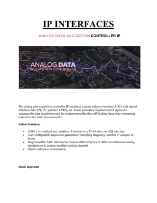
1. IP INTERFACES
ANALOG DATA ACQUISITION CONTROLLER IP
The analog data acquisition controller IP interfaces various industry-standard ADCs with digital
interfaces like SPI, I2
C, parallel, LVDS, etc. It also generates required control signals to
sequence the data acquisition task for a microcontroller thus off-loading these time-consuming
tasks from the host microcontroller.
Salient features:
• AXI4-Lite standard user interface. Connects as a 32-bit slave on AXI interface
• User-configurable acquisition parameters: Sampling frequency, number of samples in
bursts.
• Programmable ADC interface to connect different types of ADCs in addition to analog
multiplexers to connect multiple analog channels
• Optimized power consumption
Block diagram:
2. Applications:
• In conventional FPGAs require an external ADC to convert multiple analog signals into
digital values for real-time processing.
• Sensor node with multiple analog sensors.
MULTI-PROTOCOL SYNCHRONOUS SERIAL ENGINE IP
The Multi-Protocol Synchronous Serial Engine IP integrates basic serial interface
protocols like UART, SPI, and I2C into a single AXI interface port. The individual
modules for these protocols have been implemented in a ruggedized form to avoid bus
errors due to interfering noise from various sources thus making it suitable for application
in automobile electronics.
3. Salient features:
• AXI4-Lite standard user interface. Connects as a 32-bit slave on AXI interface
• Ruggedized SPI, I2C, and UART interface
• User-configurable number and type of interfaces through a configuration tool
• User-configurable parameters of each interface like baud rate/ datarate, modes, length of
transmission, etc.
• Supports master and slave modes for SPI and I2C interfaces
• Configurable number of slaves on SPI interface
• Contains hardware FIFO for UART, SPI, and I2C interfaces with configurable depth up
to 1024 words
Block diagram:
Applications:
4. • Sensor interfaces with SPI and I2C protocol.
• UART interfaces for data transmission between nodes.
18-BIT PIPELINE DSP SLICE IP CORE
The 18-bit Pipeline DSP slice IP Core provides the best utilization of device resources like
memory, I/O, processor, and clock. It is based on the pipelining technique which uses
instruction-level parallelism within a single processor. It supports many independent functions,
including multiplier, multiplier accumulator (MAC), multiplier-adder, higher bit adder, 3-input
adder, barrel shifter, wide bus multiplexers, magnitude comparator, and counter. It also
supports connecting multiple DSP slices IP Core to form wide math functions, DSP filters, and
complex arithmetic. The architectural highlights of the 18-bit Pipeline DSP slice IP core are as
follows:
5. • 18-bit by 18-bit, two's-complement multiplier with the 36-bit result, sign-extended to 48
bits
• Three-input, flexible 48-bit adder/subtractor with optional feedback of accumulator
register.
• Dynamic user-controlled operation select pins to adapt according to single/multiple slice
functions from clock cycle to clock cycle
• Cascading of 18-bit input bus and 48-bit output bus using
INTERCONIN/INTERCONOUT pins supporting propagation of partial products from
one slice to another.
• Multi-precision multiplier and arithmetic support right shifting by 17 bits to obtain wide
multiplier partial products
• Symmetric rounding and sequential/parallel support for greater computational accuracy
• Multi-level pipelining options for control and data signals to improve throughput
• MFC(Multi-Functional C-input) supports multiply-add operation, three-input addition,
and rounding mode
• Separate reset and clock enable for control and data registers, I/O registers, ensuring
maximum clock performance
IMPROVED ADC IP
Flash ADCs are one of the fastest ADCs available which can achieve Giga samples per second
conversion rates. One of the limitations of this ADC type is that their architectural complexity
increases exponentially with an increase in the bit resolution. Hence these are generally available
up-to 8-bit resolutions. On the contrary, other ADC architectures are slow sampling and are
available with high bit resolutions viz. 16-22 bit resolutions. It would be desirable to combine the
fast conversion speeds of flash ADCs with high resolutions of SAR and Σ-Δ ADCs.
The Improved ADC IP provides an interface with a flash ADC and supporting components in
implementing a multi-step ADC to achieve higher bit resolutions thus integrating the speed of
the flash ADC with the resolution of SAR ADC. The controller module in the IP generates all the
necessary signals for the ADC and the supporting components to operate in unison. It can be
used to double the resolution in bits for any ADC in consideration.
6. Salient features:
• The AXI4-Lite standard interface connects as a 32-bit slave on the AXI interface bus.
• Doubles the nominal flash ADC resolution
• Programmable sampling rates and ADC interface types to connect multiple types of
ADCs and DACs
Application:
• High-resolution requirement analog signals from sensors.
Block Diagram:
7. AXI-USB 2.0 DEVICE IP
USB is a generic interface in the modern days to connect to various high-speed data peripherals.
Many USB device/client controllers are introduced in the embedded systems market, which
enables interfacing a host microcontroller to quickly and easily connect to a USB host such as a
PC or industrial PC. One of the major limitations of these controllers is the bottleneck on data
rate imposed by the interface between the host microcontroller and the USB device controller
which more often is a serial UART interface, SPI interface, JTAG interface, or FIFO interface.
In FPGA based embedded systems with reconfiguration capability, it is desirable to implement
this USB controller on-chip and thus implement an SoC. Our AXI-USB 2.0 Device IP supports
high speed, high bandwidth isochronous transactions.
We present an AXI-USB 2.0 Device IP to implement on an FPGA in an embedded system. It
carries out all tasks like USB device enumeration, endpoint instantiations, etc., and enables bulk,
isochronous, interrupts, and control packet transfers over USB. With the addition of a low-cost
external USB PHY chip, a USB device can be realized using this IP in no time. The user
interface to the host microcontroller instantiated on the FPGA is provided in an AXI interface
format and thus, the USB controller is made as a memory-mapped device accessible from the
industry-standard AXI bus from the host microcontroller.
Salient features:
• AXI4-Lite standard user interface. Connects as a 32-bit slave on AXI interface
• USB serial interface engine implemented to support USB2.0 full speed and high-speed
interface
• Supports ULPI interface to external PHY chip
• Supports control, bulk, interrupt, and isochronous transfers on USB interface
8. • 8 endpoints instantiated with endpoint 0 as the control endpoint
• Handles USB enumeration process
EXTERNAL FLASH MEMORY INTERFACE IP
Flash memory forms a basic constituent in many FPGA based embedded systems using Xilinx
SRAM based FPGAs. This is primarily because they store the bitstream file for the FPGA using
which the FPGA configures itself at every startup. After configuration, the flash memory is
available for user data storage and can be used for non-volatile data storage as long as it is
outside of the bitstream area. The External Flash Memory Interface IP designed atFastream
Technologies allows accessing these memory locations as a memory-mapped interface and
makes the controller agnostic of the underlying SPI interface on which the memory is being
interfaced.
Salient features:
• AXI4-Lite standard user interface. Connects as a 32-bit slave on AXI interface
• Page-wise programming according to the flash memory requirements handled by the IP
• Memory single bit error detection and correction implemented in the IP-core.
• User-configurable, industry-standard NOR flash memories can be interfaced with the IP
on SPI and Quad-SPI interfaces.
Block diagram:
9. PRECISION TIME PROTOCOL IP
Time synchronization is of prime importance in distributed industrial control systems and in
automotive networks. The timestamps of events in a distributed control system should match
with considerable accuracy to be able to correlate them together or for the control system to
operate properly. Various time synchronization protocols are used on different networks which
allow synchronization up to various accuracies. Precision Time Protocol or PTP or IEEE1588 is
one such protocol that allows synchronization of an order of 1us with the master (most accurate)
clock in the network. On local area Ethernet networks, it is implemented in various ways most
often in software. This method is inherently less accurate for timestamping which results in a
reduction of synchronization accuracy. Implementing a time stamp unit in hardware that
generates time stamps as soon as the PTP packet arrives from the network allows more accurate
time stamps and hence, better synchronization. The precision time protocol IP designed at
Faststream technologies implements the PTP on Ethernet networks and sends the packet to the
MAC. A precise time stamping unit instantiated in the IP captures the time stamp as soon as the
packet is received and decoded. The values of offset and delay required to correct the local slave
clock are generated by the IP.
10. Salient features:
• AXI4-Lite standard user interface. Connects as a 32-bit slave on AXI interface
• Identifies PTP packets like sync, follow-up, and delay-response and sends delay-request
packets.
• PPS clock output
• Offset and drift adjustable clock internally used
Block diagram:
11. DELAY LOCKED LOOP IP
Generation of the clock signal with a fixed but programmable phase difference with respect to a
reference input clock is critical in many applications. An all-digital DLL design with several
features like a wide lock range for input frequencies, short locking time, and reduced jitter is
achieved by this IP. The all-digital nature of the DLL design allows the addition of clocking
resources in FPGA prototyping of new IPs and for FPGA-based embedded systems using
multiple clocking resources. Rigorous simulation has been carried out to evaluate the robustness
and performance of the IP. The Delay Locked Loop IP can be used for a variety of applications
that require precise phase shifts with respect to reference clocks to adjust for the channel routing
delays on the PCB.
Applications:
• BIST circuits for measurement of setup and hold times
• Phase detection and tracking
• Clock recovery from the input data stream
• High-speed DDR type interface applications to align data with clock edges
Salient features:
12. • Timing resolution: 80ps
• Operating frequency range: 160MHz - 700 MHz
• Lock time: 11 cycles
• Generates user-configurable precise phase shifts from 00 to 3600 with a resolution of 10
• Delays multiple periodic or aperiodic signals independent of voltage and temperature.
Block diagram: