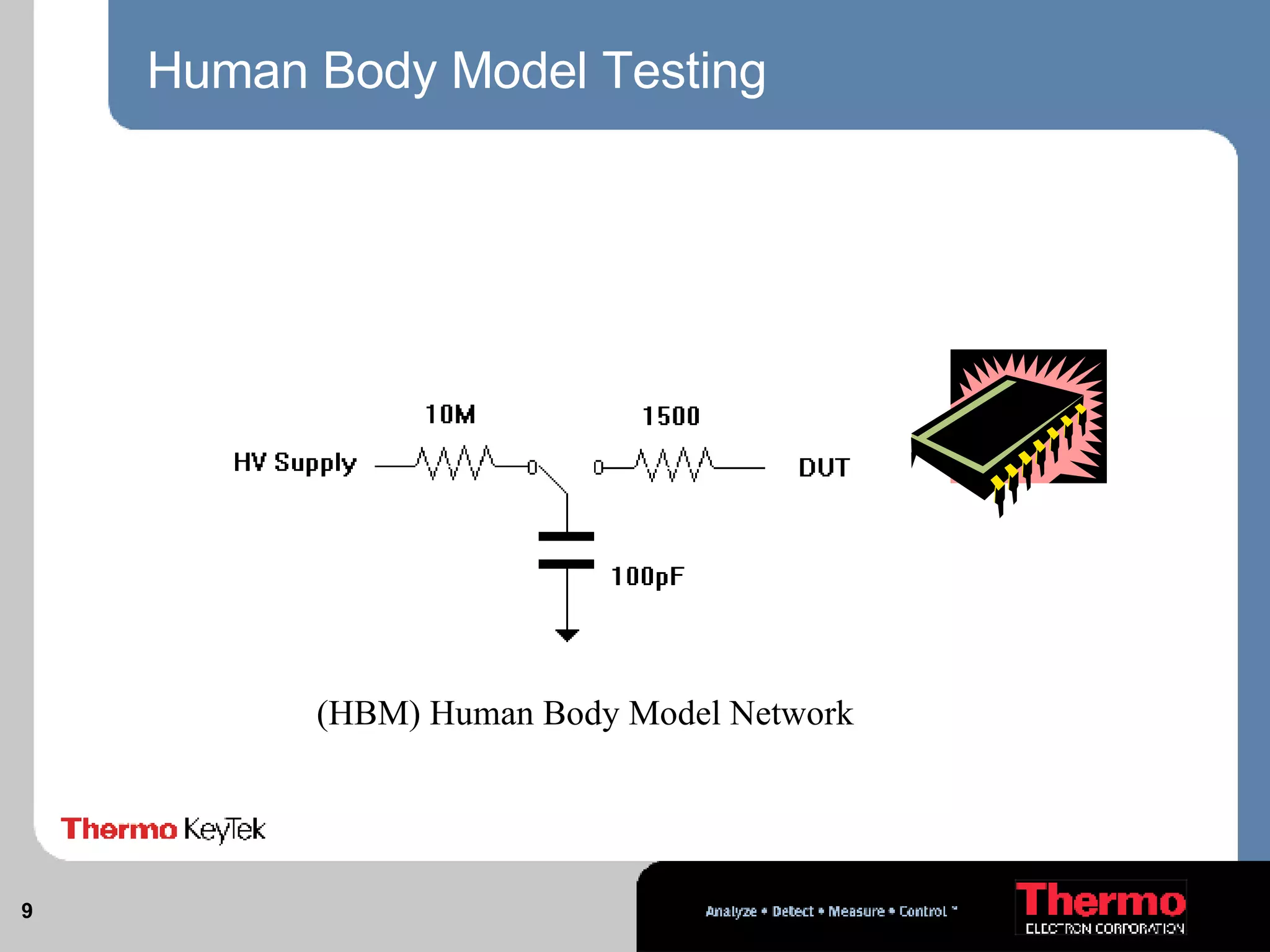
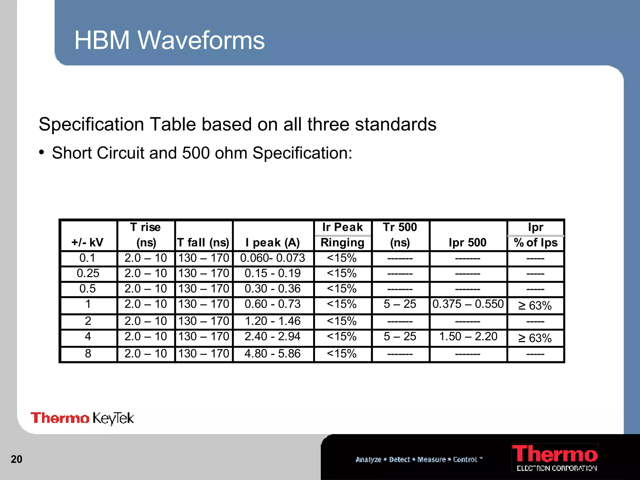
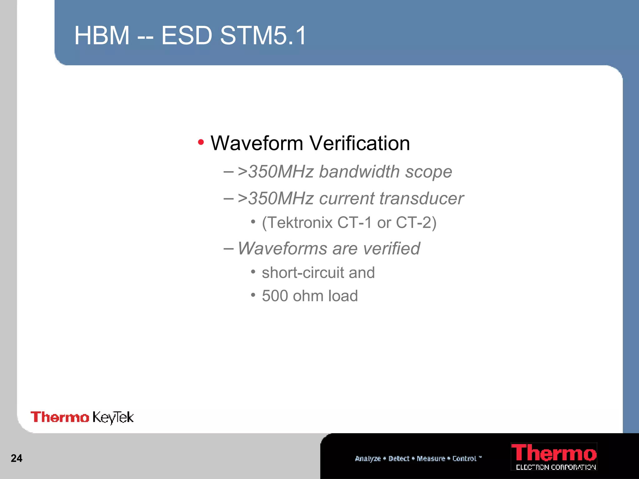
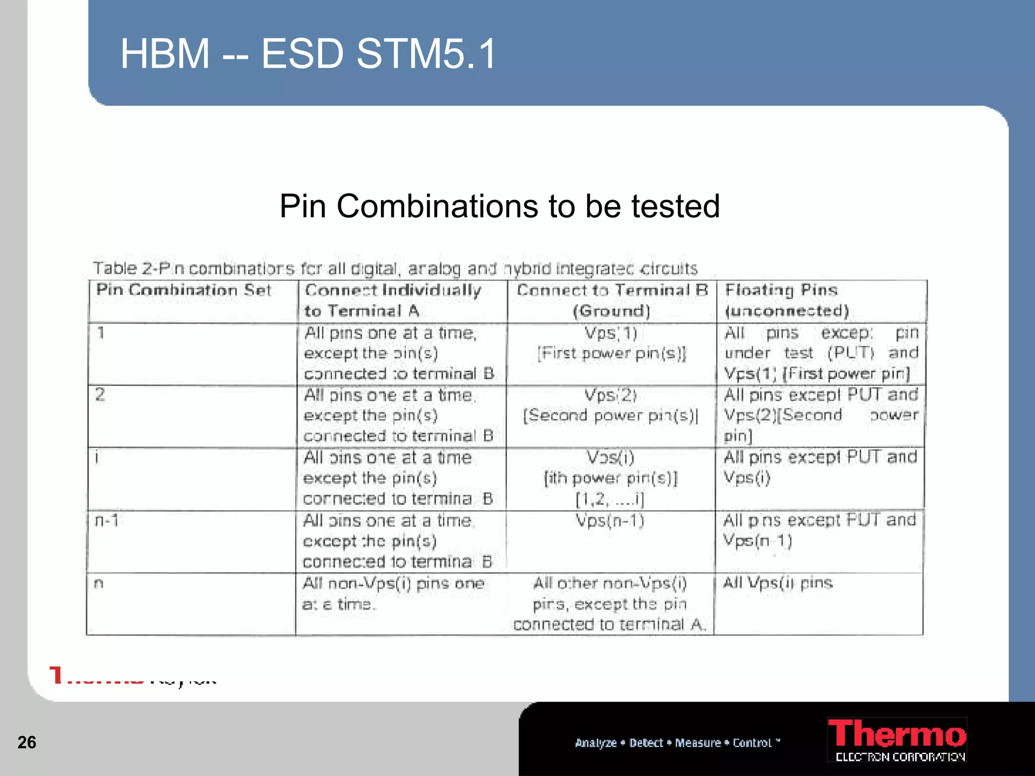
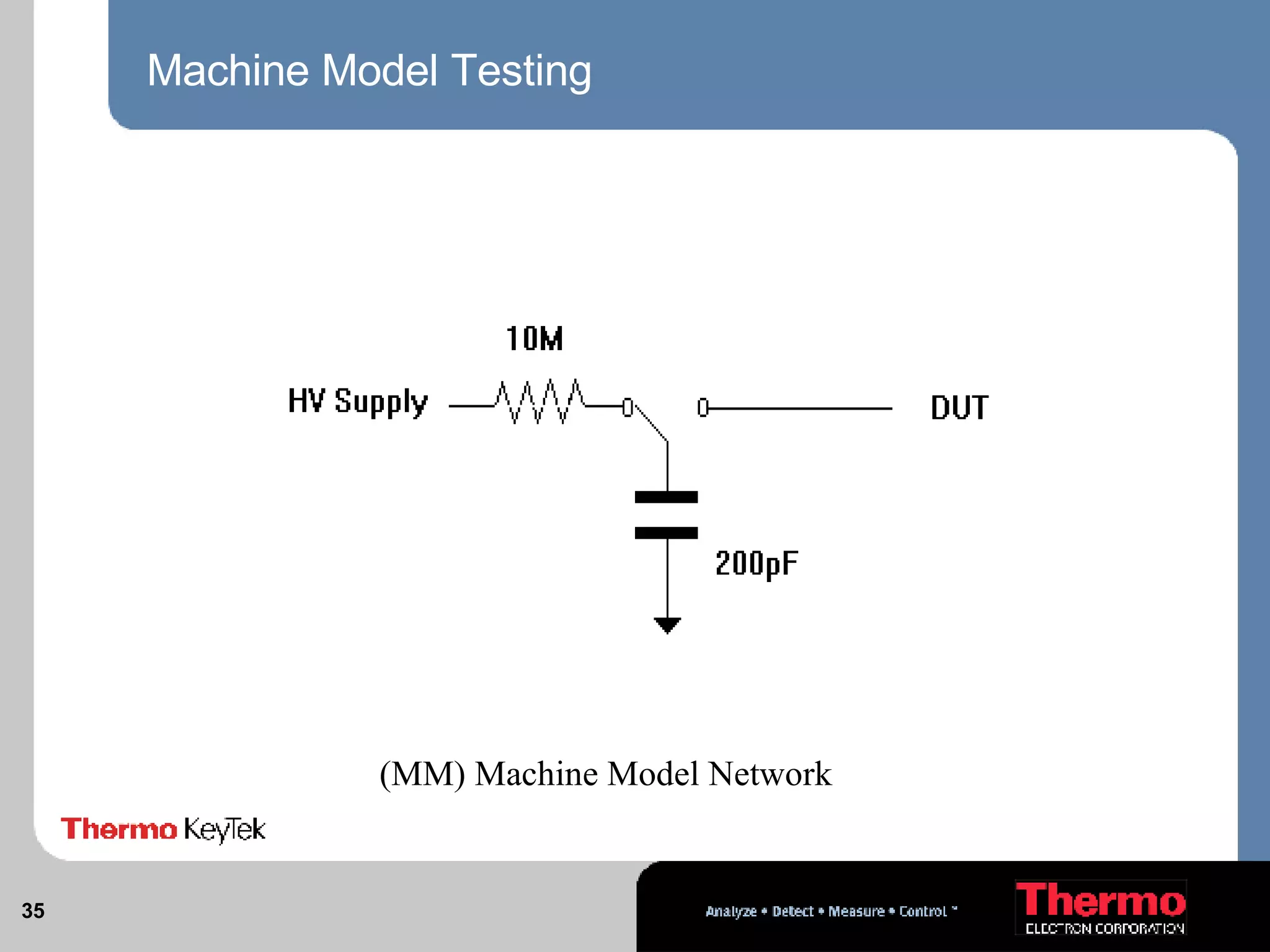
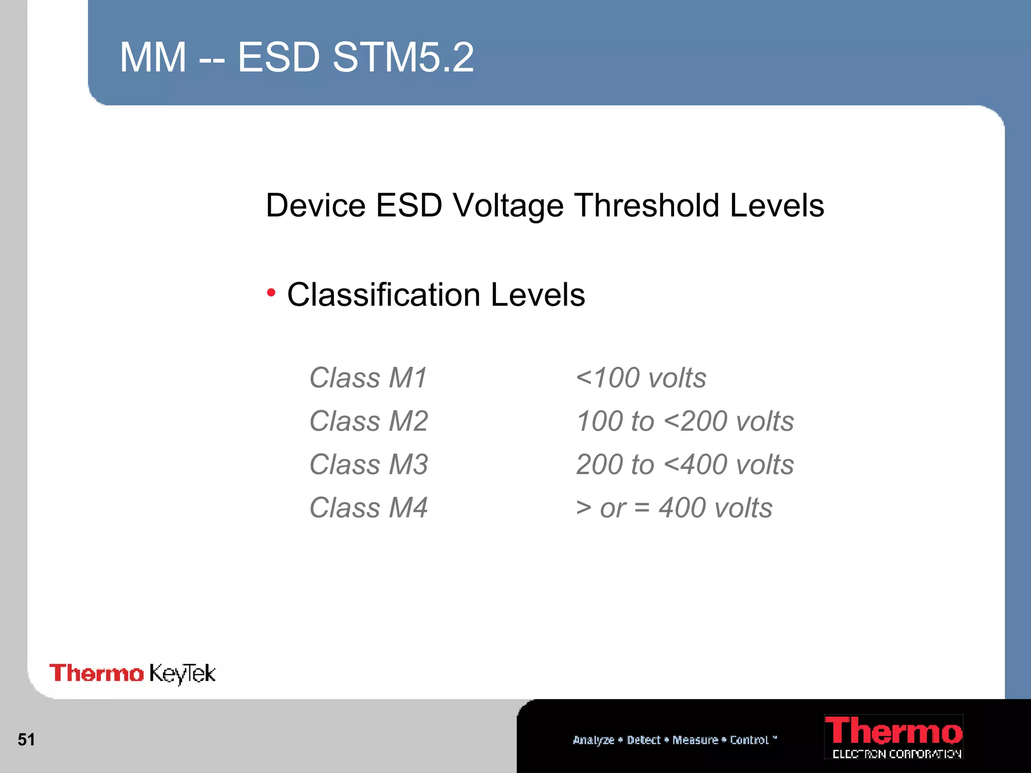
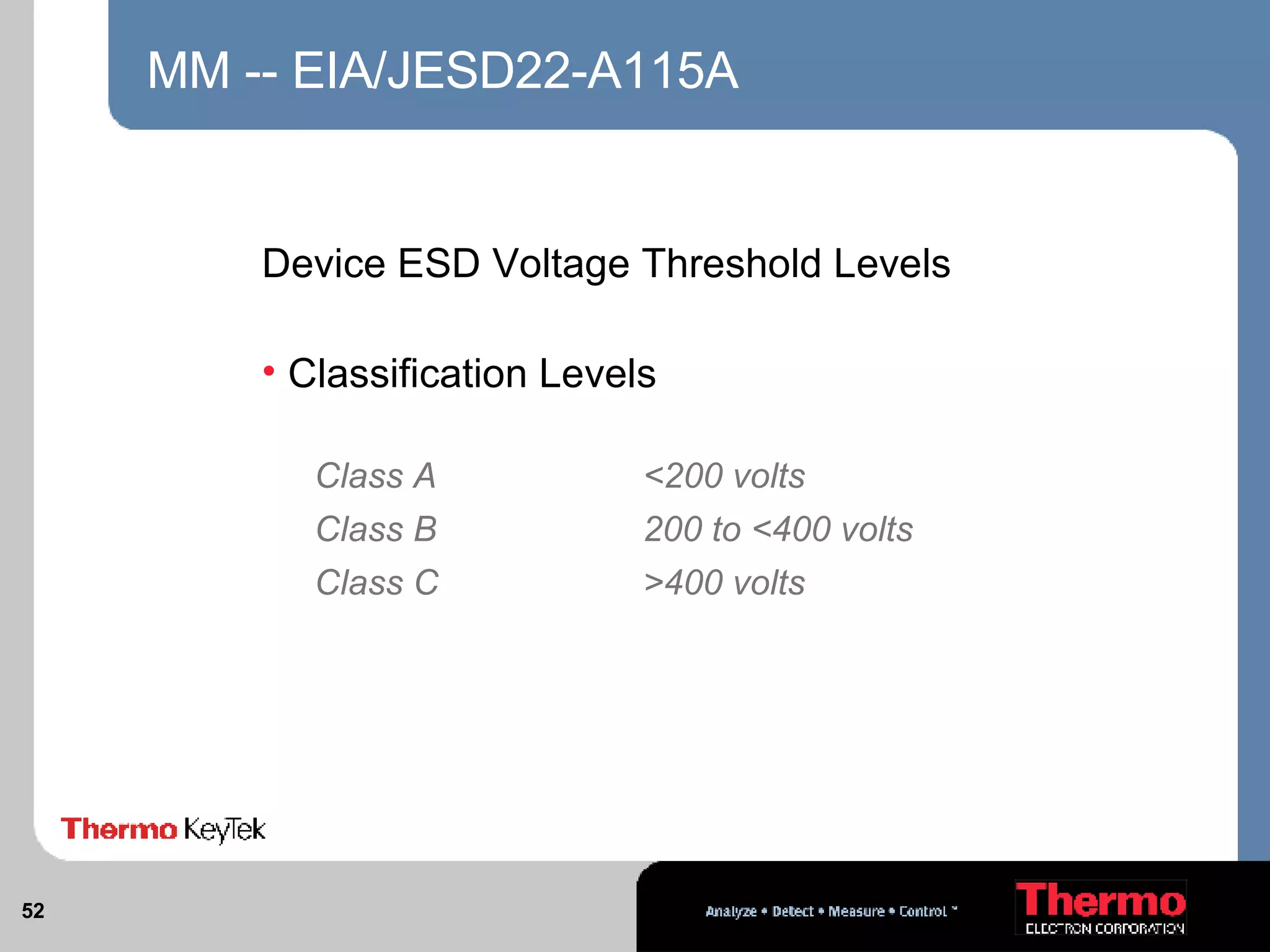
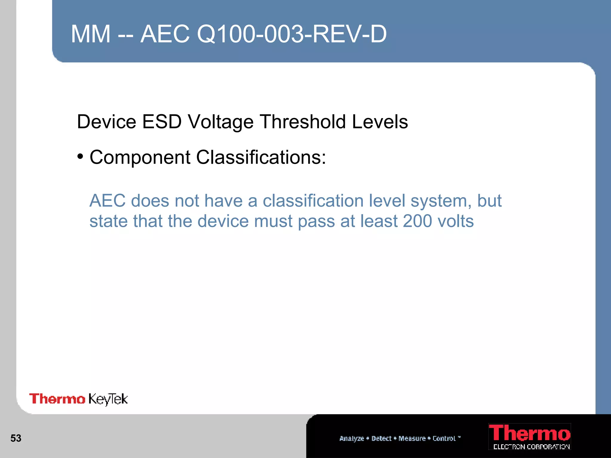
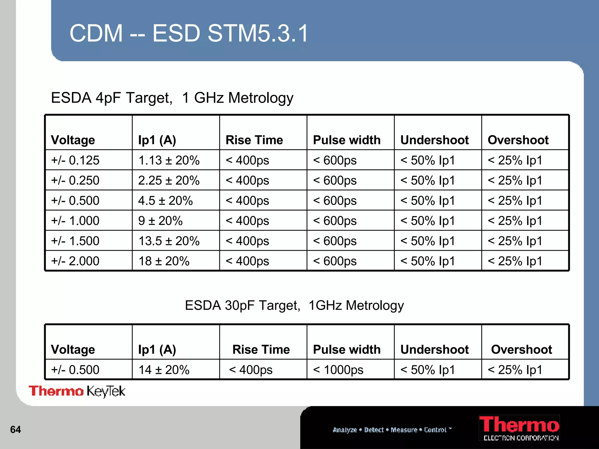
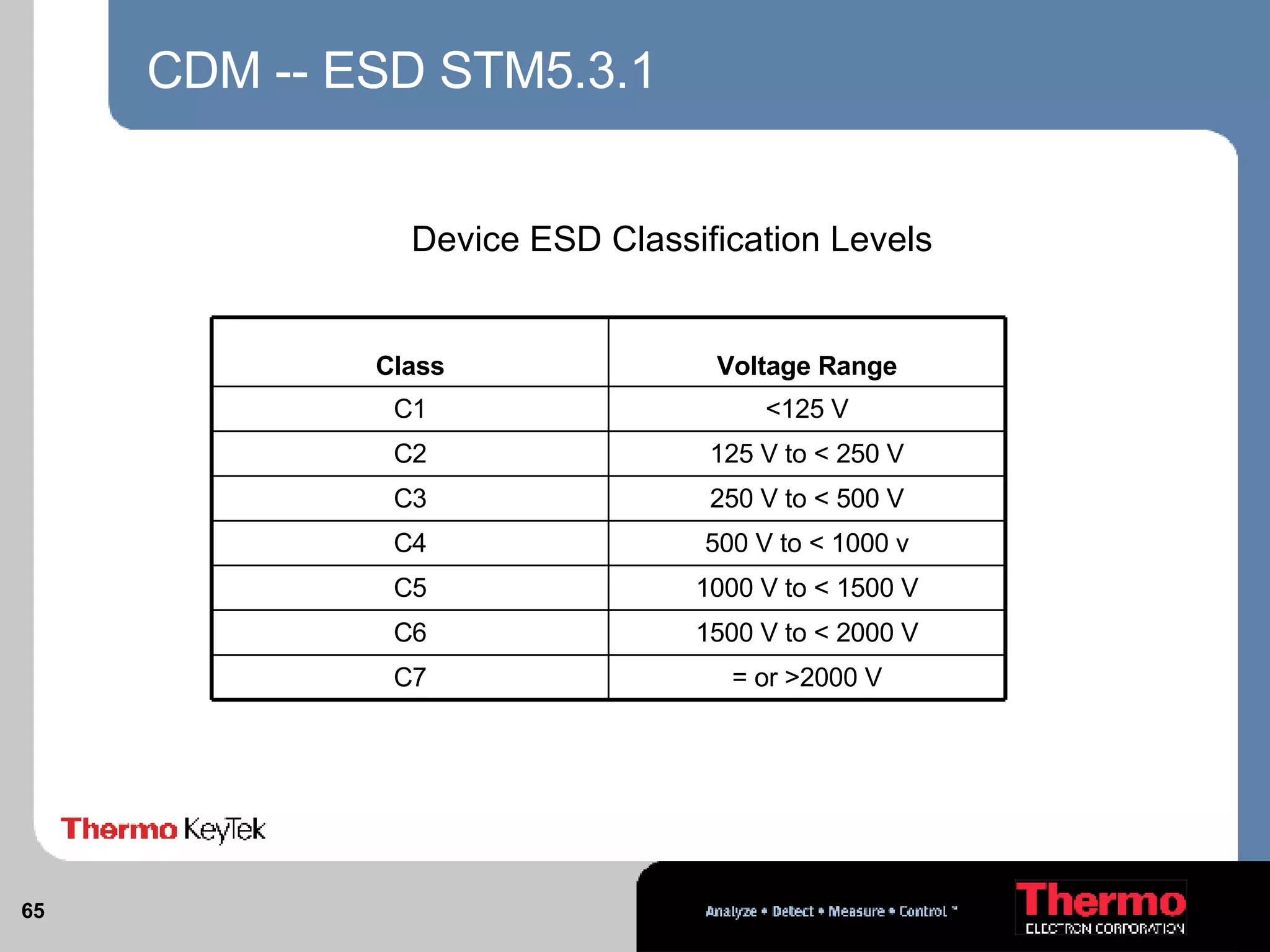
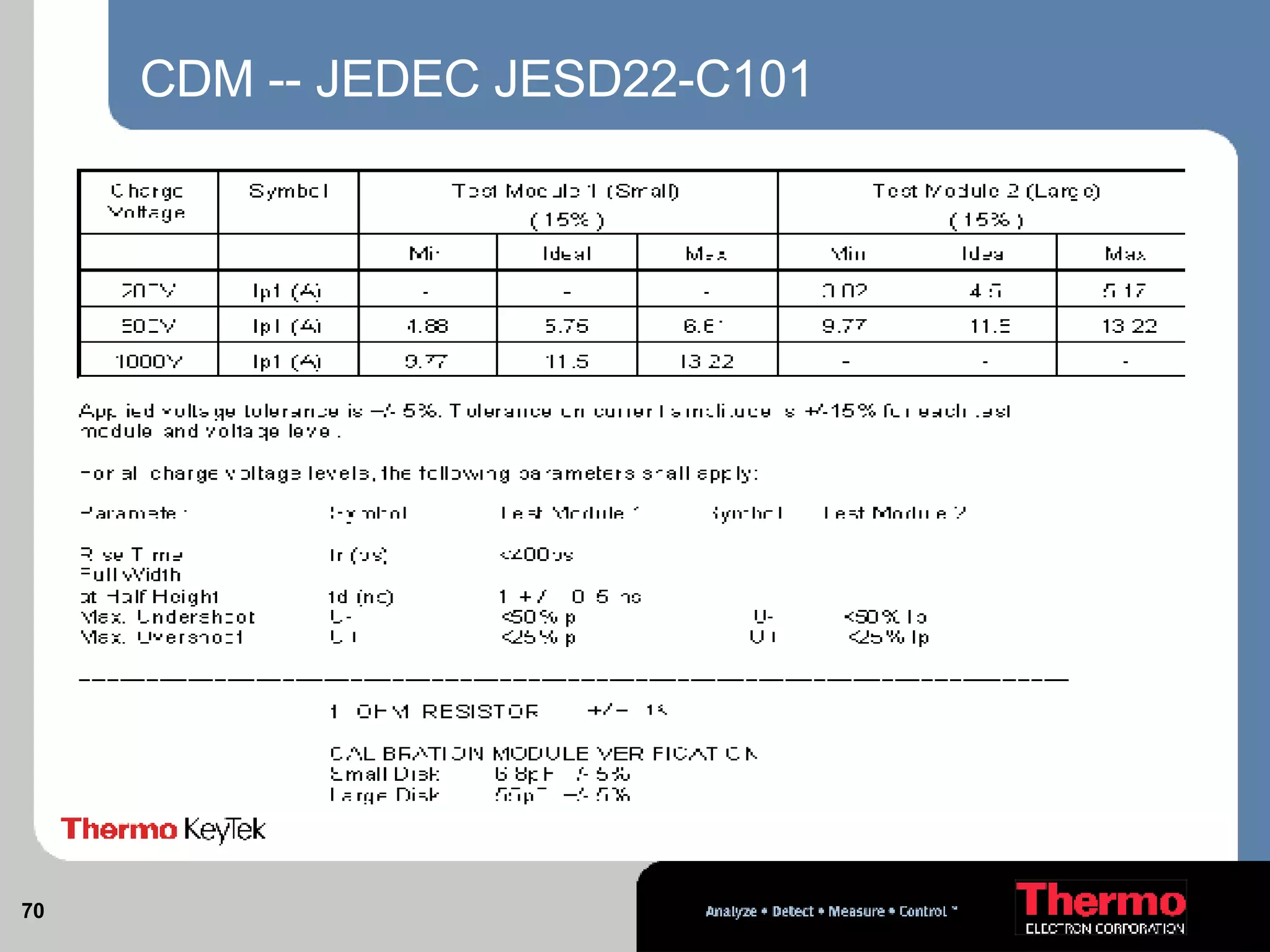
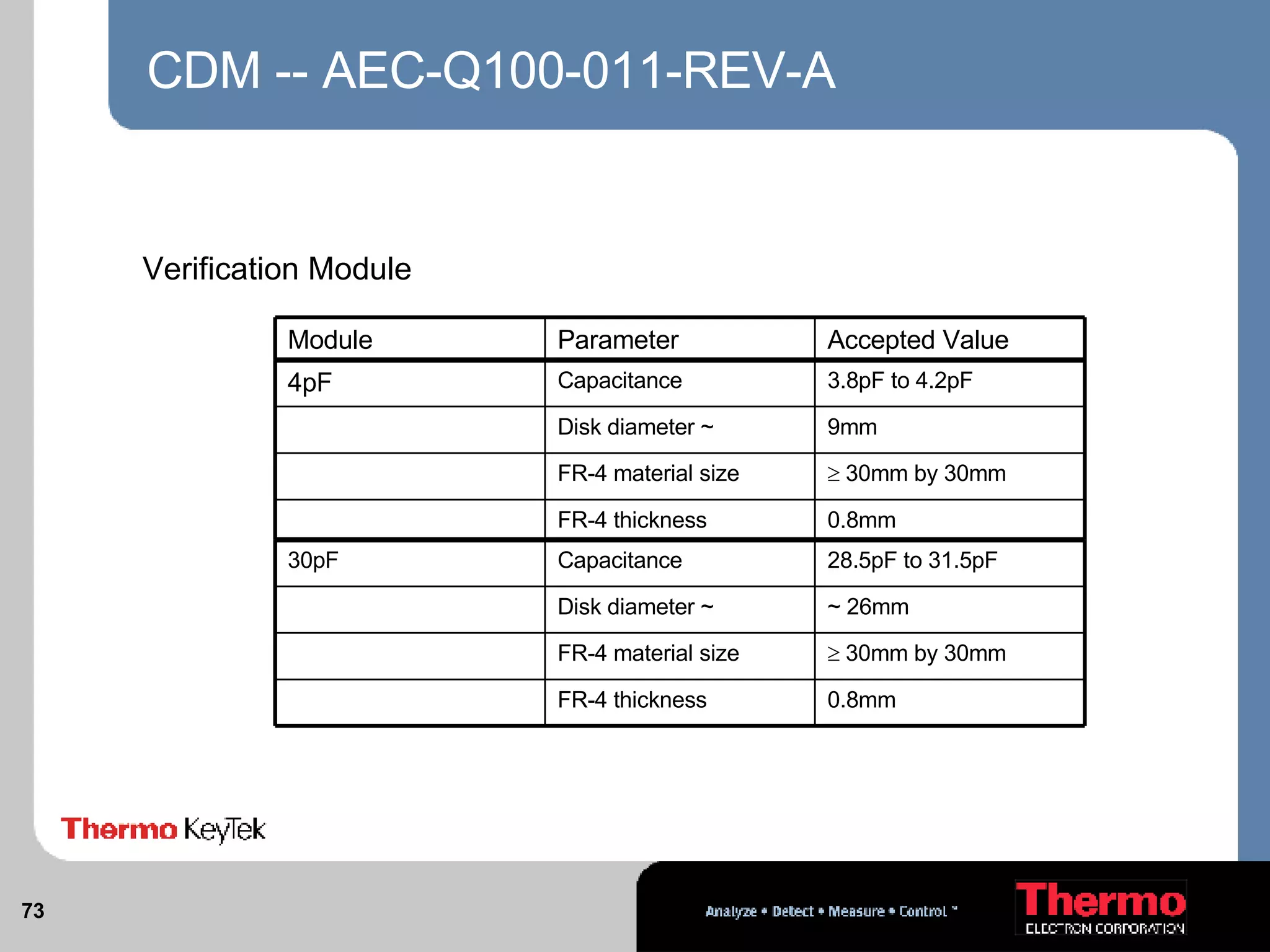
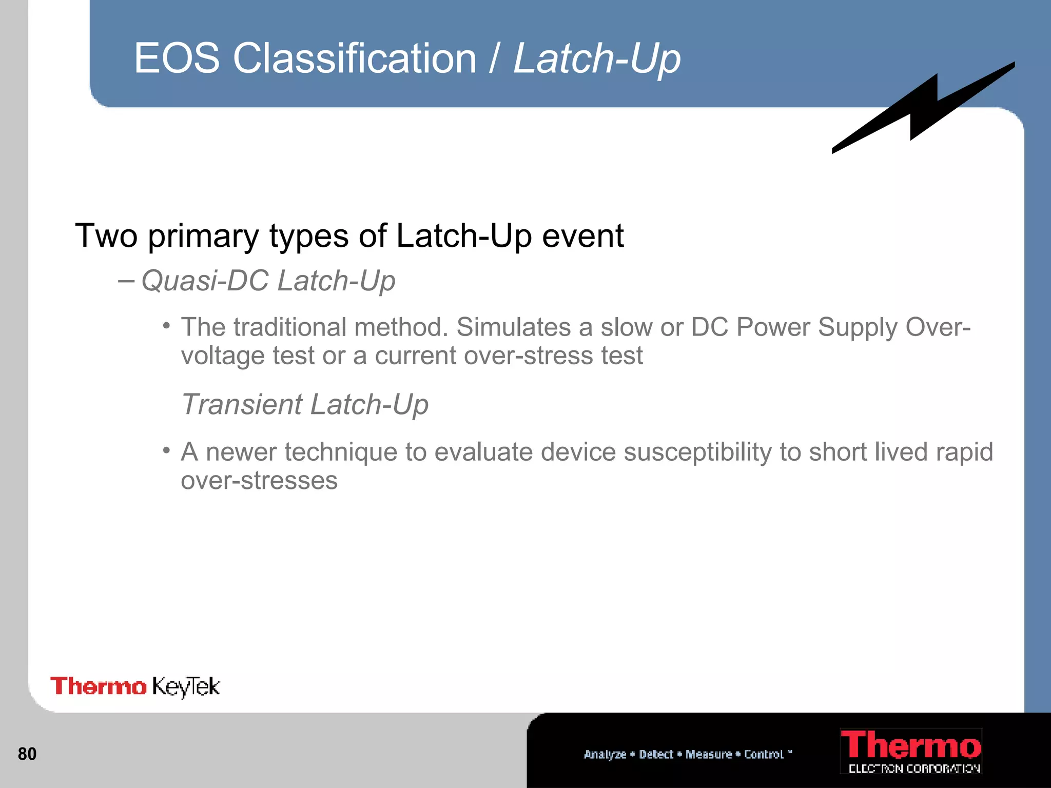
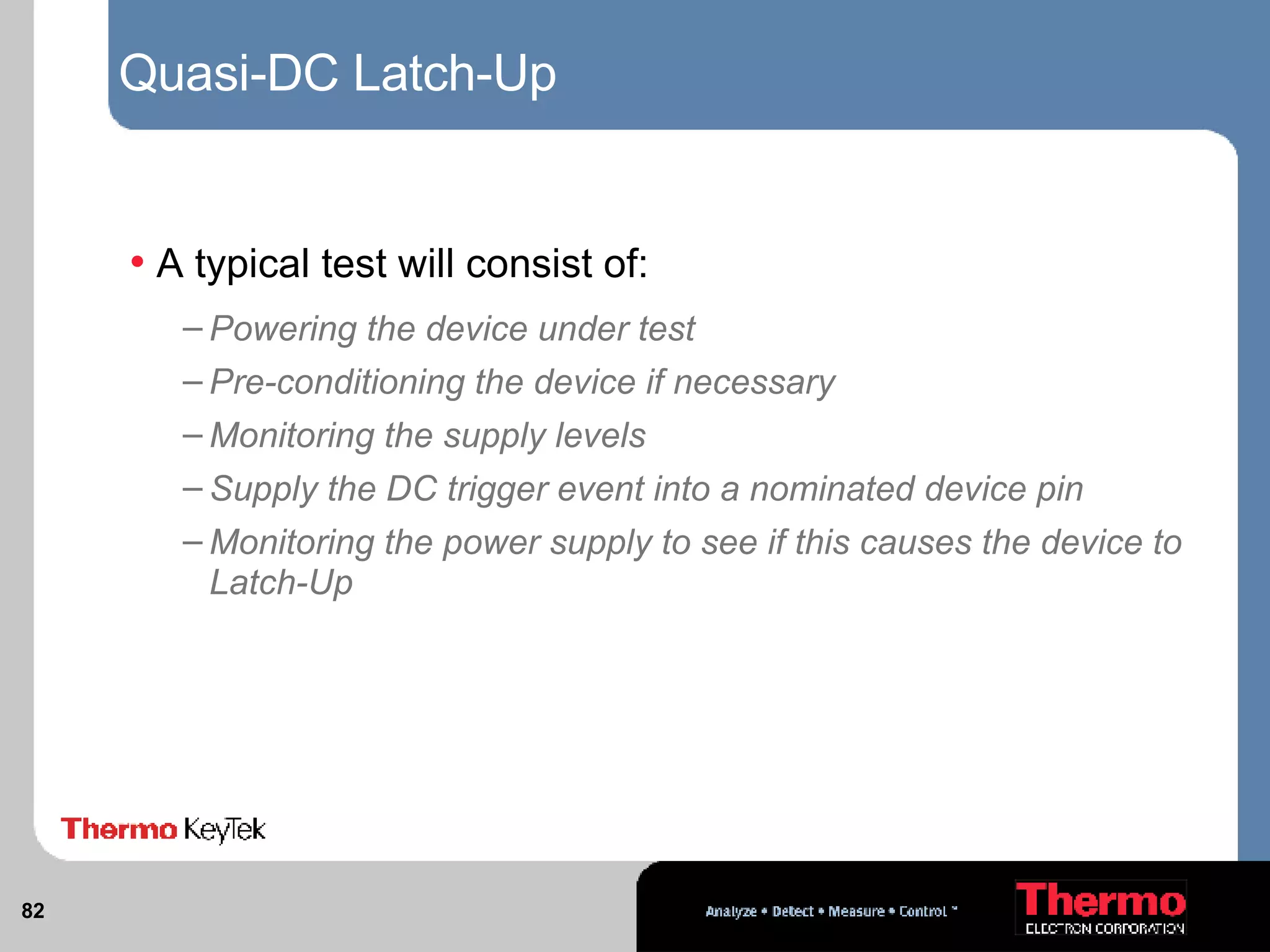
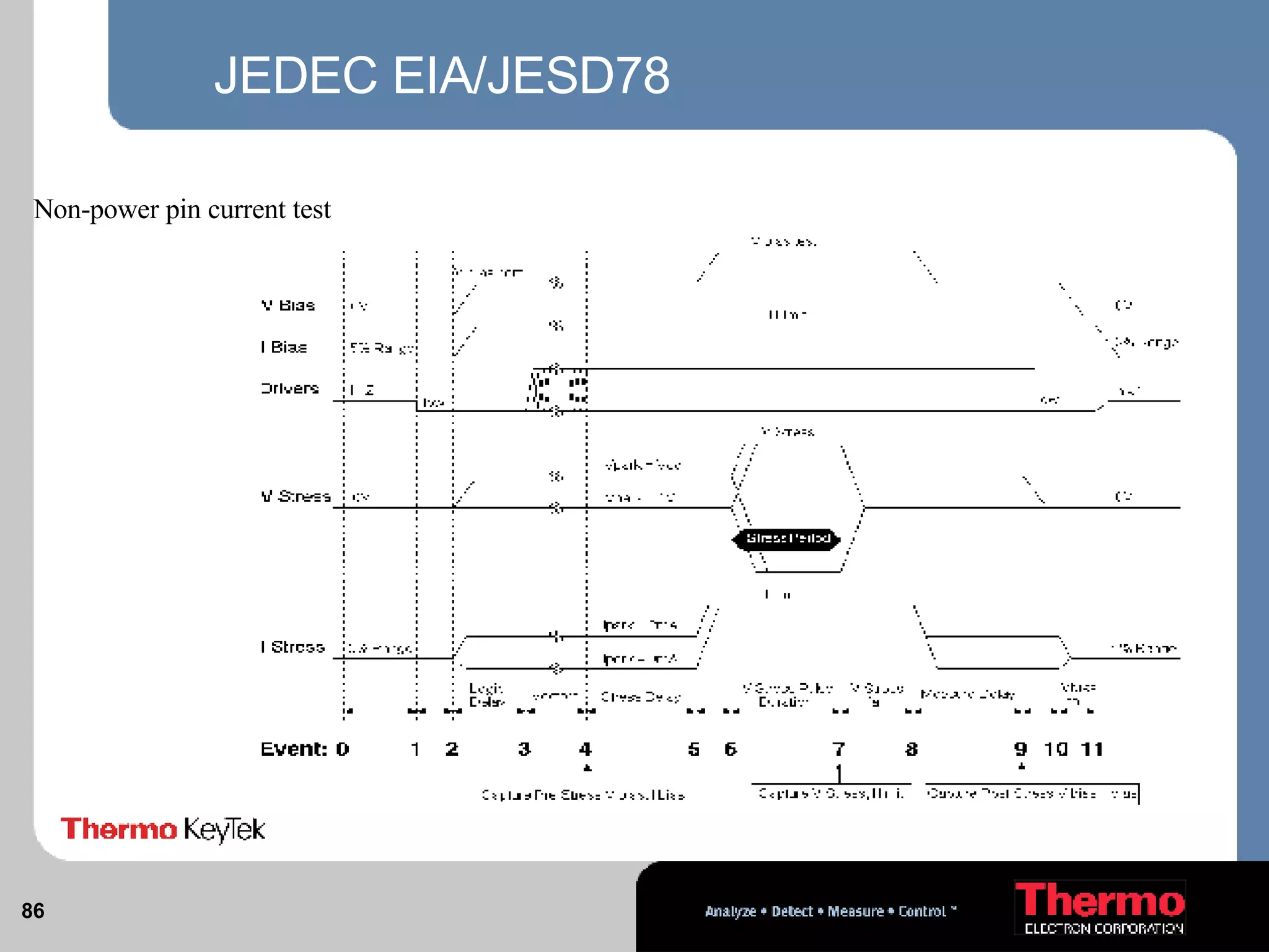
EOS/ESD Testing Today 訊程實業 (Kimpsion Corp.)  www .Kimpsion .com E-mail: PaulH@Kimpsion.com
ESD -  E lectro- S tatic  D ischarge “ Equalization of different electrostatic potentials between two or more objects” EOS -  E lectrical  O ver- S tress “ An electrical event that is outside the specified range of the device under test”  (Latch-up) EOS or ESD   ?
Both will damage devices by a rapid localized heating of the semiconductor material or by rapidly creating strong electrical fields Critically, even very small discharges or over-stress can be fatal or cause latent failures EOS or ESD !
Dominant ESD Test Methods (HBM) Human Body Model (MM) Machine Model (CDM) Charged Device Model Non-socketed (SDM) Socketed Device Model Socketed CDM  HBM testing is the principle test requirement for industry.  CDM is today recognised as a high priority for implementation.
EOS/ESD Seminar Topics HBM (Human Body Model) Test Requirements MIL-STD  ESDA  JEDEC  AEC MM (Machine Model) Test Requirements ESDA JEDEC AEC  CDM (Charged Device Model) Test Requirements Robotic CDM – ESDA / JEDEC / AEC Socketed CDM - ESDA
EOS/ESD Seminar Topics (continued) Quasi DC Static Latch-up testing JEDEC, JESD 17-1988 (OBSOLETE) JEDEC EIA/JESD78  Automotive Electronics Council AEC-Q100-004-REV-D Transient Induced Latch-up ESD Association WG5.4 (work in progress) Internal standards of major companies
ESD Classifications - - HBM EOS/ESD Seminar
ESD Classifications - - HBM HBM - Human Body Model Primary Standards US MIL-STD-883E method 3015.7 notice 8  ESD Association STM5.1-2001 JEDEC EIA/JESD22-A114-B Automotive Electronics Council  AEC-Q100-002-REV-D
Human Body Model Testing (HBM) Human Body Model Network
HBM Evolution US MIL-STD-883 was the first standard to define the HBM waveform  ESDA, JEDEC and AEC specifications added a 500 ohm measurement.  This measurement ensures that the overall system stray capacitance, including socket capacitance and capacitance contributed from the fixture are kept within the standards specification. i.e. minimised.
HBM Evolution ESDA STM5.1-2001 and EIA/JESD22-A114-B are now considered to be the industry standard test methods for HBM.  (The AEC standard is based on the JEDEC standard)  The ESD Association, through the ESDA symposium, is responsible for publishing many original research papers and driving the refinement of the MIL-STD-883 standard.
Basic HBM Test Methodologies Each standard defines the relationship between pin groups while performing the actual stressing which pins are stressed (zapped), which pins are grounded, which pins are floating.  These requirements were originally specified in MIL-STD-883 and are still currently referenced by several standards.
Basic HBM Test Methodologies Zap Methods required Zap all pins vs. (n) VSS pin groups at ground (all other pins floating) Zap all pins vs. (n) power pin groups at ground (all other pins floating) (n) is the number of separate power rails Metalized pins should be group together. Non-metalized power pins, must be treated as separate power pin groups, for testing purposes.
Basic HBM Test Methodologies Zap Methods required (continued) Zap each IO pin vs. all other IO pins at ground (all other pins floating) Note: With the requirement to separate non-metalized power pins into multiple groups, the amount of zaps per pins can be greatly increased.  Example: 6 power groups, 1 zap per polarity, 1 zap level.   Therefore each IO pin would receive 14 zaps!
Basic HBM Test Methodologies Zap Method requirements n positive / n negative zaps at each voltage level MIL-STD - 3 zaps per polarity ESDA - 1 zap per polarity  JEDEC - 1 zap per polarity  AEC - 1 zap per polarity
Basic HBM Test Methodologies Zap Method requirements Time between zaps (Zap Interval)  MIL-Std - 1second between zaps ESDA - 0.3 seconds between zaps JEDEC - 0.3 second between zaps Soon to be 0.1 seconds with pending JESD22-A114-C AEC - 0.5 seconds between zaps
Basic HBM Test Methodologies Classification Testing  A minimum of 3 devices is the specified sample lot To avoid over-stressing a device, some companies will use separate devices for each zap method when testing devices with multiple power and ground pin groups They may also use individual devices for for each different voltage level
HBM Waveforms Short Circuit Waveform 1 kV = 0.67A +/- 10% CT1 and 20dB attenuator 0.5V /A Rise Time Measurement  10 to 90% 2 - 10nS
HBM Waveforms 500 ohm waveform   1kV = 0.375 – 0.550A 4kV = 1.50 – 2.20A ≥  63%   CT1 and 20dB attenuator 0.5V /A
HBM Waveforms Specification Table based on all three standards Short Circuit and 500 ohm Specification:
HBM -- MIL-STD-883E History Developed as the industries first device level ESD test method Waveform definition was changed from the original voltage waveform to today’s current waveform, in one of it’s updates  Note: The military now accepts ESD STM5.1 in place of MIL-STD 883E
HBM -- MIL-STD 883E Any semiconductor used in the U.S. Military Industrial Complex must meet the requirements of MIL-STD-883E In other words: Any product used in military or military associated applications must use semiconductors that have been qualified and listed to have a specific ESD withstand level.
HBM -- MIL-STD 883E Device ESD Voltage Threshold Levels  Classification Levels Class 1 0 to 1,999 volts  Class 2 2000 to 3,999 volts Class 3  4,000 volts and above
HBM -- ESD STM5.1 Waveform Verification >350MHz bandwidth scope >350MHz current transducer  (Tektronix CT-1 or CT-2) Waveforms are verified short-circuit and 500 ohm load
HBM -- ESD STM5.1 Daily system verification Verify electrical continuity for all pins Check WCP waveforms at +/-1 and 4kV  (or the stress level to be used). Verify at *kV if stressing above 4kV is required.   Low side of tester to pin with the shortest path High side to each of the other pins, one at a time WCP = Worst Case Pin
HBM -- ESD STM5.1 Pin Combinations to be tested
HBM -- ESD STM5.1 Device ESD Voltage Threshold Levels  Component Classifications: Class 0   <250V 1A 250 to <500V 1B 500 to <1000V 1C 1000 to <2000V 2 2000 to <4000V 3A 4000 to <8000V 3B > or = 8000V
JEDEC History Today, the JEDEC Solid State Technology Association, under the EIA, is responsible for developing standards for all aspects of the semiconductor industry.
JEDEC and ESDA Co-operation JEDEC and the ESDA are attempting to work together, to try and harmonize standards for ESD testing. If they can succeed, there will be a tremendous savings to industry, by eliminating conflicting test methods and the requirement for multiple testing to the different methods.
Device ESD Voltage Threshold Levels  Component Classifications: Class 0   <250V 1A 250 to <500V 1B 500 to <1000V 1C 1000 to <2000V 2 2000 to <4000V 3A 4000 to <8000V 3B > or = 8000V HBM -- JEDEC EIA/JESD22-A114-B
AEC History AEC is the Automotive Electronics Council Responsible for standards used throughout the automotive industry Semiconductors Electrical components Electronic Modules Council was developed, so the automotive manufacturers could control their testing requirements
Device ESD Voltage Threshold Levels  Component Classifications: AEC does not have a classification level system, but state that the device must pass at least 2000 volts HBM – AEC Q100-001-REV C
ESD Classifications - - MM EOS/ESD Seminar
ESD Classifications - - MM  MM - Machine Model Primary Standards ESD Association STM5.2-1999  JEDEC EIA/JESD22-A115A Automotive Electronics Council AEC-Q100-003-REV-D
Machine Model Testing   (MM) Machine Model Network
MM History The original Japanese (EIA/J) standard was meant to represent a worst case human body discharge (HBM), but the standard became known as the Machine Model event.
MM History Other methods were developed, to further refine the EIA/J method and to eliminate flaws in the original method.  Only the storage capacitance and output R remained !
MM Future? Primarily used by the automotive industry, but as the latest release of the AEC Q100 document states, they have indicated that suppliers with CDM capability can provide CDM data instead of MM testing.   (AEC Q100 has also adopted a CDM test method.) Other companies who perform MM testing for the automotive industry may also eliminate MM testing Because of this, the MM test requirements may be replaced by CDM in the future.  Both JEDEC and ESDA have put these committees into Hybernation.
Basic MM Test Methodologies Each standard defines the relationship between pin groups while performing the actual stressing which pins are zapped which pins are grounded which pins are floating.  These requirements were originally specified in the HBM standards
Basic MM Test Methodologies Zap Methods required Zap all pins vs. (n) VSS pin group at ground (all other pins floating) Zap all pins vs. (n) power pin group at ground (all other pins floating) (n) is the number of separate power rails Metalized pins should be group together. Non-metalized power pins, must be treated as separate power pin groups, for testing purposes.
Basic MM Test Methodologies Zap Methods required (continued) Zap each IO pin vs. all other IO pins at ground (all other pins floating) Note: With the requirement to separate non-metalized power pins into multiple groups, the amount of zaps per pins can be greatly increased.  Example: 6 power groups, 1 zap per polarity, 1 zap level, therefore IO pins would receive 14 zaps
Basic MM Test Methodologies Zap Methods’ requirements n positive / n negative polarity zaps at each voltage level ESDA:  n = 3 zap per polarity  JEDEC:  n = 1 zap per polarity  AEC:  n = 1 zap per polarity
Basic MM Test Methodologies Zap Methods’ requirements Time between zaps (Zap Interval)  ESDA:  1 second between zaps JEDEC:  0.5 second between zaps AEC:  1 second between zaps
Basic MM Test Methodologies A minimum of 3 devices is the specified sample lot. To avoid excessive over-stressing, some companies use separate devices for each zap method when testing devices with multiple power and ground pin groups. They may also use individual devices for for each different voltage level.
MM Waveforms Short Circuit Waveform Ip1 = 7A +/- 10% at 400V Ip2 = 67 – 90% of Ip1 Frequency 11-16MHz Period 66 – 90nS
MM Waveforms Specification Table based on all three standards Short Circuit Specification:
MM Waveforms 500 ohm Waveform ESDA  Ipr = 0.85 – 1.2A I 100  =  0.26 – 0.32A JEDEC Ip = I 100  X 4.5 Max I 100  =  0.232 - 0.348
MM Waveforms Specification Table based on all three standards 500 ohm Specification:
MM -- ESD STM5.2 Initial tester and test fixture qualification Verify electrical continuity for all pins Check waveforms at +/-100, 200 and 400V Low side of tester to pin with the shortest path High side to each of the other pins, one at a time. Check waveforms into a 500 ohm load at 400V Same connections as for the short-circuit test
MM -- ESD STM5.2 Daily system verification Verify electrical continuity for all pins Check WCP waveforms at +/- 400V Low side of tester to pin with the shortest path High side to each of the other pins, one at a time WCP = Worst Case Pin
MM -- ESD STM5.2 Device ESD Voltage Threshold Levels  Classification Levels Class M1 <100 volts   Class M2 100 to <200 volts Class M3  200 to <400 volts Class M4 > or = 400 volts
MM -- EIA/JESD22-A115A Device ESD Voltage Threshold Levels  Classification Levels Class A <200 volts   Class B 200 to <400 volts Class C  >400 volts
MM -- AEC Q100-003-REV-D Device ESD Voltage Threshold Levels  Component Classifications: AEC does not have a classification level system, but state that the device must pass at least 200 volts
ESD Classifications - - CDM EOS/ESD Seminar
ESD Classifications - CDM CDM - Charged Device Model Primary Standards ESD Association STM5.3.1 (non-socketed)  ESD Association DS5.3.2 (socketed)  JEDEC JESD22-C101-B (Field Induced test method only) Automotive Electronics Council  AEC-Q100- 011-REV-B (Field Induced test method only)
ESD Classifications - CDM  There are two major approaches to CDM testing Non-Socketed (Robotic CDM) Field Induced Charge  Direct Charge Socketed (Socketed CDM) There are clear advantages to both methods
CDM approaches  Scientifically pure Replicates real world Unlimited pin count Integrated waveform monitoring Direct charging Field charging Very easy to use Fast set up and changing of devices High throughput Integrated parametric tests for all packages Same test system as your HBM / MM tester
CDM Evolution The original CDM waveform and subsequent test system was developed by AT&T Bell Labs in the US in the mid 80’s.  Their system became know has the “Happy Zap”
CDM Evolution This architecture and waveform was the basis for the development of the JEDEC standard (JEDEC JESD22-C101)  Perceived flaws in the JEDEC standard drove the ESD Assoc. developed their own method.
CDM - Basic Test Methodologies CDM events occur when the package has become charged and it discharges to an object with a lower potential.
CDM Network Models The real series R for CDM is on the order of  10’s of ohms and is predominantly caused by the arc resistance and discharge pin inductance.
CDM - Basic Test Methodologies CDM testers replicate this event by artificially charging the device and grounding the pins to be stressed.
CDM -- ESD STM5.3.1 ESDA CDM Waveform
CDM -- ESD STM5.3.1 ESDA 30pF Target,  1GHz Metrology ESDA 4pF Target,  1 GHz Metrology < 25% Ip1 < 50% Ip1  < 600ps < 400ps 18 ± 20%  +/- 2.000  < 25% Ip1 < 50% Ip1 < 600ps < 400ps 13.5 ± 20% +/- 1.500 < 25% Ip1 < 50% Ip1 < 600ps < 400ps 9 ± 20%  +/- 1.000  < 25% Ip1 < 50% Ip1  < 600ps < 400ps 4.5 ± 20%  +/- 0.500  < 25% Ip1 < 50% Ip1  < 600ps < 400ps 2.25 ± 20%  +/- 0.250  < 25% Ip1  < 50% Ip1  < 600ps  < 400ps  1.13 ± 20%  +/- 0.125  Overshoot   Undershoot Pulse width Rise Time Ip1 (A) Voltage < 25% Ip1 < 50% Ip1 < 1000ps < 400ps 14 ± 20% +/- 0.500  Overshoot   Undershoot Pulse width Rise Time Ip1 (A)   Voltage
CDM -- ESD STM5.3.1 Device ESD Classification Levels = or >2000 V C7 1500 V to < 2000 V C6 1000 V to < 1500 V C5 500 V to < 1000 v C4 250 V to < 500 V C3 125 V to < 250 V C2 <125 V C1 Voltage Range Class
CDM -- ESD STM5.3.1 WIP (Work in Progress) New calibration targets are being evaluated. Possible redesign of the Ground Plane and Charge Plates. Additional high bandwidth calibration procedures are being reviewed, with the possible elimination of the 3.5GHz scope requirement. Overall calibration chain verification method is being reviewed.
CDM -- JEDEC JESD22-C101-A Changes in the recent releases C101 to C101A Specification of the dielectric thickness was added to the standard (KeyTek discovered that the thickness has to 15mil’s to achieve the required waveforms) The waveform Ip specification was changed to conform to that obtained by installed, commercially available testers C101A to C101B Changed the number of Stresses from 5 positive and 5 negative to 3 positive and 3 negative.
CDM -- JEDEC JESD22-C101-B CDM Waveform
CDM -- JEDEC JESD22-C101-B
CDM -- JEDEC JESD22-C101
CDM -- JEDEC JESD22-C101-B Device ESD Voltage Threshold Levels  Classification Levels Class I <200 volts Class II 200 to <500 volts Class III 500 to 1000 volts Class IV above 1000 volts
CDM -- AEC-Q100-011-REV-B Revision A was the initial release of the Automotive Electronic Council’s CDM standard. Current is Rev-B Standard allows both the Direct Charge and Field Induced testing methods  The standard combines portions of both the ESDA and JEDEC standards.  The calibration modules are the same as used in the ESDA standard
CDM -- AEC-Q100-011-REV-A Verification Module 30pF 4pF Module 0.8mm FR-4 thickness  30mm by 30mm  FR-4 material size ~ 26mm  Disk diameter ~ 28.5pF to 31.5pF  Capacitance 0.8mm  FR-4 thickness  30mm by 30mm FR-4 material size 9mm Disk diameter ~ 3.8pF to 4.2pF  Capacitance Accepted Value Parameter
CDM Network Models Comparison of 1kV CDM, HBM and MM discharges The CDM discharge is 100x faster than HBM or MM The peak current can be 40x that of an HBM pulse MM HBM (0.66A Peak) CDM (30pf Test Module) A ns
ESD 5.3.2 Socketed CDM (SDM) Basic Test Methodologies In a socketed CDM tester, the device is placed in the test socket on a test fixture, charged, then discharged through 1 track on the test fixture + + + + + + + + + + + + + + + + + + + + + + + + + + + + + + + +
Socketed CDM (SDM) History Developed by KeyTek as a means of avoiding the tedious and time consuming task of Robotic CDM testing.  Originally part of the ESDA DS5.3 draft standard, a technical report was published as a guide to manufacturers wishing to use this method. A standard practice is available from ESDA as SP5.3.2-2004.  It is a guide to using this method and understanding the compromises.  No Standard Test Method will be released. Used by over 100 of our customers today
(EOS) Latch-Up Classifications EOS/ESD Seminar
EOS Classification /  Latch-Up Latch-Up  is defined as -  “ A low impedance path created within the device by triggering a parasitic SCR”  “ Once triggered into conduction an SCR will remain in a conducting state until the current flowing through it falls below the holding value” Typically when the SCR is triggered very high currents will flow through the device causing failure
Latch-up Testing Latch-up is a state in which a low-impedance path results from an electrical overstress. It can be caused by: A voltage or current overstress Excessive di/dt or dv/dt Transients, such as ESD
EOS Classification /  Latch-Up Two primary types of Latch-Up event Quasi-DC Latch-Up  The traditional method. Simulates a slow or DC Power Supply Over-voltage test or a current over-stress test Transient Latch-Up  A newer technique to evaluate device susceptibility to short lived rapid over-stresses
Quasi-DC Latch-Up Traditional, well established test Primary Standards JEDEC, JESD 17-1988 (OBSOLETE) JEDEC EIA/JESD78  Automotive Electronics Council AEC-Q100-004-REV-C
Quasi-DC Latch-Up A typical test will consist of: Powering the device under test Pre-conditioning the device if necessary Monitoring the supply levels Supply the DC trigger event into a nominated device pin Monitoring the power supply to see if this causes the device to Latch-Up
JEDEC JESD 17 1998 Weaknesses which lead to the obsolescence of the method   It was only a  recommended  test procedure Overall method was poorly defined Open to interpretation of users Can lead to poor reproducibility Failure criterion not well specified Diagrams of test setups were not well defined causing considerable confusion
JEDEC EIA/JESD78 New standard addresses many of the problem areas of the JEDEC 17 method, such as: Non-power pin, current trigger test and power supply over-voltage tests only  Better definition of Current trigger levels  Positive current levels are +(Inorm +100mA) or 1.5X Inorm (which ever is greater) Negative current levels are -100mA or -0.5X Inorm (which ever is greater)
JEDEC EIA/JESD78 References I/O pins & Preconditioning If possible, these should be tested in all 3 states This may require at least some simple vectors In complex devices this may not be practical. In these cases the device should be preconditioned with a set of vectors which represent typical operation A clock signal may be applied to the device
JEDEC EIA/JESD78 Non-power pin current test
JEDEC EIA/JESD78 Power Supply Over Voltage Test
AEC-Q100-004-REV-C Additional requirements to the EIA/JESD78 Testing shall be performed at maximum ambient operating temperature Unlike the JESD78, they allow voltage trigger (E-test) testing on non-power pins, stress levels follow: positive voltage test level is 1.5X max logic high negative voltage test level is 0.5X max logic high
AEC-Q100-004-REV-C Similar requirements to EIA/JESD78 Failure criterion   Inorm + 10mA or 1.4x Inorm (whichever is greater)
Transient Latch-Up New method, most Standards disagree Primary standards ESD Association DS5.4 (work in progress) Internal standards of major companies A standard practice, SP5.4-2004 is available from the ESDA as a guide to performing this testing. A typical test will consist of powering the device under test then discharging a defined pulse type into a nominated device pin to see if this causes the device to Latch-Up.
Transient Latch-up Research has shown that devices latch-up in field applications due to transients e.g. Lightning may cause spikes in signals. Transient latch-up is set to be the next hurdle in device testing for quality improvement
Transient Latch-up It may be the fast slew rates of the transients that cause latch-up This will not be detected by static latch up tests such as those defined in the old or new JEDEC latch-up methods
Transient Latch-Up Older Standards and many internal company standards called for a MM ESD pulse (referred to as the ESD Induced method) The original ESD Association DS5.4 (WIP) defined a slower, more HBM shaped waveform, but with significantly greater energy and slower speeds
Transient Latch-up Testing Transients are produced by pulse sources Similar to (or the same as) ESD pulse sources Lower voltages are used
Transient Latch-up Testing Many companies are using the MM pulse source at low voltage to induce latch-up: 200pF / 0 Ohms ESD induced latch-up can occur in the 10-50V range Can be tested using existing combined automatic ESD and latch-up test systems
ESD WG5.4 History The ESD Association began working on a new test method several years ago to address the field failures that were not being detected by the JEDEC latch-up method  Initially a very fast transient, similar to the IEC-1000-4-2 waveform was being used.  This waveform showed great promise as the required transient
ESD WG5.4 History After further investigative work, this waveform was found to be insufficient for finding all failure types Because of this, work continues today to find a suitable transient waveform for all possible failures
ESD WG5.4 History It was also found that the performance of the power supplies was an important factor: The supplies need to react quickly enough to prevent the device power supplies from dropping if the device latches The device could come out of latch-up before Idd is measured if this criterion is not met
ESD WG5.4 Recent advances in the standard and WIP Several papers and technical reports have been written by the committee over the last year, the latest of which was issued at the 2000 ESDA Symposium.  These documents were written to keep the industry informed on the progress the committee members are making on this standard
ESD WG5.4 Recent advances in the standard and WIP The work group is completing a Standard Practice, which after review by the ESDA board, will be released to the testing community. The recently released Standard Practice SP5.4-2004 will advise users on the transient waveform, the measurement methods and results formatting

ESD_TEST

  • 1.
    EOS/ESD Testing Today訊程實業 (Kimpsion Corp.) www .Kimpsion .com E-mail: PaulH@Kimpsion.com
  • 2.
    ESD - E lectro- S tatic D ischarge “ Equalization of different electrostatic potentials between two or more objects” EOS - E lectrical O ver- S tress “ An electrical event that is outside the specified range of the device under test” (Latch-up) EOS or ESD ?
  • 3.
    Both will damagedevices by a rapid localized heating of the semiconductor material or by rapidly creating strong electrical fields Critically, even very small discharges or over-stress can be fatal or cause latent failures EOS or ESD !
  • 4.
    Dominant ESD TestMethods (HBM) Human Body Model (MM) Machine Model (CDM) Charged Device Model Non-socketed (SDM) Socketed Device Model Socketed CDM HBM testing is the principle test requirement for industry. CDM is today recognised as a high priority for implementation.
  • 5.
    EOS/ESD Seminar TopicsHBM (Human Body Model) Test Requirements MIL-STD ESDA JEDEC AEC MM (Machine Model) Test Requirements ESDA JEDEC AEC CDM (Charged Device Model) Test Requirements Robotic CDM – ESDA / JEDEC / AEC Socketed CDM - ESDA
  • 6.
    EOS/ESD Seminar Topics(continued) Quasi DC Static Latch-up testing JEDEC, JESD 17-1988 (OBSOLETE) JEDEC EIA/JESD78 Automotive Electronics Council AEC-Q100-004-REV-D Transient Induced Latch-up ESD Association WG5.4 (work in progress) Internal standards of major companies
  • 7.
    ESD Classifications -- HBM EOS/ESD Seminar
  • 8.
    ESD Classifications -- HBM HBM - Human Body Model Primary Standards US MIL-STD-883E method 3015.7 notice 8 ESD Association STM5.1-2001 JEDEC EIA/JESD22-A114-B Automotive Electronics Council AEC-Q100-002-REV-D
  • 9.
    Human Body ModelTesting (HBM) Human Body Model Network
  • 10.
    HBM Evolution USMIL-STD-883 was the first standard to define the HBM waveform ESDA, JEDEC and AEC specifications added a 500 ohm measurement. This measurement ensures that the overall system stray capacitance, including socket capacitance and capacitance contributed from the fixture are kept within the standards specification. i.e. minimised.
  • 11.
    HBM Evolution ESDASTM5.1-2001 and EIA/JESD22-A114-B are now considered to be the industry standard test methods for HBM. (The AEC standard is based on the JEDEC standard) The ESD Association, through the ESDA symposium, is responsible for publishing many original research papers and driving the refinement of the MIL-STD-883 standard.
  • 12.
    Basic HBM TestMethodologies Each standard defines the relationship between pin groups while performing the actual stressing which pins are stressed (zapped), which pins are grounded, which pins are floating. These requirements were originally specified in MIL-STD-883 and are still currently referenced by several standards.
  • 13.
    Basic HBM TestMethodologies Zap Methods required Zap all pins vs. (n) VSS pin groups at ground (all other pins floating) Zap all pins vs. (n) power pin groups at ground (all other pins floating) (n) is the number of separate power rails Metalized pins should be group together. Non-metalized power pins, must be treated as separate power pin groups, for testing purposes.
  • 14.
    Basic HBM TestMethodologies Zap Methods required (continued) Zap each IO pin vs. all other IO pins at ground (all other pins floating) Note: With the requirement to separate non-metalized power pins into multiple groups, the amount of zaps per pins can be greatly increased. Example: 6 power groups, 1 zap per polarity, 1 zap level. Therefore each IO pin would receive 14 zaps!
  • 15.
    Basic HBM TestMethodologies Zap Method requirements n positive / n negative zaps at each voltage level MIL-STD - 3 zaps per polarity ESDA - 1 zap per polarity JEDEC - 1 zap per polarity AEC - 1 zap per polarity
  • 16.
    Basic HBM TestMethodologies Zap Method requirements Time between zaps (Zap Interval) MIL-Std - 1second between zaps ESDA - 0.3 seconds between zaps JEDEC - 0.3 second between zaps Soon to be 0.1 seconds with pending JESD22-A114-C AEC - 0.5 seconds between zaps
  • 17.
    Basic HBM TestMethodologies Classification Testing A minimum of 3 devices is the specified sample lot To avoid over-stressing a device, some companies will use separate devices for each zap method when testing devices with multiple power and ground pin groups They may also use individual devices for for each different voltage level
  • 18.
    HBM Waveforms ShortCircuit Waveform 1 kV = 0.67A +/- 10% CT1 and 20dB attenuator 0.5V /A Rise Time Measurement 10 to 90% 2 - 10nS
  • 19.
    HBM Waveforms 500ohm waveform 1kV = 0.375 – 0.550A 4kV = 1.50 – 2.20A ≥ 63% CT1 and 20dB attenuator 0.5V /A
  • 20.
    HBM Waveforms SpecificationTable based on all three standards Short Circuit and 500 ohm Specification:
  • 21.
    HBM -- MIL-STD-883EHistory Developed as the industries first device level ESD test method Waveform definition was changed from the original voltage waveform to today’s current waveform, in one of it’s updates Note: The military now accepts ESD STM5.1 in place of MIL-STD 883E
  • 22.
    HBM -- MIL-STD883E Any semiconductor used in the U.S. Military Industrial Complex must meet the requirements of MIL-STD-883E In other words: Any product used in military or military associated applications must use semiconductors that have been qualified and listed to have a specific ESD withstand level.
  • 23.
    HBM -- MIL-STD883E Device ESD Voltage Threshold Levels Classification Levels Class 1 0 to 1,999 volts Class 2 2000 to 3,999 volts Class 3 4,000 volts and above
  • 24.
    HBM -- ESDSTM5.1 Waveform Verification >350MHz bandwidth scope >350MHz current transducer (Tektronix CT-1 or CT-2) Waveforms are verified short-circuit and 500 ohm load
  • 25.
    HBM -- ESDSTM5.1 Daily system verification Verify electrical continuity for all pins Check WCP waveforms at +/-1 and 4kV (or the stress level to be used). Verify at *kV if stressing above 4kV is required. Low side of tester to pin with the shortest path High side to each of the other pins, one at a time WCP = Worst Case Pin
  • 26.
    HBM -- ESDSTM5.1 Pin Combinations to be tested
  • 27.
    HBM -- ESDSTM5.1 Device ESD Voltage Threshold Levels Component Classifications: Class 0 <250V 1A 250 to <500V 1B 500 to <1000V 1C 1000 to <2000V 2 2000 to <4000V 3A 4000 to <8000V 3B > or = 8000V
  • 28.
    JEDEC History Today,the JEDEC Solid State Technology Association, under the EIA, is responsible for developing standards for all aspects of the semiconductor industry.
  • 29.
    JEDEC and ESDACo-operation JEDEC and the ESDA are attempting to work together, to try and harmonize standards for ESD testing. If they can succeed, there will be a tremendous savings to industry, by eliminating conflicting test methods and the requirement for multiple testing to the different methods.
  • 30.
    Device ESD VoltageThreshold Levels Component Classifications: Class 0 <250V 1A 250 to <500V 1B 500 to <1000V 1C 1000 to <2000V 2 2000 to <4000V 3A 4000 to <8000V 3B > or = 8000V HBM -- JEDEC EIA/JESD22-A114-B
  • 31.
    AEC History AECis the Automotive Electronics Council Responsible for standards used throughout the automotive industry Semiconductors Electrical components Electronic Modules Council was developed, so the automotive manufacturers could control their testing requirements
  • 32.
    Device ESD VoltageThreshold Levels Component Classifications: AEC does not have a classification level system, but state that the device must pass at least 2000 volts HBM – AEC Q100-001-REV C
  • 33.
    ESD Classifications -- MM EOS/ESD Seminar
  • 34.
    ESD Classifications -- MM MM - Machine Model Primary Standards ESD Association STM5.2-1999 JEDEC EIA/JESD22-A115A Automotive Electronics Council AEC-Q100-003-REV-D
  • 35.
    Machine Model Testing  (MM) Machine Model Network
  • 36.
    MM History Theoriginal Japanese (EIA/J) standard was meant to represent a worst case human body discharge (HBM), but the standard became known as the Machine Model event.
  • 37.
    MM History Othermethods were developed, to further refine the EIA/J method and to eliminate flaws in the original method. Only the storage capacitance and output R remained !
  • 38.
    MM Future? Primarilyused by the automotive industry, but as the latest release of the AEC Q100 document states, they have indicated that suppliers with CDM capability can provide CDM data instead of MM testing. (AEC Q100 has also adopted a CDM test method.) Other companies who perform MM testing for the automotive industry may also eliminate MM testing Because of this, the MM test requirements may be replaced by CDM in the future. Both JEDEC and ESDA have put these committees into Hybernation.
  • 39.
    Basic MM TestMethodologies Each standard defines the relationship between pin groups while performing the actual stressing which pins are zapped which pins are grounded which pins are floating. These requirements were originally specified in the HBM standards
  • 40.
    Basic MM TestMethodologies Zap Methods required Zap all pins vs. (n) VSS pin group at ground (all other pins floating) Zap all pins vs. (n) power pin group at ground (all other pins floating) (n) is the number of separate power rails Metalized pins should be group together. Non-metalized power pins, must be treated as separate power pin groups, for testing purposes.
  • 41.
    Basic MM TestMethodologies Zap Methods required (continued) Zap each IO pin vs. all other IO pins at ground (all other pins floating) Note: With the requirement to separate non-metalized power pins into multiple groups, the amount of zaps per pins can be greatly increased. Example: 6 power groups, 1 zap per polarity, 1 zap level, therefore IO pins would receive 14 zaps
  • 42.
    Basic MM TestMethodologies Zap Methods’ requirements n positive / n negative polarity zaps at each voltage level ESDA: n = 3 zap per polarity JEDEC: n = 1 zap per polarity AEC: n = 1 zap per polarity
  • 43.
    Basic MM TestMethodologies Zap Methods’ requirements Time between zaps (Zap Interval) ESDA: 1 second between zaps JEDEC: 0.5 second between zaps AEC: 1 second between zaps
  • 44.
    Basic MM TestMethodologies A minimum of 3 devices is the specified sample lot. To avoid excessive over-stressing, some companies use separate devices for each zap method when testing devices with multiple power and ground pin groups. They may also use individual devices for for each different voltage level.
  • 45.
    MM Waveforms ShortCircuit Waveform Ip1 = 7A +/- 10% at 400V Ip2 = 67 – 90% of Ip1 Frequency 11-16MHz Period 66 – 90nS
  • 46.
    MM Waveforms SpecificationTable based on all three standards Short Circuit Specification:
  • 47.
    MM Waveforms 500ohm Waveform ESDA Ipr = 0.85 – 1.2A I 100 = 0.26 – 0.32A JEDEC Ip = I 100 X 4.5 Max I 100 = 0.232 - 0.348
  • 48.
    MM Waveforms SpecificationTable based on all three standards 500 ohm Specification:
  • 49.
    MM -- ESDSTM5.2 Initial tester and test fixture qualification Verify electrical continuity for all pins Check waveforms at +/-100, 200 and 400V Low side of tester to pin with the shortest path High side to each of the other pins, one at a time. Check waveforms into a 500 ohm load at 400V Same connections as for the short-circuit test
  • 50.
    MM -- ESDSTM5.2 Daily system verification Verify electrical continuity for all pins Check WCP waveforms at +/- 400V Low side of tester to pin with the shortest path High side to each of the other pins, one at a time WCP = Worst Case Pin
  • 51.
    MM -- ESDSTM5.2 Device ESD Voltage Threshold Levels Classification Levels Class M1 <100 volts Class M2 100 to <200 volts Class M3 200 to <400 volts Class M4 > or = 400 volts
  • 52.
    MM -- EIA/JESD22-A115ADevice ESD Voltage Threshold Levels Classification Levels Class A <200 volts Class B 200 to <400 volts Class C >400 volts
  • 53.
    MM -- AECQ100-003-REV-D Device ESD Voltage Threshold Levels Component Classifications: AEC does not have a classification level system, but state that the device must pass at least 200 volts
  • 54.
    ESD Classifications -- CDM EOS/ESD Seminar
  • 55.
    ESD Classifications -CDM CDM - Charged Device Model Primary Standards ESD Association STM5.3.1 (non-socketed) ESD Association DS5.3.2 (socketed) JEDEC JESD22-C101-B (Field Induced test method only) Automotive Electronics Council AEC-Q100- 011-REV-B (Field Induced test method only)
  • 56.
    ESD Classifications -CDM There are two major approaches to CDM testing Non-Socketed (Robotic CDM) Field Induced Charge Direct Charge Socketed (Socketed CDM) There are clear advantages to both methods
  • 57.
    CDM approaches Scientifically pure Replicates real world Unlimited pin count Integrated waveform monitoring Direct charging Field charging Very easy to use Fast set up and changing of devices High throughput Integrated parametric tests for all packages Same test system as your HBM / MM tester
  • 58.
    CDM Evolution Theoriginal CDM waveform and subsequent test system was developed by AT&T Bell Labs in the US in the mid 80’s. Their system became know has the “Happy Zap”
  • 59.
    CDM Evolution Thisarchitecture and waveform was the basis for the development of the JEDEC standard (JEDEC JESD22-C101) Perceived flaws in the JEDEC standard drove the ESD Assoc. developed their own method.
  • 60.
    CDM - BasicTest Methodologies CDM events occur when the package has become charged and it discharges to an object with a lower potential.
  • 61.
    CDM Network ModelsThe real series R for CDM is on the order of 10’s of ohms and is predominantly caused by the arc resistance and discharge pin inductance.
  • 62.
    CDM - BasicTest Methodologies CDM testers replicate this event by artificially charging the device and grounding the pins to be stressed.
  • 63.
    CDM -- ESDSTM5.3.1 ESDA CDM Waveform
  • 64.
    CDM -- ESDSTM5.3.1 ESDA 30pF Target, 1GHz Metrology ESDA 4pF Target, 1 GHz Metrology < 25% Ip1 < 50% Ip1 < 600ps < 400ps 18 ± 20% +/- 2.000 < 25% Ip1 < 50% Ip1 < 600ps < 400ps 13.5 ± 20% +/- 1.500 < 25% Ip1 < 50% Ip1 < 600ps < 400ps 9 ± 20% +/- 1.000 < 25% Ip1 < 50% Ip1 < 600ps < 400ps 4.5 ± 20% +/- 0.500 < 25% Ip1 < 50% Ip1 < 600ps < 400ps 2.25 ± 20% +/- 0.250 < 25% Ip1 < 50% Ip1 < 600ps < 400ps 1.13 ± 20% +/- 0.125 Overshoot Undershoot Pulse width Rise Time Ip1 (A) Voltage < 25% Ip1 < 50% Ip1 < 1000ps < 400ps 14 ± 20% +/- 0.500 Overshoot Undershoot Pulse width Rise Time Ip1 (A) Voltage
  • 65.
    CDM -- ESDSTM5.3.1 Device ESD Classification Levels = or >2000 V C7 1500 V to < 2000 V C6 1000 V to < 1500 V C5 500 V to < 1000 v C4 250 V to < 500 V C3 125 V to < 250 V C2 <125 V C1 Voltage Range Class
  • 66.
    CDM -- ESDSTM5.3.1 WIP (Work in Progress) New calibration targets are being evaluated. Possible redesign of the Ground Plane and Charge Plates. Additional high bandwidth calibration procedures are being reviewed, with the possible elimination of the 3.5GHz scope requirement. Overall calibration chain verification method is being reviewed.
  • 67.
    CDM -- JEDECJESD22-C101-A Changes in the recent releases C101 to C101A Specification of the dielectric thickness was added to the standard (KeyTek discovered that the thickness has to 15mil’s to achieve the required waveforms) The waveform Ip specification was changed to conform to that obtained by installed, commercially available testers C101A to C101B Changed the number of Stresses from 5 positive and 5 negative to 3 positive and 3 negative.
  • 68.
    CDM -- JEDECJESD22-C101-B CDM Waveform
  • 69.
    CDM -- JEDECJESD22-C101-B
  • 70.
    CDM -- JEDECJESD22-C101
  • 71.
    CDM -- JEDECJESD22-C101-B Device ESD Voltage Threshold Levels Classification Levels Class I <200 volts Class II 200 to <500 volts Class III 500 to 1000 volts Class IV above 1000 volts
  • 72.
    CDM -- AEC-Q100-011-REV-BRevision A was the initial release of the Automotive Electronic Council’s CDM standard. Current is Rev-B Standard allows both the Direct Charge and Field Induced testing methods The standard combines portions of both the ESDA and JEDEC standards. The calibration modules are the same as used in the ESDA standard
  • 73.
    CDM -- AEC-Q100-011-REV-AVerification Module 30pF 4pF Module 0.8mm FR-4 thickness  30mm by 30mm FR-4 material size ~ 26mm Disk diameter ~ 28.5pF to 31.5pF Capacitance 0.8mm FR-4 thickness  30mm by 30mm FR-4 material size 9mm Disk diameter ~ 3.8pF to 4.2pF Capacitance Accepted Value Parameter
  • 74.
    CDM Network ModelsComparison of 1kV CDM, HBM and MM discharges The CDM discharge is 100x faster than HBM or MM The peak current can be 40x that of an HBM pulse MM HBM (0.66A Peak) CDM (30pf Test Module) A ns
  • 75.
    ESD 5.3.2 SocketedCDM (SDM) Basic Test Methodologies In a socketed CDM tester, the device is placed in the test socket on a test fixture, charged, then discharged through 1 track on the test fixture + + + + + + + + + + + + + + + + + + + + + + + + + + + + + + + +
  • 76.
    Socketed CDM (SDM)History Developed by KeyTek as a means of avoiding the tedious and time consuming task of Robotic CDM testing. Originally part of the ESDA DS5.3 draft standard, a technical report was published as a guide to manufacturers wishing to use this method. A standard practice is available from ESDA as SP5.3.2-2004. It is a guide to using this method and understanding the compromises. No Standard Test Method will be released. Used by over 100 of our customers today
  • 77.
  • 78.
    EOS Classification / Latch-Up Latch-Up is defined as - “ A low impedance path created within the device by triggering a parasitic SCR” “ Once triggered into conduction an SCR will remain in a conducting state until the current flowing through it falls below the holding value” Typically when the SCR is triggered very high currents will flow through the device causing failure
  • 79.
    Latch-up Testing Latch-upis a state in which a low-impedance path results from an electrical overstress. It can be caused by: A voltage or current overstress Excessive di/dt or dv/dt Transients, such as ESD
  • 80.
    EOS Classification / Latch-Up Two primary types of Latch-Up event Quasi-DC Latch-Up The traditional method. Simulates a slow or DC Power Supply Over-voltage test or a current over-stress test Transient Latch-Up A newer technique to evaluate device susceptibility to short lived rapid over-stresses
  • 81.
    Quasi-DC Latch-Up Traditional,well established test Primary Standards JEDEC, JESD 17-1988 (OBSOLETE) JEDEC EIA/JESD78 Automotive Electronics Council AEC-Q100-004-REV-C
  • 82.
    Quasi-DC Latch-Up Atypical test will consist of: Powering the device under test Pre-conditioning the device if necessary Monitoring the supply levels Supply the DC trigger event into a nominated device pin Monitoring the power supply to see if this causes the device to Latch-Up
  • 83.
    JEDEC JESD 171998 Weaknesses which lead to the obsolescence of the method It was only a recommended test procedure Overall method was poorly defined Open to interpretation of users Can lead to poor reproducibility Failure criterion not well specified Diagrams of test setups were not well defined causing considerable confusion
  • 84.
    JEDEC EIA/JESD78 Newstandard addresses many of the problem areas of the JEDEC 17 method, such as: Non-power pin, current trigger test and power supply over-voltage tests only Better definition of Current trigger levels Positive current levels are +(Inorm +100mA) or 1.5X Inorm (which ever is greater) Negative current levels are -100mA or -0.5X Inorm (which ever is greater)
  • 85.
    JEDEC EIA/JESD78 ReferencesI/O pins & Preconditioning If possible, these should be tested in all 3 states This may require at least some simple vectors In complex devices this may not be practical. In these cases the device should be preconditioned with a set of vectors which represent typical operation A clock signal may be applied to the device
  • 86.
  • 87.
    JEDEC EIA/JESD78 PowerSupply Over Voltage Test
  • 88.
    AEC-Q100-004-REV-C Additional requirementsto the EIA/JESD78 Testing shall be performed at maximum ambient operating temperature Unlike the JESD78, they allow voltage trigger (E-test) testing on non-power pins, stress levels follow: positive voltage test level is 1.5X max logic high negative voltage test level is 0.5X max logic high
  • 89.
    AEC-Q100-004-REV-C Similar requirementsto EIA/JESD78 Failure criterion Inorm + 10mA or 1.4x Inorm (whichever is greater)
  • 90.
    Transient Latch-Up Newmethod, most Standards disagree Primary standards ESD Association DS5.4 (work in progress) Internal standards of major companies A standard practice, SP5.4-2004 is available from the ESDA as a guide to performing this testing. A typical test will consist of powering the device under test then discharging a defined pulse type into a nominated device pin to see if this causes the device to Latch-Up.
  • 91.
    Transient Latch-up Researchhas shown that devices latch-up in field applications due to transients e.g. Lightning may cause spikes in signals. Transient latch-up is set to be the next hurdle in device testing for quality improvement
  • 92.
    Transient Latch-up Itmay be the fast slew rates of the transients that cause latch-up This will not be detected by static latch up tests such as those defined in the old or new JEDEC latch-up methods
  • 93.
    Transient Latch-Up OlderStandards and many internal company standards called for a MM ESD pulse (referred to as the ESD Induced method) The original ESD Association DS5.4 (WIP) defined a slower, more HBM shaped waveform, but with significantly greater energy and slower speeds
  • 94.
    Transient Latch-up TestingTransients are produced by pulse sources Similar to (or the same as) ESD pulse sources Lower voltages are used
  • 95.
    Transient Latch-up TestingMany companies are using the MM pulse source at low voltage to induce latch-up: 200pF / 0 Ohms ESD induced latch-up can occur in the 10-50V range Can be tested using existing combined automatic ESD and latch-up test systems
  • 96.
    ESD WG5.4 HistoryThe ESD Association began working on a new test method several years ago to address the field failures that were not being detected by the JEDEC latch-up method Initially a very fast transient, similar to the IEC-1000-4-2 waveform was being used. This waveform showed great promise as the required transient
  • 97.
    ESD WG5.4 HistoryAfter further investigative work, this waveform was found to be insufficient for finding all failure types Because of this, work continues today to find a suitable transient waveform for all possible failures
  • 98.
    ESD WG5.4 HistoryIt was also found that the performance of the power supplies was an important factor: The supplies need to react quickly enough to prevent the device power supplies from dropping if the device latches The device could come out of latch-up before Idd is measured if this criterion is not met
  • 99.
    ESD WG5.4 Recentadvances in the standard and WIP Several papers and technical reports have been written by the committee over the last year, the latest of which was issued at the 2000 ESDA Symposium. These documents were written to keep the industry informed on the progress the committee members are making on this standard
  • 100.
    ESD WG5.4 Recentadvances in the standard and WIP The work group is completing a Standard Practice, which after review by the ESDA board, will be released to the testing community. The recently released Standard Practice SP5.4-2004 will advise users on the transient waveform, the measurement methods and results formatting