This document provides an overview of considerations for PCB manufacturing including:
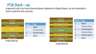
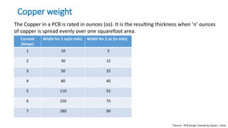
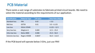
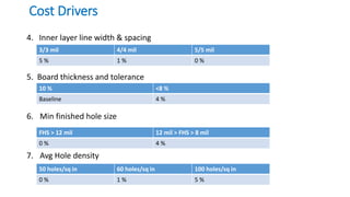
- PCB layers, stack-ups, copper weight, material selection, and surface finish which impact cost and performance.
- The PCB fabrication process involves creating the substrate, photoresist lamination, laser imaging, development, etching, stripping, inspection, hole drilling, solder mask application, and surface finishing.
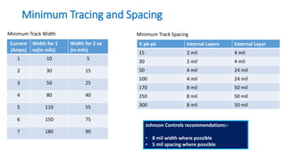
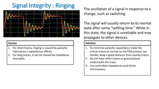
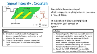
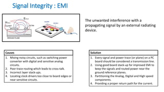
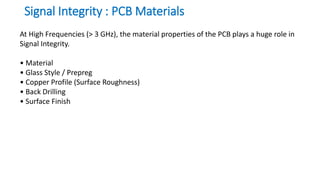
- Signal integrity is impacted by factors like ringing, crosstalk, EMI, and material properties at high frequencies. Minimizing trace length and maintaining consistent impedance can help reduce these effects.