Download to read offline
![IJRET: International Journal of Research in Engineering and Technology eISSN: 2319-1163 | pISSN: 2321-7308
__________________________________________________________________________________________________
Volume: 03 Issue: 05 | May-2014, Available @ http://www.ijret.org 441
ENHANCED LOW POWER, FAST AND AREA EFFICIENT CARRY
SELECT ADDER
Prajwal S1
1
MTech (Digital Electronics and Communication), MSRIT, Bangalore, India
Abstract
Adder being the basic hardware block of any arithmetic operation, the major constraint in the field of signal processors, data
processors to perform any operations is highly dependent on the adder performance of the circuit. The gate level implementation
of the carry select adder (CSLA) and modified carry select adder has significantly reduced the area and power consumption
which replaced the ripple carry adder (RCA) used in modified CSLA with MUX based Full Adder (MUX-FA) block has further
reduced the power consumption by efficiently utilizing the area with faster performance.
Keywords—Application-specific integrated circuit (ASIC), area efficient, MUX-FA, CSLA, low power.
-------------------------------------------------------------------***-----------------------------------------------------------------------
1. INTRODUCTION
Switching speed with low power consumption is the major
area needed to be concentrated in modern trends of signal
processing, data processing and VLSI applications. To
perform any kind of signal and data processing operation,
fast arithmetic functions are to be calculated with higher
speed but non-degrading functionality. With the advancements
in the technology the factors to be taken care during the
hardware designs are frequency or speed of operation, power
consumption, area utilization, circuit complexity, portability,
robustness etc. Thus while designing a modern high
performance processing element the optimization or best
utilization of the above mention factors are to be considered.
In any modern processing element the digital adder block is a
basic block which ensures the high- speed performance to a
large extend. The drawback of a simple ripple carry adder
(RCA) is associated with its propagation of carry bit which
is highly overcome by the implementation of high-speed,
area efficient carry select adder (CSLA)[1]. The traditional
CSLA independently generates multiple carry and then with
the selected carry generates the sum which reduces the carry
propagation delay of the RCA. The CSLA has been
modified further by reducing the area and power consumption
[2] to [4]. The implementation of square- root CSLA (SQRT
CSLA) [5] & [6] is modified with the usage of binary to
excess-1 converter (BEC) instead of RCA [7] which
claims an improved performance.
In this paper the usage of an element ripple carry adder is
eliminated and instead a MUX-FA based arithmetic adder
block is used which proves to be logically stronger with a
reduced propagation delay in comparison to the other
existing logic styles for full-adders such as standard
CMOS, complementary pass transistor logic (CPL), double
pass transistor logic (DPL), swing restored CPL (SR-CPL)
[8].
2. MUX –FA BLOCK
The main idea of this paper is to replace RCA from modified
CSLA by a MUX-FA unit for improved performance. The
MUX being a faster hardware than direct adder block
mainly improvises the performance in terms of delay, area
and power consumption. The truth table of full adder is
studied and shown in table.1 with respect to carry input (Cin).
Table.1: Truth table of FA with respect to Cin.
The MUX-FA (1-bit) implementation is shown in figure.1
The BEC based carry select addition happens by following
the algorithm below:
Cin A B Sum Carry
0 0 0 0 X
O
R
0 A
N
D
0 0 1 1 0
0 1 0 1 0
0 1 1 0 1
1 0 0 1 X
N
O
R
0 O
R1 0 1 0 1
1 1 0 0 1
1 1 1 1 1](https://image.slidesharecdn.com/enhancedlowpowerfastandareaefficientcarryselectadder-140819061634-phpapp02/85/Enhanced-low-power-fast-and-area-efficient-carry-select-adder-1-320.jpg)
![IJRET: International Journal of Research in Engineering and Technology eISSN: 2319-1163 | pISSN: 2321-7308
__________________________________________________________________________________________________
Volume: 03 Issue: 05 | May-2014, Available @ http://www.ijret.org 441
ENHANCED LOW POWER, FAST AND AREA EFFICIENT CARRY
SELECT ADDER
Prajwal S1
1
MTech (Digital Electronics and Communication), MSRIT, Bangalore, India
Abstract
Adder being the basic hardware block of any arithmetic operation, the major constraint in the field of signal processors, data
processors to perform any operations is highly dependent on the adder performance of the circuit. The gate level implementation
of the carry select adder (CSLA) and modified carry select adder has significantly reduced the area and power consumption
which replaced the ripple carry adder (RCA) used in modified CSLA with MUX based Full Adder (MUX-FA) block has further
reduced the power consumption by efficiently utilizing the area with faster performance.
Keywords—Application-specific integrated circuit (ASIC), area efficient, MUX-FA, CSLA, low power.
-------------------------------------------------------------------***-----------------------------------------------------------------------
1. INTRODUCTION
Switching speed with low power consumption is the major
area needed to be concentrated in modern trends of signal
processing, data processing and VLSI applications. To
perform any kind of signal and data processing operation,
fast arithmetic functions are to be calculated with higher
speed but non-degrading functionality. With the advancements
in the technology the factors to be taken care during the
hardware designs are frequency or speed of operation, power
consumption, area utilization, circuit complexity, portability,
robustness etc. Thus while designing a modern high
performance processing element the optimization or best
utilization of the above mention factors are to be considered.
In any modern processing element the digital adder block is a
basic block which ensures the high- speed performance to a
large extend. The drawback of a simple ripple carry adder
(RCA) is associated with its propagation of carry bit which
is highly overcome by the implementation of high-speed,
area efficient carry select adder (CSLA)[1]. The traditional
CSLA independently generates multiple carry and then with
the selected carry generates the sum which reduces the carry
propagation delay of the RCA. The CSLA has been
modified further by reducing the area and power consumption
[2] to [4]. The implementation of square- root CSLA (SQRT
CSLA) [5] & [6] is modified with the usage of binary to
excess-1 converter (BEC) instead of RCA [7] which
claims an improved performance.
In this paper the usage of an element ripple carry adder is
eliminated and instead a MUX-FA based arithmetic adder
block is used which proves to be logically stronger with a
reduced propagation delay in comparison to the other
existing logic styles for full-adders such as standard
CMOS, complementary pass transistor logic (CPL), double
pass transistor logic (DPL), swing restored CPL (SR-CPL)
[8].
2. MUX –FA BLOCK
The main idea of this paper is to replace RCA from modified
CSLA by a MUX-FA unit for improved performance. The
MUX being a faster hardware than direct adder block
mainly improvises the performance in terms of delay, area
and power consumption. The truth table of full adder is
studied and shown in table.1 with respect to carry input (Cin).
Table.1: Truth table of FA with respect to Cin.
The MUX-FA (1-bit) implementation is shown in figure.1
The BEC based carry select addition happens by following
the algorithm below:
Cin A B Sum Carry
0 0 0 0 X
O
R
0 A
N
D
0 0 1 1 0
0 1 0 1 0
0 1 1 0 1
1 0 0 1 X
N
O
R
0 O
R1 0 1 0 1
1 1 0 0 1
1 1 1 1 1](https://image.slidesharecdn.com/enhancedlowpowerfastandareaefficientcarryselectadder-140819061634-phpapp02/75/Enhanced-low-power-fast-and-area-efficient-carry-select-adder-1-2048.jpg)
![IJRET: International Journal of Research in Engineering and Technology eISSN: 2319-1163 | pISSN: 2321-7308
__________________________________________________________________________________________________
Volume: 03 Issue: 05 | May-2014, Available @ http://www.ijret.org 443
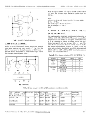
5. PROPOSED DESIGN
The proposed design replaces the regular RCA for calculating
the higher bit summation by MUX-FA. This MUX–FA
being faster and low power consumable block improves the
overall performance of the circuit. In the proposed design, as
shown in figure.3, the first bit is calculated using a direct
one bit MUX-FA block to calculate SUM0. The next higher
order bits are calculated in two parts i.e. for Cin=‘0‘ where it‘s
a simple carry addition using MUX-FA blocks & the other
one for Cin=‘1‘ using BEC. Both the output sets from
MUX-FA blocks and BEC is given as the input to 8:4MUX
and the final output of sum and carry are taken from the
MUX output. Figure .3 depicts the 4-bit implementation of
MUX-FA & BEC based CSLA which can be extended for
higher bits.
Fig 3: 4-bit RCA/MUX-FA & BEC based CSLA
6. SIMULATION
The design proposed in this paper has been developed using
Verilog - HDL and synthesized using Cadence RTL.
Simulation is done using Cadence Simvision. Table.3 shows
the simulation results for the different modules used in this
paper regarding delay, power consumption, area, Power -
Delay Product (PDP) & Area-Delay Product (ADP). The
total power is the sum of leakage power & switching power
where as the area indicates the total cell area of the design.
CONCLUSIONS
With reference from table.4 the usage of MUX-FA & BEC
based CSLA has 48.3% of improvement in PDP and 33.04 %
of improvement in ADP in comparison to modified CSLA (4-
bit, can be extended for higher bit size) and delay reduces by
34.63%. Thus with maintaining optimization & proper
functionality MUX-FA & BEC based CSLA claims to be
highly efficient. The similar work can be extended for higher
order bits i.e. for higher word size and implemented to use in
modern processors.
REFERENCES
[1]. O.J. Bedrij, ―Carry-select adder,‖IRE Tran‘s. Electron.
Comput., pp.340–344, 1962.
[2]. B. Ramkumar, H. M. Kittur, and P. M. Kannan, ―ASIC
implementation of modified faster carry save adder,‖Eur. J.
Sci. Res., vol. 42, no. 1, pp. 53–58, 2010.
[3]. T. Y. Ceiang and M. J. Hsiao, ―Carry-select adder using
single ripple carry adder,‖Electron. Lett., vol. 34, no. 22,
pp. 2101–2103, Oct. 1998..
[4]. J. M. Rabaey, Digtal Integrated Circuits—A Design
Perspective. Upper Saddle River, NJ: Prentice-Hall, 2001.
[5]. Y. He, C. H. Chang, and J. Gu, ―An area efficient 64-
bit square root carry-select adder for low power
applications,‖ inProc. IEEE Int. Symp. Circuits Syst., 2005,
vol. 4, pp. 4082–4085.
[6]. B.Ramkumar and Harish M Kittur, ―Low power area
efficient Carry select adder‖, IEEE transaction on VLSI
Systems, Vol: 20, No.2, February 2012, pp. 371–375.
4-bit RCA with BEC 1.588 123 71.783 3077.694 3149.477 5001.369 195.324
4-bit MUX- FA with BEC
(proposed model)
1.138 126 61.417 2428.017 2489.434 2584.032 130.788](https://image.slidesharecdn.com/enhancedlowpowerfastandareaefficientcarryselectadder-140819061634-phpapp02/85/Enhanced-low-power-fast-and-area-efficient-carry-select-adder-3-320.jpg)

The document presents an enhanced low power, fast, and area-efficient carry select adder (CSLA) design that incorporates a modified multiplexer-based full adder (mux-FA) and a binary to excess-1 converter (BEC) to improve performance metrics like power consumption and delay. The proposed design shows significant improvements in power-delay product (PDP) and area-delay product (ADP) compared to traditional carry adder structures, demonstrating optimized functionality suitable for integration in modern digital processing applications. Simulation results validate the efficiency of the proposed concept, indicating its potential for higher-order bit applications.