International Journal of Engineering Research and Applications (IJERA) is an open access online peer reviewed international journal that publishes research and review articles in the fields of Computer Science, Neural Networks, Electrical Engineering, Software Engineering, Information Technology, Mechanical Engineering, Chemical Engineering, Plastic Engineering, Food Technology, Textile Engineering, Nano Technology & science, Power Electronics, Electronics & Communication Engineering, Computational mathematics, Image processing, Civil Engineering, Structural Engineering, Environmental Engineering, VLSI Testing & Low Power VLSI Design etc.
VLSI Projects for M. Tech, VLSI Projects in Vijayanagar, VLSI Projects in Bangalore, M. Tech Projects in Vijayanagar, M. Tech Projects in Bangalore, VLSI IEEE projects in Bangalore, IEEE 2015 VLSI Projects, FPGA and Xilinx Projects, FPGA and Xilinx Projects in Bangalore, FPGA and Xilinx Projects in Vijayangar
International Journal of Engineering Research and Applications (IJERA) is an open access online peer reviewed international journal that publishes research and review articles in the fields of Computer Science, Neural Networks, Electrical Engineering, Software Engineering, Information Technology, Mechanical Engineering, Chemical Engineering, Plastic Engineering, Food Technology, Textile Engineering, Nano Technology & science, Power Electronics, Electronics & Communication Engineering, Computational mathematics, Image processing, Civil Engineering, Structural Engineering, Environmental Engineering, VLSI Testing & Low Power VLSI Design etc.
In this paper, we propose a new technique for implementing a low power high speed multiplier based on Sleepy Stack Technique and consisting of
minimum number of transistors. Multiplier circuits are used comprehensively in Application Specific Integrated Circuits (ASICs). An 4 bit x 4 bit
multiplier has also been implemented using the design of only using basic combinational circuits and its performance has been analyzed and
compared with similar multipliers designed with peer combinational design available in literature. The explored method of implementation achieves
a high speed low power design for the multiplier. Simulated results indicate the superior performance of the proposed technique over conventional
CMOS multiplier. Detailed comparison of simulated results for the conventional and present method of implementation is presented.
International Journal of Engineering Research and Applications (IJERA) is an open access online peer reviewed international journal that publishes research and review articles in the fields of Computer Science, Neural Networks, Electrical Engineering, Software Engineering, Information Technology, Mechanical Engineering, Chemical Engineering, Plastic Engineering, Food Technology, Textile Engineering, Nano Technology & science, Power Electronics, Electronics & Communication Engineering, Computational mathematics, Image processing, Civil Engineering, Structural Engineering, Environmental Engineering, VLSI Testing & Low Power VLSI Design etc.
Implementation of Area & Power Optimized VLSI Circuits Using Logic TechniquesIOSRJVSP
To achieve the reduction of power consumption, optimizations are required at various levels of the design steps such as algorithm, architecture, logic and circuit & process techniques. This paper considers the two logic level approaches for low power digital design. Optimization techniques are carried to reduce switching activity power of individual logic-gates. we can reduce the power by using either circuit level optimization or logical level optimization. In this paper, the circuit level optimization process is followed to reduce the area and power. In the first approach, Modified gate diffusion input (GDI) logic is used in the proposed parallel asynchronous self time adder (PASTA) technique. Similarly, the structure of XOR gate and half adder is reduced to achieve the low area and low power. In second approach, Multi value logic based digital circuit is designed by increasing the representation domain from the two level (N=2) switching algebra to N > 2 levels. The main advantage of this approach is to compensate the inefficiency of existing integrated circuits that are used to implement the universal set of MVL gates. From the results, the proposed GDL logic based Adder offers less number of transistors (area) and low power consumption than the existing technique. And proposed MVL technique allows designing MVL digital circuit that is set to obtain the values from the binary circuits. Also this technique offers low power and small wiring delay, when compared to binary and three value logic. The simulation process is carried out by tanner toolv14.11 to check the functionality of the PASTA & MVL circuits.
Implementation of Low Power and Area Efficient Carry Select Adderinventionjournals
International Journal of Engineering and Science Invention (IJESI) is an international journal intended for professionals and researchers in all fields of computer science and electronics. IJESI publishes research articles and reviews within the whole field Engineering Science and Technology, new teaching methods, assessment, validation and the impact of new technologies and it will continue to provide information on the latest trends and developments in this ever-expanding subject. The publications of papers are selected through double peer reviewed to ensure originality, relevance, and readability. The articles published in our journal can be accessed online.
Design and Verification of Area Efficient Carry Select Adderijsrd.com
Carry Select Adder (CSLA) is one of the fastest adders used in many data-processing processors to perform fast arithmetic functions. From the structure of the CSLA, it is clear that there is scope for reducing the area and power consumption in the CSLA. This work uses a simple and efficient gate-level modification to significantly reduce the area and power of the CSLA. Based on this modification 16, 32 square - root CSLA (SQRT CSLA) architecture have been developed and compared with the regular SQRT CSLA architecture. The proposed design has reduced area and power as compared with the regular SQRT CSLA with only a slight increase in the delay. This work evaluates the performance of the proposed designs in terms of delay, area.
A comparative study of full adder using static cmos logic styleeSAT Publishing House
IJRET : International Journal of Research in Engineering and Technology is an international peer reviewed, online journal published by eSAT Publishing House for the enhancement of research in various disciplines of Engineering and Technology. The aim and scope of the journal is to provide an academic medium and an important reference for the advancement and dissemination of research results that support high-level learning, teaching and research in the fields of Engineering and Technology. We bring together Scientists, Academician, Field Engineers, Scholars and Students of related fields of Engineering and Technology.
Layout Design Analysis of CMOS Comparator using 180nm TechnologyIJEEE
Comparator is a very useful and basic arithmetic component of digital system. In the world of technology the demand of portable devices are increasing day by day. This paper presents CMOS design of 1-bit comparator on 180nm technology. The layout of 1-bit comparator has been developed using Automatic and semi-custom techniques. Both the layouts are compared and analyzed in terms of their Power and Area consumption. Automatic layout is generated from its equivalent schematic whereas semi-custom layout is developed manually. The result shows that semi-custom consumes less power as compared to Automatic.
International Journal of Engineering Research and Applications (IJERA) is an open access online peer reviewed international journal that publishes research and review articles in the fields of Computer Science, Neural Networks, Electrical Engineering, Software Engineering, Information Technology, Mechanical Engineering, Chemical Engineering, Plastic Engineering, Food Technology, Textile Engineering, Nano Technology & science, Power Electronics, Electronics & Communication Engineering, Computational mathematics, Image processing, Civil Engineering, Structural Engineering, Environmental Engineering, VLSI Testing & Low Power VLSI Design etc.
An efficient model for design of 64-bit High Speed Parallel Prefix VLSI adderIJMER
International Journal of Modern Engineering Research (IJMER) is Peer reviewed, online Journal. It serves as an international archival forum of scholarly research related to engineering and science education.
International Journal of Computational Engineering Research(IJCER) is an intentional online Journal in English monthly publishing journal. This Journal publish original research work that contributes significantly to further the scientific knowledge in engineering and Technology.
Design of 8-Bit Comparator Using 45nm CMOS TechnologyIJMER
In this paper design of 8- bit binary comparator using 45nm CMOS technology is discussed.
This design needs less area and less number of transistors, also discussed about power and execution time. The
circuit has three output X, Y and Z. X is active high, when A>B, Y is active high when A=B and Z is active high
when both X and Y are active low. Design 1- bit comparator with the help of precharge gate.The design of 1-bit
comparator has been extended to implement an 8-bit comparator by connecting in series with pass
transistor between them. The design has been implemented in Microwind3.1, is tested successfully and
has been validated using Pspice for different measurable parameter.
Highly -increasing requirement for mobile and several electronic devices want the use of VLSI circuits which are highly power efficient. The most primitive arithmetic operation in processors is addition and the adder is the most highly used arithmetic component of the processor. Carry Select Adder (CSA) is one of the fastest adders and the structure of the CSA shows that there is a possibility for increasing its efficiency by reducing the power dissipation and area in the CSA. This research paper presents power and delay analysis of various adders and proposed a 32-bit CSA that is implemented using variable size of the combination of adders, thus the proposed Carry select Adder (CSA) which has minimum Delay, and less power consumption hence improving the efficiency and speed of the Carry Select Adder.
Design and Implementation of Low-Power and Area-Efficient 64 bit CSLA using VHDLIJSRD
All processor consisting ALU and adder plays important role for design of ALU. Design of low area and power efficient adder helps to reduce power consumption and area of any processor. Now a day’s major area of research in VLSI system is design of area, high speed and low power data path logic systems. In digital adders, the speed of addition is restricted by the time necessary to send a carry signal through the adder. The area and power consumption is reduced by modifying regular CSLA architecture. The proposed architecture is developed with the help of a simple ripple carry adder (RCA) and gate-level architecture. It consists of single RCA which improves the performance of the proposed designs then the regular designs in terms of power consumption and area.
International Journal of Engineering Research and Applications (IJERA) is an open access online peer reviewed international journal that publishes research and review articles in the fields of Computer Science, Neural Networks, Electrical Engineering, Software Engineering, Information Technology, Mechanical Engineering, Chemical Engineering, Plastic Engineering, Food Technology, Textile Engineering, Nano Technology & science, Power Electronics, Electronics & Communication Engineering, Computational mathematics, Image processing, Civil Engineering, Structural Engineering, Environmental Engineering, VLSI Testing & Low Power VLSI Design etc.
IJERA (International journal of Engineering Research and Applications) is International online, ... peer reviewed journal. For more detail or submit your article, please visit www.ijera.com
International Journal of Engineering Research and Applications (IJERA) is an open access online peer reviewed international journal that publishes research and review articles in the fields of Computer Science, Neural Networks, Electrical Engineering, Software Engineering, Information Technology, Mechanical Engineering, Chemical Engineering, Plastic Engineering, Food Technology, Textile Engineering, Nano Technology & science, Power Electronics, Electronics & Communication Engineering, Computational mathematics, Image processing, Civil Engineering, Structural Engineering, Environmental Engineering, VLSI Testing & Low Power VLSI Design etc.
Estratégias para Buscadores - Pensando SocialFabio Ricotta
Palestra oferecida pelo Fábio Ricotta, Co-Fundador da MestreSEO, para o Digitalks Day em Belo Horizonte, focando estratégias de conteúdo que possuem impacto para usuários, dando a possibilidade de influenciar os resultados orgânicos dos .
IJRET : International Journal of Research in Engineering and Technology is an international peer reviewed, online journal published by eSAT Publishing House for the enhancement of research in various disciplines of Engineering and Technology. The aim and scope of the journal is to provide an academic medium and an important reference for the advancement and dissemination of research results that support high-level learning, teaching and research in the fields of Engineering and Technology. We bring together Scientists, Academician, Field Engineers, Scholars and Students of related fields of Engineering and Technology
International Journal of Engineering Research and Applications (IJERA) is an open access online peer reviewed international journal that publishes research and review articles in the fields of Computer Science, Neural Networks, Electrical Engineering, Software Engineering, Information Technology, Mechanical Engineering, Chemical Engineering, Plastic Engineering, Food Technology, Textile Engineering, Nano Technology & science, Power Electronics, Electronics & Communication Engineering, Computational mathematics, Image processing, Civil Engineering, Structural Engineering, Environmental Engineering, VLSI Testing & Low Power VLSI Design etc.
FPGA Implementation of High Speed Architecture of CSLA using D-LatchesEditor IJMTER
Carry Select Adder (CSLA) is one of the fastest adders used in many data-processing
processors to perform fast arithmetic functions. The CSLA is used in many systems to overcome the
problem of carry propagation delay by independently generating multiple carries and then select a
carry to generate the sum. But the CSLA is not area efficient because it uses multiple pairs of Ripple
Carry Adders (RCA). Due to the rapidly growing mobile industry not only the faster arithmetic unit
but also less area and low power arithmetic units are needed. The modified CSLA architecture has
developed using Binary to Excess-1 converter (BEC). This paper proposes an efficient method which
replaces the BEC using D latch. Designs were developed using structural VHDL and synthesized in
Xilinx 13.2 with reference to FPGA device XC3S500E.
Area Delay Power Efficient and Implementation of Modified Square-Root Carry S...IJTET Journal
Abstract: In VLSI Technology, Carry Propagation Delay is the most important concern for the Adders. Adder is the most unavoidable component for the arithmetic performances. This paper is Modified Square Root-Carry Select Adder (SQRT-CSLA) design reduces the delay with 16 bit adder. Carry select adder have two units for Carry Generation (CG) and Carry Selection (CS). The modified SQRT-CSLA design can gives parallel path for carry propagation. So the overall adder delay has reduced. Modified design is obtained using Ripple Carry Adder (RCA) with Boolean Excess-1 Converter (BEC). BEC produces an output i.e., is an excess one result for given input bits. Then input bits and BEC output is given to multiplexer for carry selection. Use of BEC instead of dual RCA gives efficient carry propagation delay and it consumes the lower power and overall gates using in design is reduced with compared to carry select adder with dual RCA. The final sum is calculated using final sum generation.
128-Bit Area Efficient Reconfigurable Carry Select Adder ijcisjournal
Adders are one of the most critical arithmetic circuits in a system and their throughput affects the overall
performance of the system. Carry Select Adder (CSLA) is one of the fastest adders used in many dataprocessing
processors to perform fast arithmetic functions. From the structure of the CSLA, it is clear that
there is scope for reducing the area and power consumption in the CSLA. In this paper, we proposed an
area-efficient carry select adder by sharing the common Boolean logic term. After logic optimization and
sharing partial circuit, we only need one XOR gate and one inverter gate for sum generation. Through the
multiplexer, we can select the final-sum only and for carry selection we need only one AND gate and one
OR gate. Based on this modification 16-, 32-, 64-, and 128-bit CSLA architecture have been developed and
compared with the conventional CSLA architecture. The proposed design greatly reduces the area
compared to other CSLAs. From this improvement, the gate count of a 128-bit carry select adder can be
reduced from 3320 to 1664. The proposed structure is implemented in Artix-7 FPGA. Compared with the
proposed design, the conventional CSLA has 65.80% less area.
IJERA (International journal of Engineering Research and Applications) is International online, ... peer reviewed journal. For more detail or submit your article, please visit www.ijera.com
Duet advancement of new technology in the field of VLSI and Embedded system, there is an increasing demand of high speed and low power consumption processor. Speed of processor greatly depends on its multiplier as well as adder performance. Due to which high speed adder architecture become important. Sever a ladder architecture designs have been developed to increase the efficiency of the adder. In this paper, we introduce an architecture that performs high speed modified carry select adder using boot hen coder (BEC) Technique. Booth encoder, Mathematics is an ancient Indian system of Mathematics. Here we are introduced two carry select based design. These designs are implementation Xilinx Vertex device family.
Area, Delay and Power Comparison of Adder TopologiesVLSICS Design
Adders form an almost obligatory component of every contemporary integrated circuit. The prerequisite of the adder is that it is primarily fast and secondarily efficient in terms of power consumption and chip area. This paper presents the pertinent choice for selecting the adder topology with the tradeoff between delay, power consumption and area. The adder topology used in this work are ripple carry adder, carry lookahead adder, carry skip adder, carry select adder, carry increment adder, carry save adder and carry bypass adder. The module functionality and performance issues like area, power dissipation and propagation delay are analyzed at 0.12µm 6metal layer CMOS technology using microwind tool.
High Speed and Area Efficient Booth Multiplier Using SQRT CSLA with Zero Find...IJERA Editor
Addition is one of the common and widely used fundamental arithmetic operation in many VLSI systems. The critical elements in general purpose and digital-signal processing processors are High performance VLSI integer adders as they are employed in the design of Arithmetic-Logic Units, in floating-point arithmetic data paths and in address generation units. The performance parameters for any adder are area, speed and delay. By using Square Root Carry Select Adder (SQRT CSLA), speed can be achieved. In designing new architecture, the Tradeoff between those parameters plays the major role. We can reduce area by using Zero Finding Logic (ZFC) technique, from the structure of SQRT CSLA. By using the Modified architecture we can reduce area. We can implement Booth multiplier by using the CSLA and SQRT CSLA with Zero finding logic. Implementation of Booth multiplier by using CSLA and SQRT CSLA with Zero finding logic is proposed for better speed applications and efficient area applications.
PERFORMANCE EVALUATION OF LOW POWER CARRY SAVE ADDER FOR VLSI APPLICATIONSVLSICS Design
This report examines the subject of sub threshold leakage on carry save adder. When the gate to source voltage reduces to the threshold voltage at that place is yet some amount of current flow in the circuit and that is undesired. As the process technology advancing much rapidly the threshold voltage of MOS devices reduces very drastically, and it must be applied in lower power devices since it contributes to low amount of leakage current which confine increases the power consumption of the devices. Adders are the basic building blocks for any digital circuit design and used in almost all arithmetic’s. The CSA proves efficient adders due to its quick and precise computations. Hence this paper performs sub threshold analysis on CSA and the scrutinize results that the total average power is around 4.93µW, the propagation delay for complete operation is 16.3ns and since this design uses GDI cell so there is a reduction in area with 37%.
PERFORMANCE EVALUATION OF LOW POWER CARRY SAVE ADDER FOR VLSI APPLICATIONSVLSICS Design
This report examines the subject of sub threshold leakage on carry save adder. When the gate to source voltage reduces to the threshold voltage at that place is yet some amount of current flow in the circuit and that is undesired. As the process technology advancing much rapidly the threshold voltage of MOS devices reduces very drastically, and it must be applied in lower power devices since it contributes to low amount
of leakage current which confine increases the power consumption of the devices. Adders are the basic
building blocks for any digital circuit design and used in almost all arithmetic’s. The CSA proves efficient adders due to its quick and precise computations. Hence this paper performs sub threshold analysis on CSA and the scrutinize results that the total average power is around 4.93µW, the propagation delay for complete operation is 16.3ns and since this design uses GDI cell so there is a reduction in area with 37%.
PERFORMANCE EVALUATION OF LOW POWER CARRY SAVE ADDER FOR VLSI APPLICATIONSVLSICS Design
This report examines the subject of sub threshold leakage on carry save adder. When the gate to source voltage reduces to the threshold voltage at that place is yet some amount of current flow in the circuit and that is undesired. As the process technology advancing much rapidly the threshold voltage of MOS devices reduces very drastically, and it must be applied in lower power devices since it contributes to low amount of leakage current which confine increases the power consumption of the devices. Adders are the basic building blocks for any digital circuit design and used in almost all arithmetic’s. The CSA proves efficient adders due to its quick and precise computations. Hence this paper performs sub threshold analysis on CSA and the scrutinize results that the total average power is around 4.93µW, the propagation delay for complete operation is 16.3ns and since this design uses GDI cell so there is a reduction in area with 37%
Power Efficient and High Speed Carry Skip Adder using Binary to Excess One Co...rahulmonikasharma
The design of high-speed and low-power VLSI architectures need efficient arithmetic processing units, which are optimized for the performance parameters, namely, speed and power consumption. Adders are the key components in general purpose microprocessors and digital signal processors. As a result, it is very pertinent that its performance augers well for their speed performance. Additionally, the area is an essential factor which is to be taken into account in the design of fast adders. Towards this end, high-speed, low power and area efficient addition and multiplication have always been a fundamental requirement of high-performance processors and systems. The major speed limitation of adders arises from the huge carry propagation delay encountered in the conventional adder circuits, such as ripple carry adder and carry save adder. Observing that a carry may skip any addition stages on certain addend and augend bit values, researchers developed the carry-skip technique to speed up addition in the carry-ripple adder. Using a multilevel structure, carry-skip logic determines whether a carry entering one block may skip the next group of blocks. Because multilevel skip logic introduces longer delays, Therefore, in this paper we examine The basic idea of this work is to use Binary to Excess- 1 converter (BEC) instead of RCA with Cin=1 in conventional CSkA in order to reduce the area and power. BEC uses less number of logic gates than N-bit full adder.
DESIGN AND IMPLEMENTATION OF AN IMPROVED CARRY INCREMENT ADDERVLSICS Design
A complex digital circuit comprises of adder as a basic unit. The performance of the circuit depends on the
design of this basic adder unit. The speed of operation of a circuit is one of the important performance
criteria of many digital circuits which ultimately depends on the delay of the basic adder unit. Many
research works have been devoted in improving the delay of the adder circuit. In this paper we have
proposed an improved carry increment adder (CIA) that improves the delay performance of the circuit. The
improvement is achieved by incorporating carry look adder (CLA) in the design of CIA contrary to the
previous design of CIA that employs ripple carry adder (RCA). A simulation study is carried out for
comparative analysis. The coding is done in Verilog hardware description language (HDL) and the
simulation is carried out in Xilinx ISE 13.1 environment.
International Journal of Engineering Research and Development (IJERD)IJERD Editor
journal publishing, how to publish research paper, Call For research paper, international journal, publishing a paper, IJERD, journal of science and technology, how to get a research paper published, publishing a paper, publishing of journal, publishing of research paper, reserach and review articles, IJERD Journal, How to publish your research paper, publish research paper, open access engineering journal, Engineering journal, Mathemetics journal, Physics journal, Chemistry journal, Computer Engineering, Computer Science journal, how to submit your paper, peer reviw journal, indexed journal, reserach and review articles, engineering journal, www.ijerd.com, research journals,
yahoo journals, bing journals, International Journal of Engineering Research and Development, google journals, hard copy of journal
IOSR Journal of Electronics and Communication Engineering(IOSR-JECE) is an open access international journal that provides rapid publication (within a month) of articles in all areas of electronics and communication engineering and its applications. The journal welcomes publications of high quality papers on theoretical developments and practical applications in electronics and communication engineering. Original research papers, state-of-the-art reviews, and high quality technical notes are invited for publications.
DevOps and Testing slides at DASA ConnectKari Kakkonen
My and Rik Marselis slides at 30.5.2024 DASA Connect conference. We discuss about what is testing, then what is agile testing and finally what is Testing in DevOps. Finally we had lovely workshop with the participants trying to find out different ways to think about quality and testing in different parts of the DevOps infinity loop.
The Art of the Pitch: WordPress Relationships and SalesLaura Byrne
Clients don’t know what they don’t know. What web solutions are right for them? How does WordPress come into the picture? How do you make sure you understand scope and timeline? What do you do if sometime changes?
All these questions and more will be explored as we talk about matching clients’ needs with what your agency offers without pulling teeth or pulling your hair out. Practical tips, and strategies for successful relationship building that leads to closing the deal.
Key Trends Shaping the Future of Infrastructure.pdfCheryl Hung
Keynote at DIGIT West Expo, Glasgow on 29 May 2024.
Cheryl Hung, ochery.com
Sr Director, Infrastructure Ecosystem, Arm.
The key trends across hardware, cloud and open-source; exploring how these areas are likely to mature and develop over the short and long-term, and then considering how organisations can position themselves to adapt and thrive.
Slack (or Teams) Automation for Bonterra Impact Management (fka Social Soluti...Jeffrey Haguewood
Sidekick Solutions uses Bonterra Impact Management (fka Social Solutions Apricot) and automation solutions to integrate data for business workflows.
We believe integration and automation are essential to user experience and the promise of efficient work through technology. Automation is the critical ingredient to realizing that full vision. We develop integration products and services for Bonterra Case Management software to support the deployment of automations for a variety of use cases.
This video focuses on the notifications, alerts, and approval requests using Slack for Bonterra Impact Management. The solutions covered in this webinar can also be deployed for Microsoft Teams.
Interested in deploying notification automations for Bonterra Impact Management? Contact us at sales@sidekicksolutionsllc.com to discuss next steps.
GDG Cloud Southlake #33: Boule & Rebala: Effective AppSec in SDLC using Deplo...James Anderson
Effective Application Security in Software Delivery lifecycle using Deployment Firewall and DBOM
The modern software delivery process (or the CI/CD process) includes many tools, distributed teams, open-source code, and cloud platforms. Constant focus on speed to release software to market, along with the traditional slow and manual security checks has caused gaps in continuous security as an important piece in the software supply chain. Today organizations feel more susceptible to external and internal cyber threats due to the vast attack surface in their applications supply chain and the lack of end-to-end governance and risk management.
The software team must secure its software delivery process to avoid vulnerability and security breaches. This needs to be achieved with existing tool chains and without extensive rework of the delivery processes. This talk will present strategies and techniques for providing visibility into the true risk of the existing vulnerabilities, preventing the introduction of security issues in the software, resolving vulnerabilities in production environments quickly, and capturing the deployment bill of materials (DBOM).
Speakers:
Bob Boule
Robert Boule is a technology enthusiast with PASSION for technology and making things work along with a knack for helping others understand how things work. He comes with around 20 years of solution engineering experience in application security, software continuous delivery, and SaaS platforms. He is known for his dynamic presentations in CI/CD and application security integrated in software delivery lifecycle.
Gopinath Rebala
Gopinath Rebala is the CTO of OpsMx, where he has overall responsibility for the machine learning and data processing architectures for Secure Software Delivery. Gopi also has a strong connection with our customers, leading design and architecture for strategic implementations. Gopi is a frequent speaker and well-known leader in continuous delivery and integrating security into software delivery.
Elevating Tactical DDD Patterns Through Object CalisthenicsDorra BARTAGUIZ
After immersing yourself in the blue book and its red counterpart, attending DDD-focused conferences, and applying tactical patterns, you're left with a crucial question: How do I ensure my design is effective? Tactical patterns within Domain-Driven Design (DDD) serve as guiding principles for creating clear and manageable domain models. However, achieving success with these patterns requires additional guidance. Interestingly, we've observed that a set of constraints initially designed for training purposes remarkably aligns with effective pattern implementation, offering a more ‘mechanical’ approach. Let's explore together how Object Calisthenics can elevate the design of your tactical DDD patterns, offering concrete help for those venturing into DDD for the first time!
Essentials of Automations: Optimizing FME Workflows with ParametersSafe Software
Are you looking to streamline your workflows and boost your projects’ efficiency? Do you find yourself searching for ways to add flexibility and control over your FME workflows? If so, you’re in the right place.
Join us for an insightful dive into the world of FME parameters, a critical element in optimizing workflow efficiency. This webinar marks the beginning of our three-part “Essentials of Automation” series. This first webinar is designed to equip you with the knowledge and skills to utilize parameters effectively: enhancing the flexibility, maintainability, and user control of your FME projects.
Here’s what you’ll gain:
- Essentials of FME Parameters: Understand the pivotal role of parameters, including Reader/Writer, Transformer, User, and FME Flow categories. Discover how they are the key to unlocking automation and optimization within your workflows.
- Practical Applications in FME Form: Delve into key user parameter types including choice, connections, and file URLs. Allow users to control how a workflow runs, making your workflows more reusable. Learn to import values and deliver the best user experience for your workflows while enhancing accuracy.
- Optimization Strategies in FME Flow: Explore the creation and strategic deployment of parameters in FME Flow, including the use of deployment and geometry parameters, to maximize workflow efficiency.
- Pro Tips for Success: Gain insights on parameterizing connections and leveraging new features like Conditional Visibility for clarity and simplicity.
We’ll wrap up with a glimpse into future webinars, followed by a Q&A session to address your specific questions surrounding this topic.
Don’t miss this opportunity to elevate your FME expertise and drive your projects to new heights of efficiency.
UiPath Test Automation using UiPath Test Suite series, part 3DianaGray10
Welcome to UiPath Test Automation using UiPath Test Suite series part 3. In this session, we will cover desktop automation along with UI automation.
Topics covered:
UI automation Introduction,
UI automation Sample
Desktop automation flow
Pradeep Chinnala, Senior Consultant Automation Developer @WonderBotz and UiPath MVP
Deepak Rai, Automation Practice Lead, Boundaryless Group and UiPath MVP
JMeter webinar - integration with InfluxDB and GrafanaRTTS
Watch this recorded webinar about real-time monitoring of application performance. See how to integrate Apache JMeter, the open-source leader in performance testing, with InfluxDB, the open-source time-series database, and Grafana, the open-source analytics and visualization application.
In this webinar, we will review the benefits of leveraging InfluxDB and Grafana when executing load tests and demonstrate how these tools are used to visualize performance metrics.
Length: 30 minutes
Session Overview
-------------------------------------------
During this webinar, we will cover the following topics while demonstrating the integrations of JMeter, InfluxDB and Grafana:
- What out-of-the-box solutions are available for real-time monitoring JMeter tests?
- What are the benefits of integrating InfluxDB and Grafana into the load testing stack?
- Which features are provided by Grafana?
- Demonstration of InfluxDB and Grafana using a practice web application
To view the webinar recording, go to:
https://www.rttsweb.com/jmeter-integration-webinar
Neuro-symbolic is not enough, we need neuro-*semantic*Frank van Harmelen
Neuro-symbolic (NeSy) AI is on the rise. However, simply machine learning on just any symbolic structure is not sufficient to really harvest the gains of NeSy. These will only be gained when the symbolic structures have an actual semantics. I give an operational definition of semantics as “predictable inference”.
All of this illustrated with link prediction over knowledge graphs, but the argument is general.
When stars align: studies in data quality, knowledge graphs, and machine lear...
Bu34437441
1. B.Bharathi1
C.V.Subhaskar Reddy / International Journal of Engineering Research and
Applications (IJERA) ISSN: 2248-9622 www.ijera.com
Vol. 3, Issue 4, Jul-Aug 2013, pp. 437-441
437 | P a g e
Design of an Efficient 128-Bit Carry Select Adder Using Bec and
Variable csla Techniques
B.Bharathi1
, C.V.Subhaskar Reddy2
1
DEPARTMENT OF ECE, S.R.E.C, NANDYAL
2
ASSOCIATE PROFESSOR, S.R.E.C, NANDYAL.
Abstract
Design of area- and power-efficient high-
speed data path logic systems forms the largest
areas of research in VLSI system design. In
digital adders, the speed of addition is limited by
the time required to transmit a carry through the
adder. Carry Select Adder (CSLA) is one of the
fastest adders used in many data-processing
processors to perform fast arithmetic functions.
From the structure of the CSLA, it is clear that
there is span for reducing the area and power
consumption in the CSLA. This work uses a
simple and efficient gate-level modification to
drastically reduce the area and power of the
CSLA. Based on this modification 8, 16, 32, 64
and 128-bit square-root CSLA (SQRT CSLA)
architectures have been developed and compared
with the regular SQRT CSLA architecture. The
proposed design has reduced area and power as
compared with the regular SQRT CSLA with
only a minor increase in the delay. This work
estimates the performance of the proposed
designs in terms of delay, area are implemented
in Xilinx ISE and Modelsim.
I. Introduction
Area and power reduction in data path logic
systems are the main area of research in VLSI
system design. High-speed addition and
multiplication has always been a fundamental
requirement of high-performance processors and
systems. In digital adders, the speed of addition is
limited by the time required to propagate a carry
through the adder. The sum for each bit position in
an elementary adder is generated sequentially only
after the previous bit position has been summed and
a carry propagated into the next position. The major
speed limitation in any adder is in the production of
carries and many authors have considered the
addition problem.
The CSLA is used in many computational
systems to moderate the problem of carry
propagation delay by independently generating
multiple carries and then select a carry to generate
the sum. However, the CSLA is not area efficient
because it uses multiple pairs of Ripple Carry
Adders (RCA) to generate partial sum and carry by
considering carry input and then the final sum and
carry are selected by the multiplexers (mux). To
overcome above problem, the basic idea of the
proposed work is by using n-bit binary to excess-1
code converters (BEC) to improve the speed of
addition. This logic can be implemented with any
type of adder to further improve the speed. Using
Binary to Excess-1 Converter (BEC) instead of RCA
in the regular CSLA to achieve lower area and
power consumption. The main advantage of this
BEC logic comes from the lesser number of logic
gates than the Full Adder (FA) structure.
In electronics, a carry-select adder is a particular
way to implement an adder, which is a logic element
that computes the -bit sum of two -bit
numbers. The carry-select adder is simple but rather
fast, having a gate level depth of .
The carry-select adder generally consists of
two ripple carry adders and a multiplexer. Adding
two n-bit numbers with a carry-select adder is done
with two adders (therefore two ripple carry adders)
in order to perform the calculation twice, one time
with the assumption of the carry being zero and the
other assuming one. After the two results are
calculated, the correct sum, as well as the correct
carry, is then selected with the multiplexer once the
correct carry is known. The number of bits in
each carry select block can be uniform, or variable.
In the uniform case, the optimal delay occurs for a
block size of . When variable, the block size
should have a delay, from addition inputs A and B to
the carry out, equal to that of the multiplexer chain
leading into it, so that the carry out is calculated just
in time. The delay is derived from
uniform sizing, where the ideal number of full-adder
elements per block is equal to the square root of the
number of bits being added, since that will yield an
equal number of MUX delays.
Basic building block
Figure 1: Basic carry Select adder.
2. B.Bharathi1
C.V.Subhaskar Reddy / International Journal of Engineering Research and
Applications (IJERA) ISSN: 2248-9622 www.ijera.com
Vol. 3, Issue 4, Jul-Aug 2013, pp. 437-441
438 | P a g e
Above is the basic building block of a
carry-select adder, where the block size is 4. Two 4-
bit ripple carry adders are multiplexed together,
where the resulting carry and sum bits are selected
by the carry-in. Since one ripple carry adder assumes
a carry-in of 0, and the other assumes a carry-in of 1,
selecting which adder had the correct assumption via
the actual carry-in yields the desired result.
Uniform-sized adder
A 16-bit carry-select adder with a uniform
block size of 4 can be created with three of these
blocks and a 4-bit ripple carry adder. Since carry-in
is known at the beginning of computation, a carry
select block is not needed for the first four bits. The
delay of this adder will be four full adder delays,
plus three MUX delays.
Figure 2: Regular Fixed Size CSLA
Variable-sized adder
A 16-bit carry-select adder with variable
size can be similarly created. Here we show an adder
with block sizes of 2-2-3-4-5. This break-up is ideal
when the full-adder delay is equal to the MUX
delay, which is unlikely. The total delay is two full
adder delays, and four mux delays.
Figure 3: Variable Sized CSLA.
The basic idea of this work is to use Binary
to Excess-1 Converter (BEC) instead of RCA with
Cin=1 in the regular CSLA to achieve lower area
and power consumption [2]–[4]. The main
advantage of this BEC logic comes from the lesser
number of logic gates than the n-bit Full Adder (FA)
structure. The details of the BEC logic are discussed
in Section III.
This brief is structured as follows. Section
II deals with the delay and area evaluation
methodology of the basic adder blocks. Section III
presents the detailed structure and the function of the
BEC logic. The SQRT CSLA has been chosen for
comparison with the proposed design as it has a
more balanced delay, and requires lower power and
area [5], [6]. The delay and area evaluation
methodology of the regular and modified SQRT
CSLA are presented in Sections IV and V,
respectively. The ASIC implementation details and
results are analyzed in Section VI. Finally, the work
is concluded in Section VII.
II. Basic Function And Structure Of BEC
Logic
The delay and area evaluation methodology
considers all gates to be made up of AND, OR, and
Inverter, each having delay equal to 1 unit and area
equal to 1 unit. We then add up the number of gates
in the longest path of a logic block that contributes
to the maximum delay. The area evaluation is done
by counting the total number of AOI gates required
for each logic block. Based on this approach, the
CSLA adder blocks of 2:1 mux, Half Adder (HA),
and FA are evaluated and listed in Table I.
The basic work is to use Binary to Excess-1
Converter (BEC) instead of RCA with Cin=1 in the
regular CSLA to achieve lower area and power
consumption. The main advantage of this BEC logic
comes from the lesser number of logic gates than the
n-bit Full Adder (FA) structure As stated above the
main idea of this work is to use BEC instead of the
RCA with Cin=1 in order to reduce the area and
power consumption of the regular CSLA. To replace
the n-bit RCA, an n+1-bit BEC is required. A
structure and the function table of a 4-bit BEC are
shown in Figure.2 and Table .2, respectively.
Figure 1: 4 Bit BEC.
The Boolean expressions of the 4-bit BEC
is listed as (note the functional symbols ~ NOT, &
AND, ^XOR)
X0 = ~B0
X1 = B0^B1
X2 = B2^ (B0 & B1)
X3 = B3^ (B0 & B1 & B2)
3. B.Bharathi1
C.V.Subhaskar Reddy / International Journal of Engineering Research and
Applications (IJERA) ISSN: 2248-9622 www.ijera.com
Vol. 3, Issue 4, Jul-Aug 2013, pp. 437-441
439 | P a g e
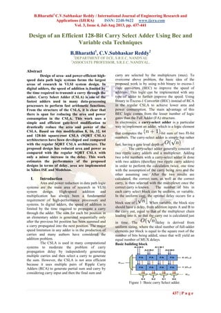
Figure 4: 4-Bit BEC with 8:4 mux.
III. Basic Structure of Regular 16-Bit
CSLA
A 16-bit carry select has two types of block
size namely uniform block size and variable block
size. A 16-bit carry select adder with a uniform
block size has the delay of four full adder delays and
three MUX delays. While a 16-bit carry select adder
with variable block size has the delay of two full
adder delays, and four mux delays. Therefore we use
16-bit carry select adder with variable block size.
Ripple-carry adders are the simplest and most
compact full adders, but their performance is limited
by a carry that must ripple from the least-significant
to the most-significant bit. A carry-select adder
achieves speeds 40% to 90% faster by performing
additions in parallel and reducing the maximum
carry path.
A carry-select adder is divided into sectors,
each of which, except for the least significant
performs two additions in parallel, one assuming a
carry-in of zero, the other a carry-in of one within
the sector, there are two 4-bit ripple- carry adders
receiving the same data inputs but different Cin. The
upper adder has a carry-in of zero, the lower adder a
carry-in of one. The actual Cin from the preceding
sector selects one of the two adders. If the carry-in is
zero, the sum and carry-out of the upper adder are
selected. If the carry-in is one, the sum and carry-out
of the lower adder are selected. Logically, the result
is not different if a single ripple-carry adder were
used.
First the coding for full adder and different
multiplexers of 6:3, 8:4, 10:5, and 12:6 was done.
Then 2, 3, 4, 5-bit ripple carry adder was done by
calling the full adder. The regular 64-bit CSLA was
created by calling the ripple carry adders and all
multiplexers based on circuit. Finally, regular 128-
bit was implemented in the FIR filter design
(section5).
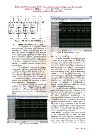
Figure 5: Regular 16-bit SQRT CSLA
IV. Basic Structure of Modified 16-Bit
CSLA
It is similar to regular 16-bit SQRT CSLA.
Only change is that in basic blocks having two
ripple-carry adders, one ripple carry adder fed with a
constant 1 carry-in is replaced by BEC. The area
estimation of each group is calculated.
Based on the consideration of delay values,
the arrival time of selection input C1 [time (T) =7]
of 6:3 mux is earlier than the s3 [t =9] and c3 [t =7]
and later than the s2 [t =4]. Thus, the sum3 and final
c3 (output from mux) are depending on s3 and mux
and partial c3 (input to mux) and mux, respectively.
The sum2 depends on c1 and mux. For the
remaining parts the arrival time of mux selection
input is always greater than the arrival time of data
inputs from the BEC’s. Thus, the delay of the
remaining MUX depends on the arrival time of mux
selection input and the mux delay.
First the coding for full adder and
multiplexers of 6:3, 8:4, 10:5, and 12:6 was done.
The BEC program was design by using NOT, XOR
and AND gates. Then 2, 3, 4, 5-bit ripple carry adder
was done by calling the full adder. The modified 16-
bit CSLA was created by calling the ripple carry
adders, BEC and all multiplexers based upon the
circuit. Finally, modified 64-bit was implemented in
the FIR filter design (section 5).
The arrival time of selection input of 6:3
mux is earlier. Thus, the sum3 and final c3 (output
from mux) depends on s3 and mux and partial c3
(input to mux) and mux, respectively. The sum2
depends on c1and mux. For the remaining group’s
the arrival time of mux selection input is always
greater than the arrival time of data inputs from the
BEC’s. Thus, the delay of the remaining groups
depends on the arrival time of mux selection input
and the mux delay.
4. B.Bharathi1
C.V.Subhaskar Reddy / International Journal of Engineering Research and
Applications (IJERA) ISSN: 2248-9622 www.ijera.com
Vol. 3, Issue 4, Jul-Aug 2013, pp. 437-441
440 | P a g e
Figure. 6. Modified 16-bit SQRT CSLA.
V. IMPLEMENTATION RESULTS
The design proposed in this paper has been
developed using Verilog-HDL and synthesized in
Xilinx ISE 9.1i. For each word size of the adder, the
same value changed dump (VCD) file is generated
for all possible input conditions and imported the
same to Xilinx ISE 9.1i Power Analysis to perform
the power simulations. The similar design flow is
followed for both the regular and modified SQRT
CSLA. Table 5 exhibits the simulation results of
both the CSLA fir filter structures in terms of delay,
area and power.
The power–delay product of the proposed
8-bit is higher than that of the regular SQRT CSLA
by 5.2% and the area-delay product is lower by
2.9%. However, the power-delay product of the
proposed 16-bit SQRT CSLA reduces by 1.76% and
for the 32-bit, 64-bit and by as much as 8.18%, and
12.28% respectively. input (a sequence of numbers,
resulting from sampling and quantizing an analog
signal) and produces a digital output.
The simulation Results of regular and
Modified Carry Select adder shown figure 7 and
8.comapre to regular CSLA modified CSLA
architecture is take less amount of delay it is
approximately reduced by 30% of regular method
design
Figure. 7. Regular 16-bit CSLA
Figure. 8. Modified 16-bit CSLA
VI. CONCLUSION
A simple approach is proposed in this paper
to reduce the area and power of SQRT CSLA
architecture. The reduced number of gates of this
work offers the great advantage in the reduction of
area and also the total power. The compared results
show that the modified SQRT CSLA has a slightly
larger delay (only3.76%), but the area and power of
the 128-bit modified SQRT CSLA are significantly
reduced by 17.4% and 15.4% respectively. The
power-delay product and also the area-delay product
of the proposed design show a decrease for 16, 32,64
and 128-bit sizes which indicates the success of the
method and not a mere tradeoff of delay for power
and area. The modified CSLA architecture is
therefore, low area, low power, simple and efficient
for VLSI hardware implementation.
As the functional verification decides the
quality of the silicon, we spend 60% of the design
cycle time only for the verification/simulation. In
order to avoid the delay and meet the TTM, we use
the latest verification methodologies and
technologies and accelerate the verification process.
This project helps one to understand the complete
functional verification process of complex ASICs an
SoC’s and it gives opportunity to try the latest
verification methodologies, programming concepts
like Object Oriented Programming of Hardware
Verification Languages and sophisticated EDA
tools, for the high quality verification.
Future Work: This project used System Verilog
i.e., the technology used is direct test cases,
randomized test cases ,OVM for verification even
though the coverage is 100% there may be some
errors which cannot be shown so in Oder to
overcome this the new technology of System
5. B.Bharathi1
C.V.Subhaskar Reddy / International Journal of Engineering Research and
Applications (IJERA) ISSN: 2248-9622 www.ijera.com
Vol. 3, Issue 4, Jul-Aug 2013, pp. 437-441
441 | P a g e
Verilog i.e., OVM and UVM. In the coming future
the Router can be done by using OVM and UVM.
REFERENCES
[1] Bedrij, O. J.,(1962), “Carry-select adder,”
IRE Trans. Electron. Comput., pp.340–344.
[2] Ceiang ,T. Y. and Hsiao,M. J. ,(Oct1998
),“Carry-select adder using single ripple
carry adder,” Electron. Lett., vol. 34, no.
22, pp. 2101– 2103
[3] He, Y. , Chang ,C. H. and Gu, J. , (2005),
“An A rea efficient 64-bit square root carry-
select adder for low power application,” in
Proc. IEEE Int. Symp.Circuits Syst. vol. 4,
pp. 4082–4085.
[4] Ramkumar,B. , Kittur, H.M. and Kannan
,P. M. ,(2010 ),“ASIC implementation of
modified faster carry save adder,” Eur. J.
Sci. Res., vol. 42, no. 1,pp.53–58.
[5] Kim ,Y. and Kim ,L.-S.,(May2001), “64-bit
carry-select adder with reduced
area,”Electron Lett., vol. 37, no. 10, pp.
614–615.
[6] E. Abu-Shama and M. Bayoumi, “A New
cell for low power adders,” in Proc.Int.
Midwest Symp. Circuits and Systems,
1995, pp. 1014–1017
[7] www.xilinx.com.
[8] Verilog HDL- Digital Design and
Synthesis, by Samir Palnitkar