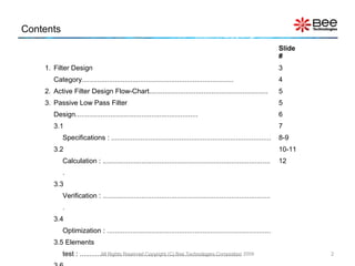
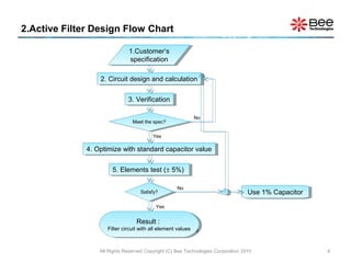
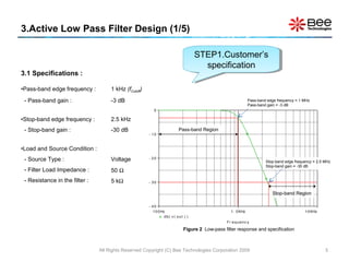
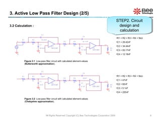
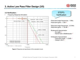
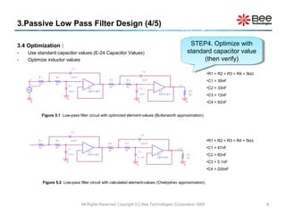
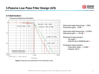
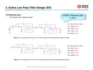
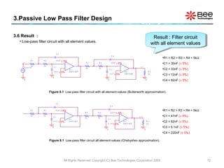
SlideShare a Scribd company logo
Active Filter Design
All Rights Reserved Copyright (C) Bee Technologies Corporation 2010 1
Design Services
Contents
Slide
#
1. Filter Design
Category..............................................................................
2. Active Filter Design Flow-Chart.............................................................
3. Passive Low Pass Filter
Design...............................................................
3.1
Specifications : ..................................................................................
3.2
Calculation : ......................................................................................
.
3.3
Verification : ......................................................................................
.
3.4
Optimization : ....................................................................................
3.5 Elements
test : ...................................................................................
3
4
5
5
6
7
8-9
10-11
12
2All Rights Reserved Copyright (C) Bee Technologies Corporation 2009
1.Filter Design Category
Available Filter Types
• Low Pass Filter
• High Pass Filter
• Band Pass Filter
• Band Reject Filter
Approximation
• Butterworth
- No ripple
- Smooth roll-off (rate of 20dB/decade for every pole)
• Chebyshev
- Pass-band ripple specification would be required.
- Steeper roll-of
Topology
• Passive
- High frequency range (> 1 MHz)
- Source and load impedance specifications would be required
• Active
- Low frequency range (1 Hz to 1 MHz)
- Unity-Gain Sallen-Key configuration (see Figure 1.0)
Number of Order
• 2nd
-10th
All Rights Reserved Copyright (C) Bee Technologies Corporation 2010 3
R 1 R 2
C 2
0
C 1
in
+
-
U 1
A M P S I M P
o u t
Fig.1.0 Unity-Gain Sallen-Key Active Filter (2nd
-Order Active LPF)
2.Active Filter Design Flow Chart
All Rights Reserved Copyright (C) Bee Technologies Corporation 2010 4
2. Circuit design and calculation2. Circuit design and calculation
3. Verification3. Verification
4. Optimize with standard capacitor value4. Optimize with standard capacitor value
5. Elements test (± 5%)5. Elements test (± 5%)
Meet the spec?Meet the spec?
No
Yes
Satisfy?Satisfy?
Yes
YESYES
Result :
Filter circuit with all element values
Result :
Filter circuit with all element values
Use 1% CapacitorUse 1% Capacitor
1.Customer’s
specification
1.Customer’s
specification
No
Fr equenc y
100Hz 1. 0KHz 10KHz
db( v ( out ) )
- 40
- 30
- 20
- 10
0
3.Active Low Pass Filter Design (1/5)
3.1 Specifications :
All Rights Reserved Copyright (C) Bee Technologies Corporation 2009 5
Figure 2 Low-pass filter response and specification
Pass-band Region
Stop-band Region
Pass-band edge frequency = 1 MHz
Pass-band gain = -3 dB
Stop-band edge frequency = 2.5 MHz
Stop-band gain = -30 dB
•Pass-band edge frequency : 1 kHz (fCutoff)
- Pass-band gain : -3 dB
•Stop-band edge frequency : 2.5 kHz
- Stop-band gain : -30 dB
•Load and Source Condition :
- Source Type : Voltage
- Filter Load Impedance : 50 Ω
- Resistance in the filter : 5 kΩ
STEP1.Customer’s
specification
STEP1.Customer’s
specification
R 1
5 k
R 2
5 k
R 5
5 0
0
C 1
2 9 . 4 2 n F
0
C 2
3 4 . 4 4 n F
R 3
5 k
R 4
5 k
C 3
1 2 . 1 8 n F
0
C 4
8 3 . 1 7 n F
+
-
U 2
A M P S I M P
o u tV s o u r c e
0
in
+
-
U 1
A M P S I M P
3. Active Low Pass Filter Design (2/5)
3.2 Calculation :
All Rights Reserved Copyright (C) Bee Technologies Corporation 2009 6
Figure 3.1 Low-pass filter circuit with calculated element-values
(Butterworth approximation).
Figure 3.2 Low-pass filter circuit with calculated element-values
(Chebyshev approximation).
•R1 = R2 = R3 = R4 = 5kΩ
•C1 = 29.42nF
•C2 = 34.44nF
•C3 = 83.17nF
•C4 = 12.18nF
STEP2. Circuit
design and
calculation
STEP2. Circuit
design and
calculation
•R1 = R2 = R3 = R4 = 5kΩ
•C1 = 47nF
•C2 = 82nF
•C3 = 5.1nF
•C4 = 220nF
R 1
5 k
R 2
5 k
R 5
5 0
0
C 1
4 7 n F
0
C 2
8 2 n F
R 3
5 k
R 4
5 k
0
C 3
5 . 1 n F
C 4
2 2 0 n F
+
-
U 3
A M P S I M P
o u t 2
+
-
U 4
A M P S I M P
Fr equenc y
100Hz 1. 0KHz 10KHz
db( v ( out ) ) db ( v ( out 2) )
- 60
- 40
- 20
- 0
3. Active Low Pass Filter Design (3/5)
All Rights Reserved Copyright (C) Bee Technologies Corporation 2009 7
Figure 4 Response and specification of the calculated circuits.
Butterworth (1MHz,-3.013dB)
Chebyshev : (1MHz,-2.818dB)
(2.5MHz,-44dB)
(2.5MHz,-31.858dB)
3.3 Verification :
• Frequency Response Simulation
Pass-band Ripple (-1.23dB) •Pass-band edge frequencies : 1 MHz
•Pass-band gains : -3 dB 
•Stop-band edge frequencies : 2.5 MHz
•Stop-band gains : < -30 dB 
•Butterworth Approximation
- No ripple 
- Roll-off rate is 80dB/decade 
•Chebyshev Approximation
- Pass-band ripple : -1.23dB 
- Steeper roll-of 
— Butterworth Approximation
STEP3.
Verification
STEP3.
Verification
3.4 Optimization :
- Use standard capacitor values (E-24 Capacitor Values)
- Optimize inductor values
R 1
5 k
R 2
5 k
R 5
5 0
0
C 1
3 0 n F
0
C 2
3 3 n F
R 3
5 k
R 4
5 k
C 3
1 2 n F
0
C 4
8 2 n F
+
-
U 2
A M P S I M P
o u tV s o u r c e
0
in
+
-
U 1
A M P S I M P
3.Passive Low Pass Filter Design (4/5)
All Rights Reserved Copyright (C) Bee Technologies Corporation 2009 8
Figure 5.1 Low-pass filter circuit with optimized element-values (Butterworth approximation).
Figure 5.2 Low-pass filter circuit with calculated element-values (Chebyshev approximation).
STEP4. Optimize with
standard capacitor value
(then verify)
STEP4. Optimize with
standard capacitor value
(then verify)
•R1 = R2 = R3 = R4 = 5kΩ
•C1 = 47nF
•C2 = 82nF
•C3 = 5.1nF
•C4 = 220nF
R 1
5 k
R 2
5 k
R 5
5 0
0
C 1
4 7 n F
0
C 2
8 2 n F
R 3
5 k
R 4
5 k
0
C 3
5 . 1 n F
C 4
2 2 0 n F
+
-
U 3
A M P S I M P
o u t 2
+
-
U 4
A M P S I M P
•R1 = R2 = R3 = R4 = 5kΩ
•C1 = 30nF
•C2 = 33nF
•C3 = 12nF
•C4 = 82nF
Fr equenc y
100Hz 1. 0KHz 10KHz
db( v ( out ) ) db ( v ( out 2) )
- 60
- 40
- 20
- 0
3.Passive Low Pass Filter Design (4/5)
All Rights Reserved Copyright (C) Bee Technologies Corporation 2009 9
Figure 6 Response and specification of the optimized circuits.
3.4 Optimization :
• Frequency Response Simulation
•Pass-band edge frequencies : 1 MHz
•Pass-band gains : -3 dB 
•Stop-band edge frequencies : 2.5 MHz
•Stop-band gains : < -30 dB 
•Butterworth Approximation
- No ripple 
- Roll-off rate is 80dB/decade 
•Chebyshev Approximation
- Pass-band ripple : -1.23dB 
- Steeper roll-of 
Butterworth (1MHz,-3.06dB)
Chebyshev : (1MHz,-2.818dB)
(2.5MHz,-44dB)
(2.5MHz,-31.521dB)
Pass-band Ripple (-1.23dB)
— Butterworth Approximation
3.5 Elements test :
- ± 5% test for each capacitor value.
R 1
5 k
R 2
5 k
R 5
5 0
0
C 1
4 7 n F
0
C 2
8 2 n F
R 3
5 k
R 4
5 k
0
C 3
5 . 1 n F
C 4
2 2 0 n F
+
-
U 3
A M P S I M P
o u t 2
+
-
U 4
A M P S I M P
R 1
5 k
R 2
5 k
R 5
5 0
0
C 1
3 0 n F
0
C 2
3 3 n F
R 3
5 k
R 4
5 k
C 3
1 2 n F
0
C 4
8 2 n F
+
-
U 2
A M P S I M P
o u tV s o u r c e
0
in
+
-
U 1
A M P S I M P
3. Active Low Pass Filter Design (5/5)
All Rights Reserved Copyright (C) Bee Technologies Corporation 2009 10
Figure 7.1 Low-pass filter circuit with ± 5% of the capacitance-values (Butterworth approximation).
Figure 7.1 Low-pass filter circuit with ± 5% of the capacitance-values (Chebyshev approximation).
STEP5. Elements test
(± 5%)
STEP5. Elements test
(± 5%)
•R1 = R2 = R3 = R4 = 5kΩ
•C1 = 47nF (± 5%)
•C2 = 82nF (± 5%)
•C3 = 5.1nF (± 5%)
•C4 = 220nF (± 5%)
•R1 = R2 = R3 = R4 = 5kΩ
•C1 = 30nF (± 5%)
•C2 = 33nF (± 5%)
•C3 = 12nF (± 5%)
•C4 = 82nF (± 5%)
Fr eque nc y
1 00Hz 1. 0KHz 1 0KHz
db( v ( o ut 2 ) )
- 6 0
- 4 0
- 2 0
- 0
Fr eq ue nc y
1 00 Hz 1. 0KHz 10 KHz
db ( v ( ou t ) )
- 60
- 40
- 20
- 0
3.Passive Low Pass Filter Design (5/5)
All Rights Reserved Copyright (C) Bee Technologies Corporation 2009 11
Figure 8 Response and specification when the element values are error with ±5%.
3.5 Elements test :
• Frequency Response Simulation, compare to -5% and +5% of all element values.
Butterworth
— +5%
— standard values
— -5%
Pass-band gain (-3 dB)
Cutoff frequency : 0.9486M, 1M, 1.0485M
Chebyshev
— +5%
— standard values
— -5%
Cutoff frequency : 0.9564M, 1M, 1.0567M
Pass-band gain (-3 dB)
R 1
5 k
R 2
5 k
R 5
5 0
0
C 1
4 7 n F
0
C 2
8 2 n F
R 3
5 k
R 4
5 k
0
C 3
5 . 1 n F
C 4
2 2 0 n F
+
-
U 3
A M P S I M P
o u t 2
+
-
U 4
A M P S I M P
R 1
5 k
R 2
5 k
R 5
5 0
0
C 1
3 0 n F
0
C 2
3 3 n F
R 3
5 k
R 4
5 k
C 3
1 2 n F
0
C 4
8 2 n F
+
-
U 2
A M P S I M P
o u tV s o u r c e
0
in
+
-
U 1
A M P S I M P
•R1 = R2 = R3 = R4 = 5kΩ
•C1 = 47nF (± 5%)
•C2 = 82nF (± 5%)
•C3 = 5.1nF (± 5%)
•C4 = 220nF (± 5%)
•R1 = R2 = R3 = R4 = 5kΩ
•C1 = 30nF (± 5%)
•C2 = 33nF (± 5%)
•C3 = 12nF (± 5%)
•C4 = 82nF (± 5%)
3.Passive Low Pass Filter Design
3.6 Result :
• Low-pass filter circuit with all element values.
All Rights Reserved Copyright (C) Bee Technologies Corporation 2009 12
Figure 8.1 Low-pass filter circuit with all element-values (Butterworth approximation).
Figure 8.1 Low-pass filter circuit all element-values (Chebyshev approximation).
± 5%
± 5%
± 5%
± 5%
± 5%
± 5%
± 5%
Result : Filter circuit
with all element values
Result : Filter circuit
with all element values
± 5%

More Related Content

What's hot

Fet biasing boylestad pages
Fet biasing boylestad pagesFet biasing boylestad pages
Fet biasing boylestad pagesLingalaSowjanya
 
Successive approximation adc
Successive approximation adcSuccessive approximation adc
Successive approximation adcMaria Roshan
 
Study of vco_Voltage controlled Oscillator
Study of vco_Voltage controlled OscillatorStudy of vco_Voltage controlled Oscillator
Study of vco_Voltage controlled OscillatorNeha Mannewar
 
Active inductor design new
Active inductor design newActive inductor design new
Active inductor design newDEVITH T
 
Phase-locked Loops - Theory and Design
Phase-locked Loops - Theory and DesignPhase-locked Loops - Theory and Design
Phase-locked Loops - Theory and DesignSimen Li
 
FM-Foster - Seeley Discriminator.pptx
FM-Foster - Seeley Discriminator.pptxFM-Foster - Seeley Discriminator.pptx
FM-Foster - Seeley Discriminator.pptxArunChokkalingam
 
Spectrum Analyzer Fundamentals/Advanced Spectrum Analysis
Spectrum Analyzer Fundamentals/Advanced Spectrum AnalysisSpectrum Analyzer Fundamentals/Advanced Spectrum Analysis
Spectrum Analyzer Fundamentals/Advanced Spectrum AnalysisRohde & Schwarz North America
 
Frequency synthesizers
Frequency  synthesizersFrequency  synthesizers
Frequency synthesizerssiva23143
 
RF Module Design - [Chapter 5] Low Noise Amplifier
RF Module Design - [Chapter 5]  Low Noise AmplifierRF Module Design - [Chapter 5]  Low Noise Amplifier
RF Module Design - [Chapter 5] Low Noise AmplifierSimen Li
 
Analog modulation
Analog modulationAnalog modulation
Analog modulationvish0110
 

What's hot (20)

Transistor 1 lecture
Transistor 1 lectureTransistor 1 lecture
Transistor 1 lecture
 
Successive approximation
Successive approximationSuccessive approximation
Successive approximation
 
Fet biasing boylestad pages
Fet biasing boylestad pagesFet biasing boylestad pages
Fet biasing boylestad pages
 
Active filters
Active filtersActive filters
Active filters
 
Impedance Matching
Impedance MatchingImpedance Matching
Impedance Matching
 
Successive approximation adc
Successive approximation adcSuccessive approximation adc
Successive approximation adc
 
Filtros
FiltrosFiltros
Filtros
 
Study of vco_Voltage controlled Oscillator
Study of vco_Voltage controlled OscillatorStudy of vco_Voltage controlled Oscillator
Study of vco_Voltage controlled Oscillator
 
Comm008 e4 maala
Comm008 e4 maalaComm008 e4 maala
Comm008 e4 maala
 
Active inductor design new
Active inductor design newActive inductor design new
Active inductor design new
 
Phase-locked Loops - Theory and Design
Phase-locked Loops - Theory and DesignPhase-locked Loops - Theory and Design
Phase-locked Loops - Theory and Design
 
Band pass filter
Band pass filterBand pass filter
Band pass filter
 
FM-Foster - Seeley Discriminator.pptx
FM-Foster - Seeley Discriminator.pptxFM-Foster - Seeley Discriminator.pptx
FM-Foster - Seeley Discriminator.pptx
 
Spectrum Analyzer Fundamentals/Advanced Spectrum Analysis
Spectrum Analyzer Fundamentals/Advanced Spectrum AnalysisSpectrum Analyzer Fundamentals/Advanced Spectrum Analysis
Spectrum Analyzer Fundamentals/Advanced Spectrum Analysis
 
Frequency synthesizers
Frequency  synthesizersFrequency  synthesizers
Frequency synthesizers
 
Oscillators
OscillatorsOscillators
Oscillators
 
RF Module Design - [Chapter 5] Low Noise Amplifier
RF Module Design - [Chapter 5]  Low Noise AmplifierRF Module Design - [Chapter 5]  Low Noise Amplifier
RF Module Design - [Chapter 5] Low Noise Amplifier
 
Mosfet
MosfetMosfet
Mosfet
 
Analog modulation
Analog modulationAnalog modulation
Analog modulation
 
PA linearity
PA linearityPA linearity
PA linearity
 

Similar to Active Filter Design Using PSpice

Lect2 up400 (100329)
Lect2 up400 (100329)Lect2 up400 (100329)
Lect2 up400 (100329)aicdesign
 
Introduction to Memory Effects
Introduction to Memory EffectsIntroduction to Memory Effects
Introduction to Memory EffectsSohail Khanifar
 
Presentació renovables
Presentació renovablesPresentació renovables
Presentació renovablesJordi Cusido
 
RF Module Design - [Chapter 8] Phase-Locked Loops
RF Module Design - [Chapter 8] Phase-Locked LoopsRF Module Design - [Chapter 8] Phase-Locked Loops
RF Module Design - [Chapter 8] Phase-Locked LoopsSimen Li
 
MagneTag Presentation Winter Quarter V3.0
MagneTag Presentation Winter Quarter V3.0MagneTag Presentation Winter Quarter V3.0
MagneTag Presentation Winter Quarter V3.0John-Paul Petersen
 
RM03D-3_DCOBISC_06_07_09_Final
RM03D-3_DCOBISC_06_07_09_FinalRM03D-3_DCOBISC_06_07_09_Final
RM03D-3_DCOBISC_06_07_09_Finalimranbashir
 
All Digital Phase Lock Loop 03 12 09
All Digital Phase Lock Loop 03 12 09All Digital Phase Lock Loop 03 12 09
All Digital Phase Lock Loop 03 12 09imranbashir
 
Analog RF Front End Architecture
Analog RF Front End ArchitectureAnalog RF Front End Architecture
Analog RF Front End ArchitectureSHIV DUTT
 
Real 2nd order LC PLL loop analysis.pptx
Real 2nd order LC PLL loop analysis.pptxReal 2nd order LC PLL loop analysis.pptx
Real 2nd order LC PLL loop analysis.pptxSaiGouthamSunkara
 

Similar to Active Filter Design Using PSpice (20)

AD8351.pdf
AD8351.pdfAD8351.pdf
AD8351.pdf
 
Lect2 up400 (100329)
Lect2 up400 (100329)Lect2 up400 (100329)
Lect2 up400 (100329)
 
Butterworth filter
Butterworth filterButterworth filter
Butterworth filter
 
Introduction to Memory Effects
Introduction to Memory EffectsIntroduction to Memory Effects
Introduction to Memory Effects
 
Presentació renovables
Presentació renovablesPresentació renovables
Presentació renovables
 
RF Module Design - [Chapter 8] Phase-Locked Loops
RF Module Design - [Chapter 8] Phase-Locked LoopsRF Module Design - [Chapter 8] Phase-Locked Loops
RF Module Design - [Chapter 8] Phase-Locked Loops
 
Exp passive filter (6)
Exp passive filter (6)Exp passive filter (6)
Exp passive filter (6)
 
MagneTag Presentation Winter Quarter V3.0
MagneTag Presentation Winter Quarter V3.0MagneTag Presentation Winter Quarter V3.0
MagneTag Presentation Winter Quarter V3.0
 
Exp passive filter (9)
Exp passive filter (9)Exp passive filter (9)
Exp passive filter (9)
 
RM03D-3_DCOBISC_06_07_09_Final
RM03D-3_DCOBISC_06_07_09_FinalRM03D-3_DCOBISC_06_07_09_Final
RM03D-3_DCOBISC_06_07_09_Final
 
Exp passive filter (5)
Exp passive filter (5)Exp passive filter (5)
Exp passive filter (5)
 
All Digital Phase Lock Loop 03 12 09
All Digital Phase Lock Loop 03 12 09All Digital Phase Lock Loop 03 12 09
All Digital Phase Lock Loop 03 12 09
 
Analog RF Front End Architecture
Analog RF Front End ArchitectureAnalog RF Front End Architecture
Analog RF Front End Architecture
 
Exp passive filter (3)
Exp passive filter (3)Exp passive filter (3)
Exp passive filter (3)
 
11750882_01.PDF
11750882_01.PDF11750882_01.PDF
11750882_01.PDF
 
Real 2nd order LC PLL loop analysis.pptx
Real 2nd order LC PLL loop analysis.pptxReal 2nd order LC PLL loop analysis.pptx
Real 2nd order LC PLL loop analysis.pptx
 
16971168.ppt
16971168.ppt16971168.ppt
16971168.ppt
 
Active filters
Active filtersActive filters
Active filters
 
Exp passive filter (7)
Exp passive filter (7)Exp passive filter (7)
Exp passive filter (7)
 
Ad7716
Ad7716Ad7716
Ad7716
 

More from Tsuyoshi Horigome

FedExで書類を送付する場合の設定について(オンライン受付にて登録する場合について)
FedExで書類を送付する場合の設定について(オンライン受付にて登録する場合について)FedExで書類を送付する場合の設定について(オンライン受付にて登録する場合について)
FedExで書類を送付する場合の設定について(オンライン受付にて登録する場合について)Tsuyoshi Horigome
 
Update 46 models(Solar Cell) in SPICE PARK(MAY2024)
Update 46 models(Solar Cell) in SPICE PARK(MAY2024)Update 46 models(Solar Cell) in SPICE PARK(MAY2024)
Update 46 models(Solar Cell) in SPICE PARK(MAY2024)Tsuyoshi Horigome
 
SPICE PARK APR2024 ( 6,793 SPICE Models )
SPICE PARK APR2024 ( 6,793 SPICE Models )SPICE PARK APR2024 ( 6,793 SPICE Models )
SPICE PARK APR2024 ( 6,793 SPICE Models )Tsuyoshi Horigome
 
Update 22 models(Schottky Rectifier ) in SPICE PARK(APR2024)
Update 22 models(Schottky Rectifier ) in SPICE PARK(APR2024)Update 22 models(Schottky Rectifier ) in SPICE PARK(APR2024)
Update 22 models(Schottky Rectifier ) in SPICE PARK(APR2024)Tsuyoshi Horigome
 
SPICE PARK APR2024 ( 6,747 SPICE Models )
SPICE PARK APR2024 ( 6,747 SPICE Models )SPICE PARK APR2024 ( 6,747 SPICE Models )
SPICE PARK APR2024 ( 6,747 SPICE Models )Tsuyoshi Horigome
 
Update 31 models(Diode/General ) in SPICE PARK(MAR2024)
Update 31 models(Diode/General ) in SPICE PARK(MAR2024)Update 31 models(Diode/General ) in SPICE PARK(MAR2024)
Update 31 models(Diode/General ) in SPICE PARK(MAR2024)Tsuyoshi Horigome
 
SPICE PARK MAR2024 ( 6,725 SPICE Models )
SPICE PARK MAR2024 ( 6,725 SPICE Models )SPICE PARK MAR2024 ( 6,725 SPICE Models )
SPICE PARK MAR2024 ( 6,725 SPICE Models )Tsuyoshi Horigome
 
Update 29 models(Solar cell) in SPICE PARK(FEB2024)
Update 29 models(Solar cell) in SPICE PARK(FEB2024)Update 29 models(Solar cell) in SPICE PARK(FEB2024)
Update 29 models(Solar cell) in SPICE PARK(FEB2024)Tsuyoshi Horigome
 
SPICE PARK FEB2024 ( 6,694 SPICE Models )
SPICE PARK FEB2024 ( 6,694 SPICE Models )SPICE PARK FEB2024 ( 6,694 SPICE Models )
SPICE PARK FEB2024 ( 6,694 SPICE Models )Tsuyoshi Horigome
 
Circuit simulation using LTspice(Case study)
Circuit simulation using LTspice(Case study)Circuit simulation using LTspice(Case study)
Circuit simulation using LTspice(Case study)Tsuyoshi Horigome
 
Mindmap of Semiconductor sales business(15FEB2024)
Mindmap of Semiconductor sales business(15FEB2024)Mindmap of Semiconductor sales business(15FEB2024)
Mindmap of Semiconductor sales business(15FEB2024)Tsuyoshi Horigome
 
2-STAGE COCKCROFT-WALTON [SCHEMATIC] using LTspice
2-STAGE COCKCROFT-WALTON [SCHEMATIC] using LTspice2-STAGE COCKCROFT-WALTON [SCHEMATIC] using LTspice
2-STAGE COCKCROFT-WALTON [SCHEMATIC] using LTspiceTsuyoshi Horigome
 
PSpice simulation of power supply for TI is Error
PSpice simulation of power supply  for TI is ErrorPSpice simulation of power supply  for TI is Error
PSpice simulation of power supply for TI is ErrorTsuyoshi Horigome
 
IGBT Simulation of Results from Rgext or Rgint
IGBT Simulation of Results from Rgext or RgintIGBT Simulation of Results from Rgext or Rgint
IGBT Simulation of Results from Rgext or RgintTsuyoshi Horigome
 
Electronic component sales method centered on alternative proposals
Electronic component sales method centered on alternative proposalsElectronic component sales method centered on alternative proposals
Electronic component sales method centered on alternative proposalsTsuyoshi Horigome
 
Electronic component sales method focused on new hires
Electronic component sales method focused on new hiresElectronic component sales method focused on new hires
Electronic component sales method focused on new hiresTsuyoshi Horigome
 
Mindmap(electronics parts sales visions)
Mindmap(electronics parts sales visions)Mindmap(electronics parts sales visions)
Mindmap(electronics parts sales visions)Tsuyoshi Horigome
 
Chat GPTによる伝達関数の導出
Chat GPTによる伝達関数の導出Chat GPTによる伝達関数の導出
Chat GPTによる伝達関数の導出Tsuyoshi Horigome
 
伝達関数の理解(Chatgpt)
伝達関数の理解(Chatgpt)伝達関数の理解(Chatgpt)
伝達関数の理解(Chatgpt)Tsuyoshi Horigome
 
DXセミナー(2024年1月17日開催)のメモ
DXセミナー(2024年1月17日開催)のメモDXセミナー(2024年1月17日開催)のメモ
DXセミナー(2024年1月17日開催)のメモTsuyoshi Horigome
 

More from Tsuyoshi Horigome (20)

FedExで書類を送付する場合の設定について(オンライン受付にて登録する場合について)
FedExで書類を送付する場合の設定について(オンライン受付にて登録する場合について)FedExで書類を送付する場合の設定について(オンライン受付にて登録する場合について)
FedExで書類を送付する場合の設定について(オンライン受付にて登録する場合について)
 
Update 46 models(Solar Cell) in SPICE PARK(MAY2024)
Update 46 models(Solar Cell) in SPICE PARK(MAY2024)Update 46 models(Solar Cell) in SPICE PARK(MAY2024)
Update 46 models(Solar Cell) in SPICE PARK(MAY2024)
 
SPICE PARK APR2024 ( 6,793 SPICE Models )
SPICE PARK APR2024 ( 6,793 SPICE Models )SPICE PARK APR2024 ( 6,793 SPICE Models )
SPICE PARK APR2024 ( 6,793 SPICE Models )
 
Update 22 models(Schottky Rectifier ) in SPICE PARK(APR2024)
Update 22 models(Schottky Rectifier ) in SPICE PARK(APR2024)Update 22 models(Schottky Rectifier ) in SPICE PARK(APR2024)
Update 22 models(Schottky Rectifier ) in SPICE PARK(APR2024)
 
SPICE PARK APR2024 ( 6,747 SPICE Models )
SPICE PARK APR2024 ( 6,747 SPICE Models )SPICE PARK APR2024 ( 6,747 SPICE Models )
SPICE PARK APR2024 ( 6,747 SPICE Models )
 
Update 31 models(Diode/General ) in SPICE PARK(MAR2024)
Update 31 models(Diode/General ) in SPICE PARK(MAR2024)Update 31 models(Diode/General ) in SPICE PARK(MAR2024)
Update 31 models(Diode/General ) in SPICE PARK(MAR2024)
 
SPICE PARK MAR2024 ( 6,725 SPICE Models )
SPICE PARK MAR2024 ( 6,725 SPICE Models )SPICE PARK MAR2024 ( 6,725 SPICE Models )
SPICE PARK MAR2024 ( 6,725 SPICE Models )
 
Update 29 models(Solar cell) in SPICE PARK(FEB2024)
Update 29 models(Solar cell) in SPICE PARK(FEB2024)Update 29 models(Solar cell) in SPICE PARK(FEB2024)
Update 29 models(Solar cell) in SPICE PARK(FEB2024)
 
SPICE PARK FEB2024 ( 6,694 SPICE Models )
SPICE PARK FEB2024 ( 6,694 SPICE Models )SPICE PARK FEB2024 ( 6,694 SPICE Models )
SPICE PARK FEB2024 ( 6,694 SPICE Models )
 
Circuit simulation using LTspice(Case study)
Circuit simulation using LTspice(Case study)Circuit simulation using LTspice(Case study)
Circuit simulation using LTspice(Case study)
 
Mindmap of Semiconductor sales business(15FEB2024)
Mindmap of Semiconductor sales business(15FEB2024)Mindmap of Semiconductor sales business(15FEB2024)
Mindmap of Semiconductor sales business(15FEB2024)
 
2-STAGE COCKCROFT-WALTON [SCHEMATIC] using LTspice
2-STAGE COCKCROFT-WALTON [SCHEMATIC] using LTspice2-STAGE COCKCROFT-WALTON [SCHEMATIC] using LTspice
2-STAGE COCKCROFT-WALTON [SCHEMATIC] using LTspice
 
PSpice simulation of power supply for TI is Error
PSpice simulation of power supply  for TI is ErrorPSpice simulation of power supply  for TI is Error
PSpice simulation of power supply for TI is Error
 
IGBT Simulation of Results from Rgext or Rgint
IGBT Simulation of Results from Rgext or RgintIGBT Simulation of Results from Rgext or Rgint
IGBT Simulation of Results from Rgext or Rgint
 
Electronic component sales method centered on alternative proposals
Electronic component sales method centered on alternative proposalsElectronic component sales method centered on alternative proposals
Electronic component sales method centered on alternative proposals
 
Electronic component sales method focused on new hires
Electronic component sales method focused on new hiresElectronic component sales method focused on new hires
Electronic component sales method focused on new hires
 
Mindmap(electronics parts sales visions)
Mindmap(electronics parts sales visions)Mindmap(electronics parts sales visions)
Mindmap(electronics parts sales visions)
 
Chat GPTによる伝達関数の導出
Chat GPTによる伝達関数の導出Chat GPTによる伝達関数の導出
Chat GPTによる伝達関数の導出
 
伝達関数の理解(Chatgpt)
伝達関数の理解(Chatgpt)伝達関数の理解(Chatgpt)
伝達関数の理解(Chatgpt)
 
DXセミナー(2024年1月17日開催)のメモ
DXセミナー(2024年1月17日開催)のメモDXセミナー(2024年1月17日開催)のメモ
DXセミナー(2024年1月17日開催)のメモ
 

Recently uploaded

Expert Accessory Dwelling Unit (ADU) Drafting Services
Expert Accessory Dwelling Unit (ADU) Drafting ServicesExpert Accessory Dwelling Unit (ADU) Drafting Services
Expert Accessory Dwelling Unit (ADU) Drafting ServicesResDraft
 
Common Designing Mistakes and How to avoid them
Common Designing Mistakes and How to avoid themCommon Designing Mistakes and How to avoid them
Common Designing Mistakes and How to avoid themmadhavlakhanpal29
 
The Evolution of Fashion Trends: History to Fashion
The Evolution of Fashion Trends: History to FashionThe Evolution of Fashion Trends: History to Fashion
The Evolution of Fashion Trends: History to FashionPixel poets
 
National-Learning-Camp 2024 deped....pptx
National-Learning-Camp 2024 deped....pptxNational-Learning-Camp 2024 deped....pptx
National-Learning-Camp 2024 deped....pptxAlecAnidul
 
CA OFFICE office office office _VIEWS.pdf
CA OFFICE office office office _VIEWS.pdfCA OFFICE office office office _VIEWS.pdf
CA OFFICE office office office _VIEWS.pdfSudhanshuMandlik
 
Book Formatting: Quality Control Checks for Designers
Book Formatting: Quality Control Checks for DesignersBook Formatting: Quality Control Checks for Designers
Book Formatting: Quality Control Checks for DesignersConfidence Ago
 
Top 5 Indian Style Modular Kitchen Designs
Top 5 Indian Style Modular Kitchen DesignsTop 5 Indian Style Modular Kitchen Designs
Top 5 Indian Style Modular Kitchen DesignsFinzo Kitchens
 
Transforming Brand Perception and Boosting Profitability
Transforming Brand Perception and Boosting ProfitabilityTransforming Brand Perception and Boosting Profitability
Transforming Brand Perception and Boosting Profitabilityaaryangarg12
 
PORTFOLIO FABIANA VILLANI ARCHITECTURE.pdf
PORTFOLIO FABIANA VILLANI ARCHITECTURE.pdfPORTFOLIO FABIANA VILLANI ARCHITECTURE.pdf
PORTFOLIO FABIANA VILLANI ARCHITECTURE.pdffabianavillanib
 
Art Nouveau Movement Presentation for Art History.
Art Nouveau Movement Presentation for Art History.Art Nouveau Movement Presentation for Art History.
Art Nouveau Movement Presentation for Art History.rrimika1
 
The Design Code Google Developer Student Club.pptx
The Design Code Google Developer Student Club.pptxThe Design Code Google Developer Student Club.pptx
The Design Code Google Developer Student Club.pptxadityakushalsaha
 

Recently uploaded (11)

Expert Accessory Dwelling Unit (ADU) Drafting Services
Expert Accessory Dwelling Unit (ADU) Drafting ServicesExpert Accessory Dwelling Unit (ADU) Drafting Services
Expert Accessory Dwelling Unit (ADU) Drafting Services
 
Common Designing Mistakes and How to avoid them
Common Designing Mistakes and How to avoid themCommon Designing Mistakes and How to avoid them
Common Designing Mistakes and How to avoid them
 
The Evolution of Fashion Trends: History to Fashion
The Evolution of Fashion Trends: History to FashionThe Evolution of Fashion Trends: History to Fashion
The Evolution of Fashion Trends: History to Fashion
 
National-Learning-Camp 2024 deped....pptx
National-Learning-Camp 2024 deped....pptxNational-Learning-Camp 2024 deped....pptx
National-Learning-Camp 2024 deped....pptx
 
CA OFFICE office office office _VIEWS.pdf
CA OFFICE office office office _VIEWS.pdfCA OFFICE office office office _VIEWS.pdf
CA OFFICE office office office _VIEWS.pdf
 
Book Formatting: Quality Control Checks for Designers
Book Formatting: Quality Control Checks for DesignersBook Formatting: Quality Control Checks for Designers
Book Formatting: Quality Control Checks for Designers
 
Top 5 Indian Style Modular Kitchen Designs
Top 5 Indian Style Modular Kitchen DesignsTop 5 Indian Style Modular Kitchen Designs
Top 5 Indian Style Modular Kitchen Designs
 
Transforming Brand Perception and Boosting Profitability
Transforming Brand Perception and Boosting ProfitabilityTransforming Brand Perception and Boosting Profitability
Transforming Brand Perception and Boosting Profitability
 
PORTFOLIO FABIANA VILLANI ARCHITECTURE.pdf
PORTFOLIO FABIANA VILLANI ARCHITECTURE.pdfPORTFOLIO FABIANA VILLANI ARCHITECTURE.pdf
PORTFOLIO FABIANA VILLANI ARCHITECTURE.pdf
 
Art Nouveau Movement Presentation for Art History.
Art Nouveau Movement Presentation for Art History.Art Nouveau Movement Presentation for Art History.
Art Nouveau Movement Presentation for Art History.
 
The Design Code Google Developer Student Club.pptx
The Design Code Google Developer Student Club.pptxThe Design Code Google Developer Student Club.pptx
The Design Code Google Developer Student Club.pptx
 

Active Filter Design Using PSpice

  • 1. Active Filter Design All Rights Reserved Copyright (C) Bee Technologies Corporation 2010 1 Design Services
  • 2. Contents Slide # 1. Filter Design Category.............................................................................. 2. Active Filter Design Flow-Chart............................................................. 3. Passive Low Pass Filter Design............................................................... 3.1 Specifications : .................................................................................. 3.2 Calculation : ...................................................................................... . 3.3 Verification : ...................................................................................... . 3.4 Optimization : .................................................................................... 3.5 Elements test : ................................................................................... 3 4 5 5 6 7 8-9 10-11 12 2All Rights Reserved Copyright (C) Bee Technologies Corporation 2009
  • 3. 1.Filter Design Category Available Filter Types • Low Pass Filter • High Pass Filter • Band Pass Filter • Band Reject Filter Approximation • Butterworth - No ripple - Smooth roll-off (rate of 20dB/decade for every pole) • Chebyshev - Pass-band ripple specification would be required. - Steeper roll-of Topology • Passive - High frequency range (> 1 MHz) - Source and load impedance specifications would be required • Active - Low frequency range (1 Hz to 1 MHz) - Unity-Gain Sallen-Key configuration (see Figure 1.0) Number of Order • 2nd -10th All Rights Reserved Copyright (C) Bee Technologies Corporation 2010 3 R 1 R 2 C 2 0 C 1 in + - U 1 A M P S I M P o u t Fig.1.0 Unity-Gain Sallen-Key Active Filter (2nd -Order Active LPF)
  • 4. 2.Active Filter Design Flow Chart All Rights Reserved Copyright (C) Bee Technologies Corporation 2010 4 2. Circuit design and calculation2. Circuit design and calculation 3. Verification3. Verification 4. Optimize with standard capacitor value4. Optimize with standard capacitor value 5. Elements test (± 5%)5. Elements test (± 5%) Meet the spec?Meet the spec? No Yes Satisfy?Satisfy? Yes YESYES Result : Filter circuit with all element values Result : Filter circuit with all element values Use 1% CapacitorUse 1% Capacitor 1.Customer’s specification 1.Customer’s specification No
  • 5. Fr equenc y 100Hz 1. 0KHz 10KHz db( v ( out ) ) - 40 - 30 - 20 - 10 0 3.Active Low Pass Filter Design (1/5) 3.1 Specifications : All Rights Reserved Copyright (C) Bee Technologies Corporation 2009 5 Figure 2 Low-pass filter response and specification Pass-band Region Stop-band Region Pass-band edge frequency = 1 MHz Pass-band gain = -3 dB Stop-band edge frequency = 2.5 MHz Stop-band gain = -30 dB •Pass-band edge frequency : 1 kHz (fCutoff) - Pass-band gain : -3 dB •Stop-band edge frequency : 2.5 kHz - Stop-band gain : -30 dB •Load and Source Condition : - Source Type : Voltage - Filter Load Impedance : 50 Ω - Resistance in the filter : 5 kΩ STEP1.Customer’s specification STEP1.Customer’s specification
  • 6. R 1 5 k R 2 5 k R 5 5 0 0 C 1 2 9 . 4 2 n F 0 C 2 3 4 . 4 4 n F R 3 5 k R 4 5 k C 3 1 2 . 1 8 n F 0 C 4 8 3 . 1 7 n F + - U 2 A M P S I M P o u tV s o u r c e 0 in + - U 1 A M P S I M P 3. Active Low Pass Filter Design (2/5) 3.2 Calculation : All Rights Reserved Copyright (C) Bee Technologies Corporation 2009 6 Figure 3.1 Low-pass filter circuit with calculated element-values (Butterworth approximation). Figure 3.2 Low-pass filter circuit with calculated element-values (Chebyshev approximation). •R1 = R2 = R3 = R4 = 5kΩ •C1 = 29.42nF •C2 = 34.44nF •C3 = 83.17nF •C4 = 12.18nF STEP2. Circuit design and calculation STEP2. Circuit design and calculation •R1 = R2 = R3 = R4 = 5kΩ •C1 = 47nF •C2 = 82nF •C3 = 5.1nF •C4 = 220nF R 1 5 k R 2 5 k R 5 5 0 0 C 1 4 7 n F 0 C 2 8 2 n F R 3 5 k R 4 5 k 0 C 3 5 . 1 n F C 4 2 2 0 n F + - U 3 A M P S I M P o u t 2 + - U 4 A M P S I M P
  • 7. Fr equenc y 100Hz 1. 0KHz 10KHz db( v ( out ) ) db ( v ( out 2) ) - 60 - 40 - 20 - 0 3. Active Low Pass Filter Design (3/5) All Rights Reserved Copyright (C) Bee Technologies Corporation 2009 7 Figure 4 Response and specification of the calculated circuits. Butterworth (1MHz,-3.013dB) Chebyshev : (1MHz,-2.818dB) (2.5MHz,-44dB) (2.5MHz,-31.858dB) 3.3 Verification : • Frequency Response Simulation Pass-band Ripple (-1.23dB) •Pass-band edge frequencies : 1 MHz •Pass-band gains : -3 dB  •Stop-band edge frequencies : 2.5 MHz •Stop-band gains : < -30 dB  •Butterworth Approximation - No ripple  - Roll-off rate is 80dB/decade  •Chebyshev Approximation - Pass-band ripple : -1.23dB  - Steeper roll-of  — Butterworth Approximation — Butterworth Approximation STEP3. Verification STEP3. Verification
  • 8. 3.4 Optimization : - Use standard capacitor values (E-24 Capacitor Values) - Optimize inductor values R 1 5 k R 2 5 k R 5 5 0 0 C 1 3 0 n F 0 C 2 3 3 n F R 3 5 k R 4 5 k C 3 1 2 n F 0 C 4 8 2 n F + - U 2 A M P S I M P o u tV s o u r c e 0 in + - U 1 A M P S I M P 3.Passive Low Pass Filter Design (4/5) All Rights Reserved Copyright (C) Bee Technologies Corporation 2009 8 Figure 5.1 Low-pass filter circuit with optimized element-values (Butterworth approximation). Figure 5.2 Low-pass filter circuit with calculated element-values (Chebyshev approximation). STEP4. Optimize with standard capacitor value (then verify) STEP4. Optimize with standard capacitor value (then verify) •R1 = R2 = R3 = R4 = 5kΩ •C1 = 47nF •C2 = 82nF •C3 = 5.1nF •C4 = 220nF R 1 5 k R 2 5 k R 5 5 0 0 C 1 4 7 n F 0 C 2 8 2 n F R 3 5 k R 4 5 k 0 C 3 5 . 1 n F C 4 2 2 0 n F + - U 3 A M P S I M P o u t 2 + - U 4 A M P S I M P •R1 = R2 = R3 = R4 = 5kΩ •C1 = 30nF •C2 = 33nF •C3 = 12nF •C4 = 82nF
  • 9. Fr equenc y 100Hz 1. 0KHz 10KHz db( v ( out ) ) db ( v ( out 2) ) - 60 - 40 - 20 - 0 3.Passive Low Pass Filter Design (4/5) All Rights Reserved Copyright (C) Bee Technologies Corporation 2009 9 Figure 6 Response and specification of the optimized circuits. 3.4 Optimization : • Frequency Response Simulation •Pass-band edge frequencies : 1 MHz •Pass-band gains : -3 dB  •Stop-band edge frequencies : 2.5 MHz •Stop-band gains : < -30 dB  •Butterworth Approximation - No ripple  - Roll-off rate is 80dB/decade  •Chebyshev Approximation - Pass-band ripple : -1.23dB  - Steeper roll-of  Butterworth (1MHz,-3.06dB) Chebyshev : (1MHz,-2.818dB) (2.5MHz,-44dB) (2.5MHz,-31.521dB) Pass-band Ripple (-1.23dB) — Butterworth Approximation — Butterworth Approximation
  • 10. 3.5 Elements test : - ± 5% test for each capacitor value. R 1 5 k R 2 5 k R 5 5 0 0 C 1 4 7 n F 0 C 2 8 2 n F R 3 5 k R 4 5 k 0 C 3 5 . 1 n F C 4 2 2 0 n F + - U 3 A M P S I M P o u t 2 + - U 4 A M P S I M P R 1 5 k R 2 5 k R 5 5 0 0 C 1 3 0 n F 0 C 2 3 3 n F R 3 5 k R 4 5 k C 3 1 2 n F 0 C 4 8 2 n F + - U 2 A M P S I M P o u tV s o u r c e 0 in + - U 1 A M P S I M P 3. Active Low Pass Filter Design (5/5) All Rights Reserved Copyright (C) Bee Technologies Corporation 2009 10 Figure 7.1 Low-pass filter circuit with ± 5% of the capacitance-values (Butterworth approximation). Figure 7.1 Low-pass filter circuit with ± 5% of the capacitance-values (Chebyshev approximation). STEP5. Elements test (± 5%) STEP5. Elements test (± 5%) •R1 = R2 = R3 = R4 = 5kΩ •C1 = 47nF (± 5%) •C2 = 82nF (± 5%) •C3 = 5.1nF (± 5%) •C4 = 220nF (± 5%) •R1 = R2 = R3 = R4 = 5kΩ •C1 = 30nF (± 5%) •C2 = 33nF (± 5%) •C3 = 12nF (± 5%) •C4 = 82nF (± 5%)
  • 11. Fr eque nc y 1 00Hz 1. 0KHz 1 0KHz db( v ( o ut 2 ) ) - 6 0 - 4 0 - 2 0 - 0 Fr eq ue nc y 1 00 Hz 1. 0KHz 10 KHz db ( v ( ou t ) ) - 60 - 40 - 20 - 0 3.Passive Low Pass Filter Design (5/5) All Rights Reserved Copyright (C) Bee Technologies Corporation 2009 11 Figure 8 Response and specification when the element values are error with ±5%. 3.5 Elements test : • Frequency Response Simulation, compare to -5% and +5% of all element values. Butterworth — +5% — standard values — -5% Pass-band gain (-3 dB) Cutoff frequency : 0.9486M, 1M, 1.0485M Chebyshev — +5% — standard values — -5% Cutoff frequency : 0.9564M, 1M, 1.0567M Pass-band gain (-3 dB)
  • 12. R 1 5 k R 2 5 k R 5 5 0 0 C 1 4 7 n F 0 C 2 8 2 n F R 3 5 k R 4 5 k 0 C 3 5 . 1 n F C 4 2 2 0 n F + - U 3 A M P S I M P o u t 2 + - U 4 A M P S I M P R 1 5 k R 2 5 k R 5 5 0 0 C 1 3 0 n F 0 C 2 3 3 n F R 3 5 k R 4 5 k C 3 1 2 n F 0 C 4 8 2 n F + - U 2 A M P S I M P o u tV s o u r c e 0 in + - U 1 A M P S I M P •R1 = R2 = R3 = R4 = 5kΩ •C1 = 47nF (± 5%) •C2 = 82nF (± 5%) •C3 = 5.1nF (± 5%) •C4 = 220nF (± 5%) •R1 = R2 = R3 = R4 = 5kΩ •C1 = 30nF (± 5%) •C2 = 33nF (± 5%) •C3 = 12nF (± 5%) •C4 = 82nF (± 5%) 3.Passive Low Pass Filter Design 3.6 Result : • Low-pass filter circuit with all element values. All Rights Reserved Copyright (C) Bee Technologies Corporation 2009 12 Figure 8.1 Low-pass filter circuit with all element-values (Butterworth approximation). Figure 8.1 Low-pass filter circuit all element-values (Chebyshev approximation). ± 5% ± 5% ± 5% ± 5% ± 5% ± 5% ± 5% Result : Filter circuit with all element values Result : Filter circuit with all element values ± 5%