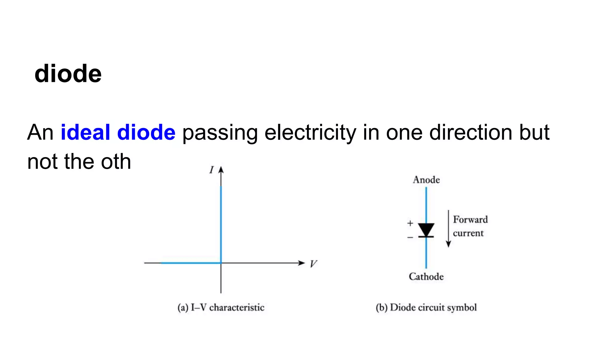
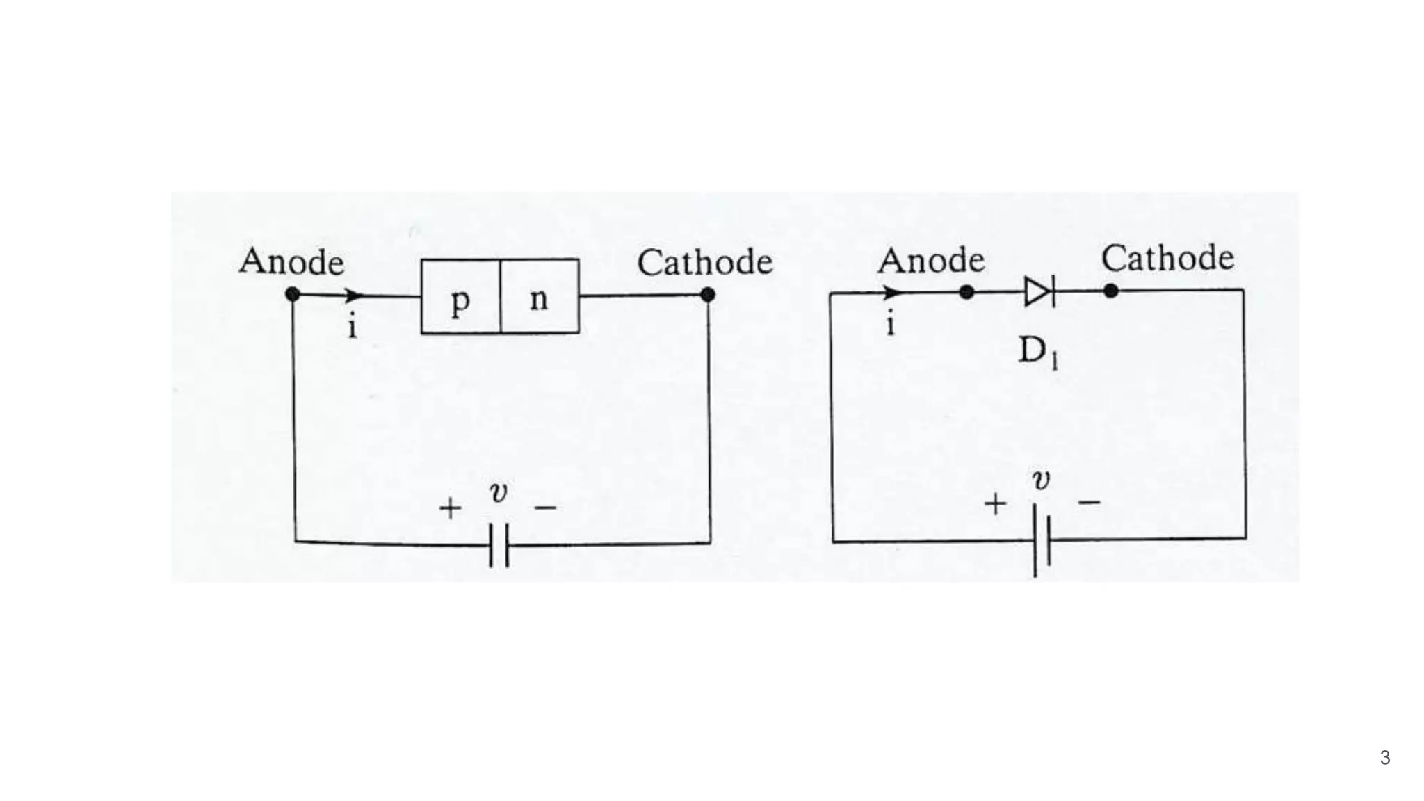
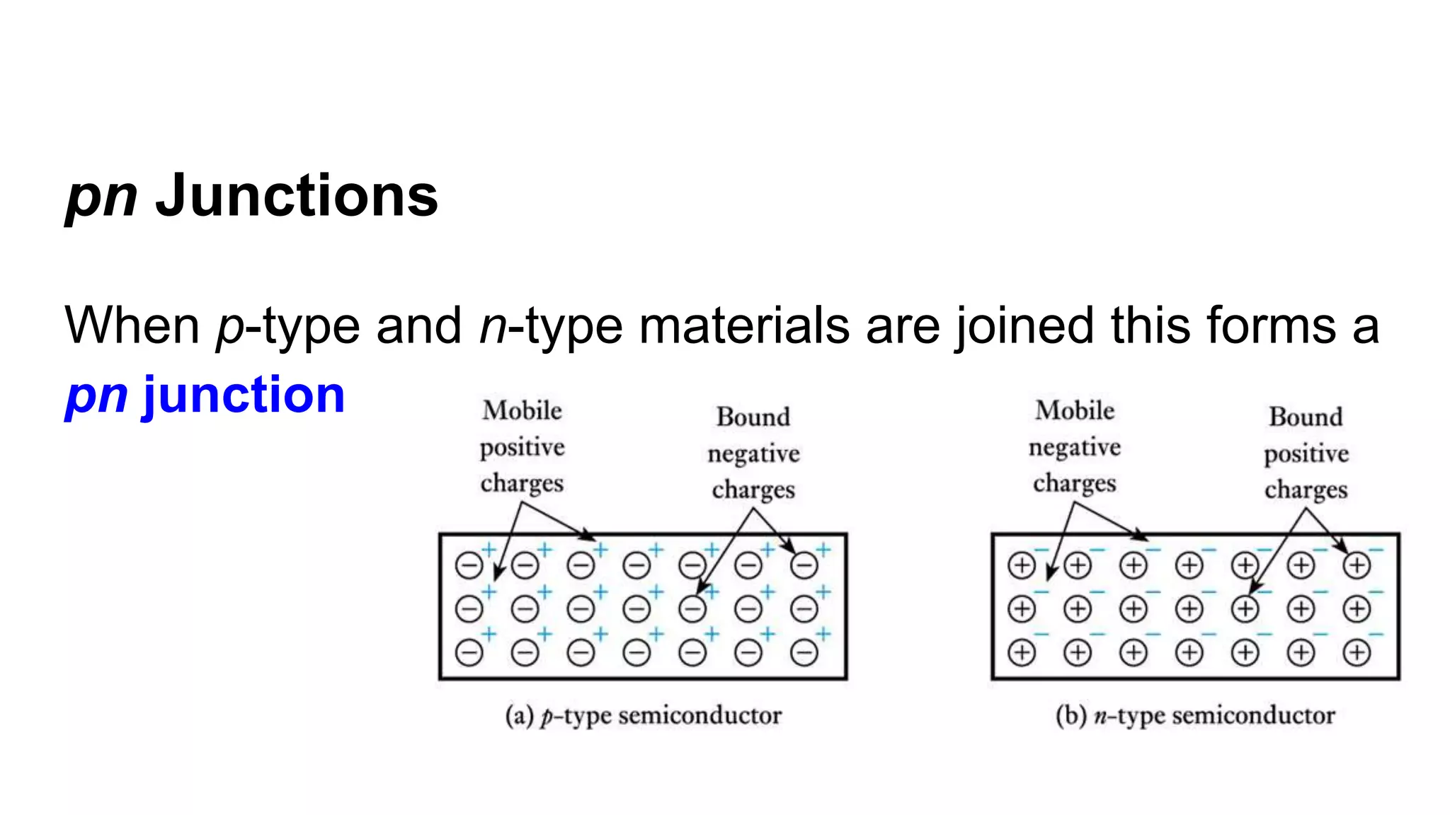
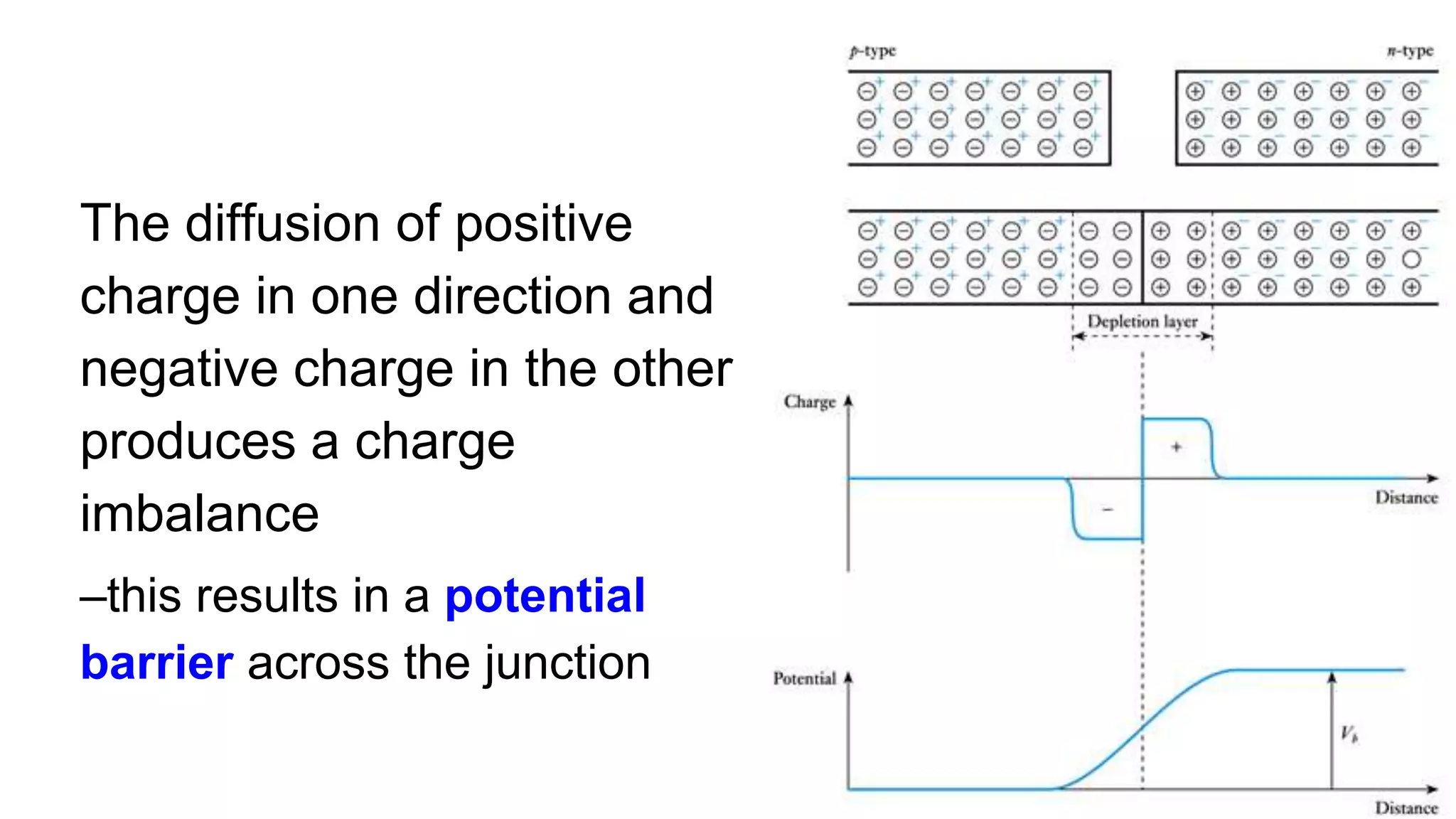
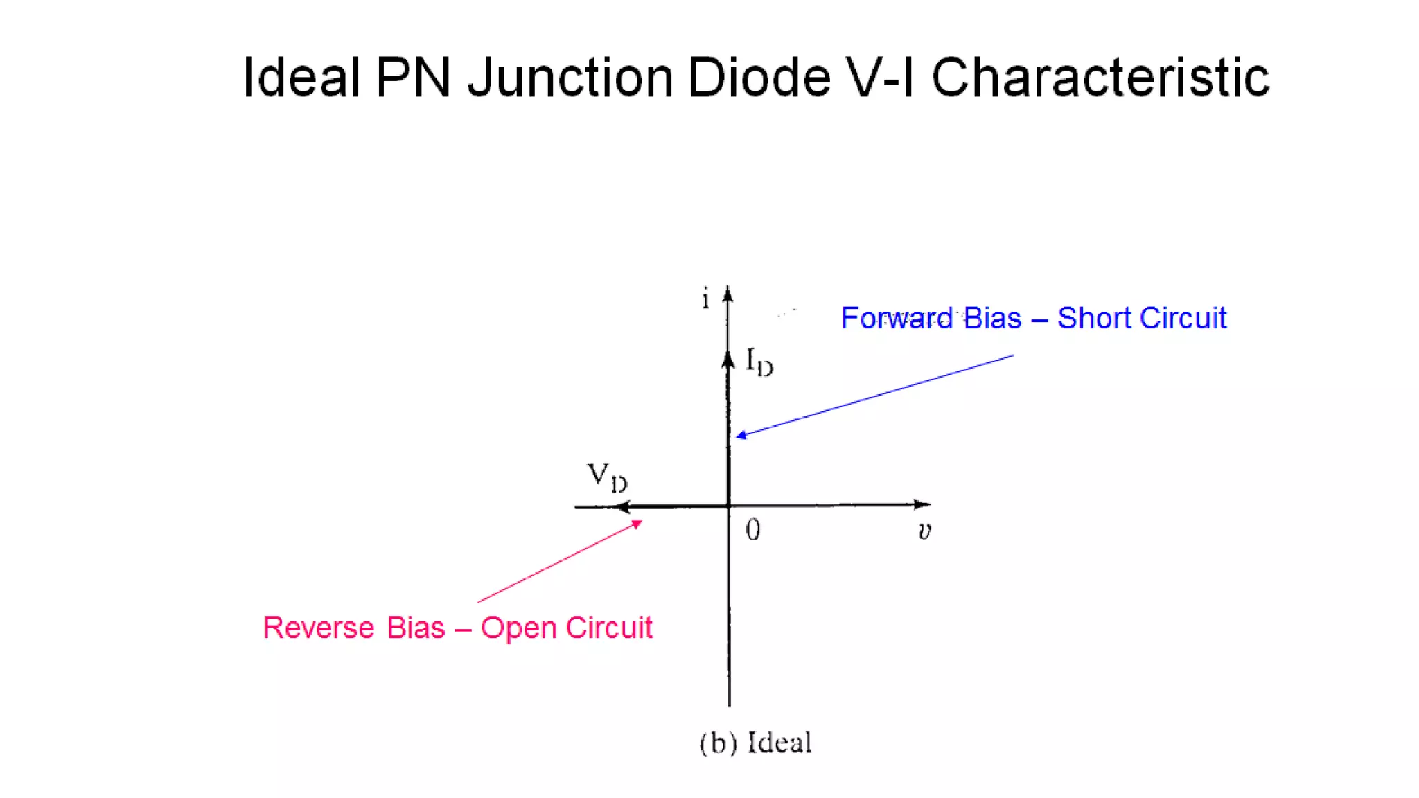
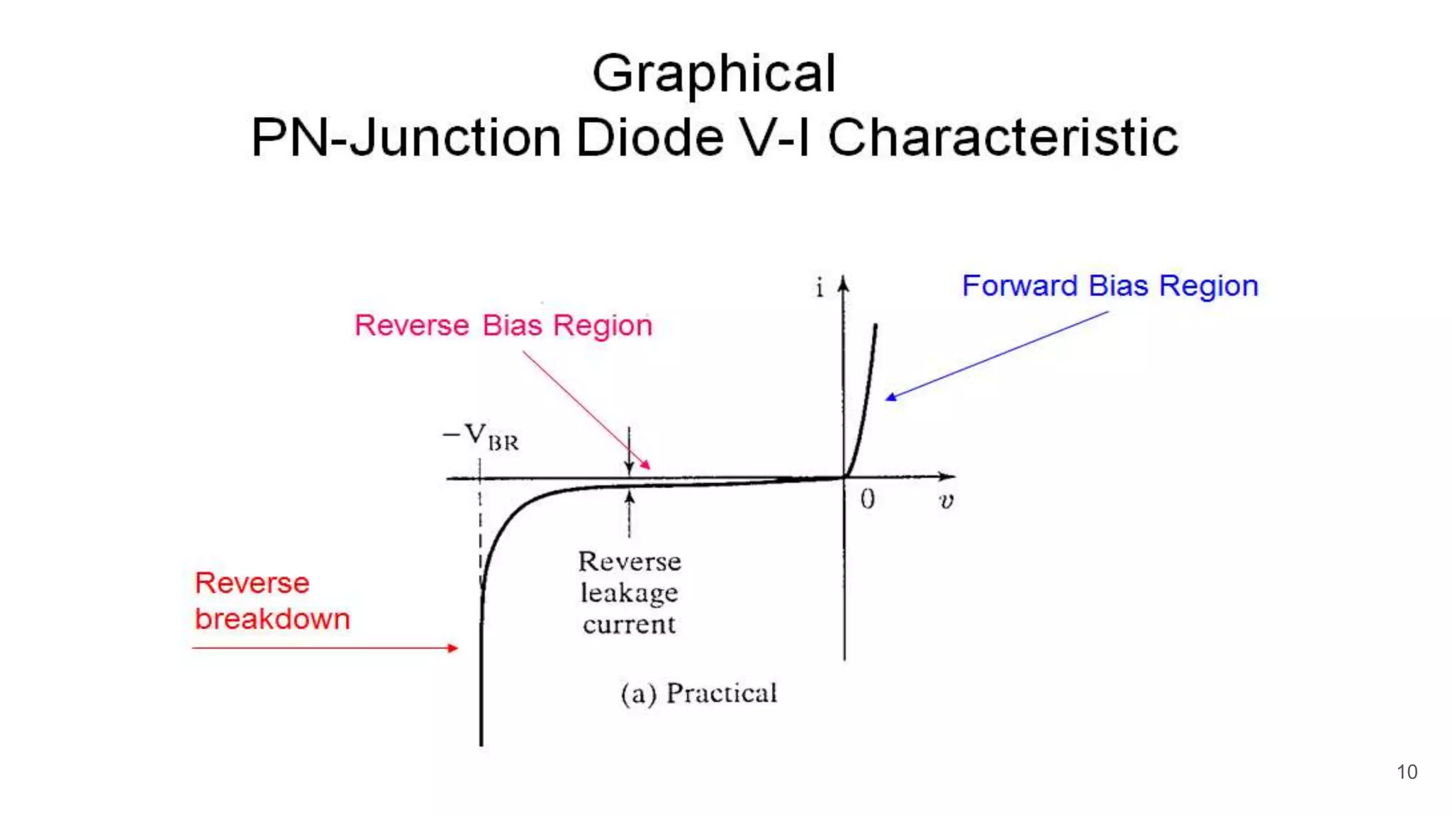
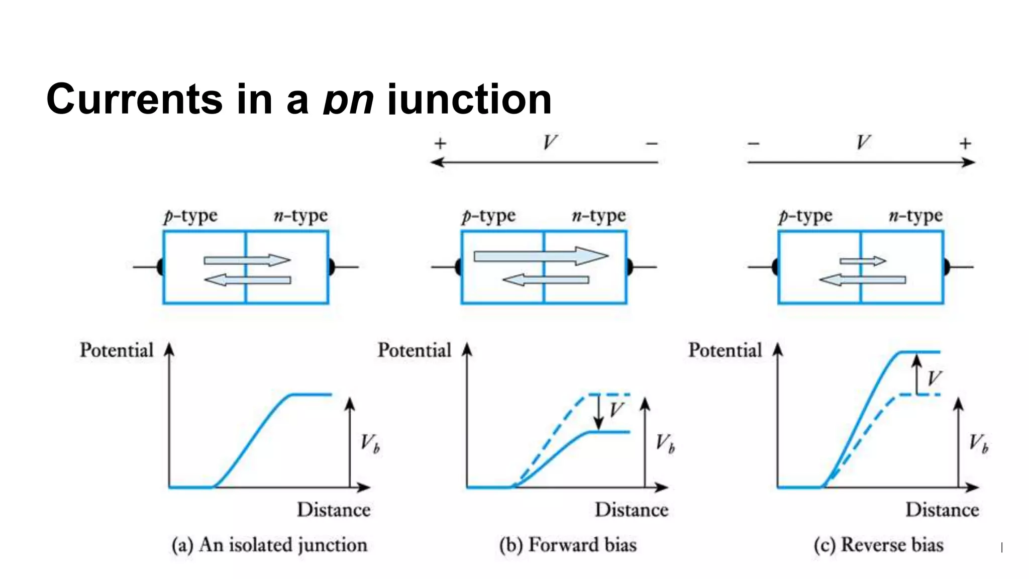
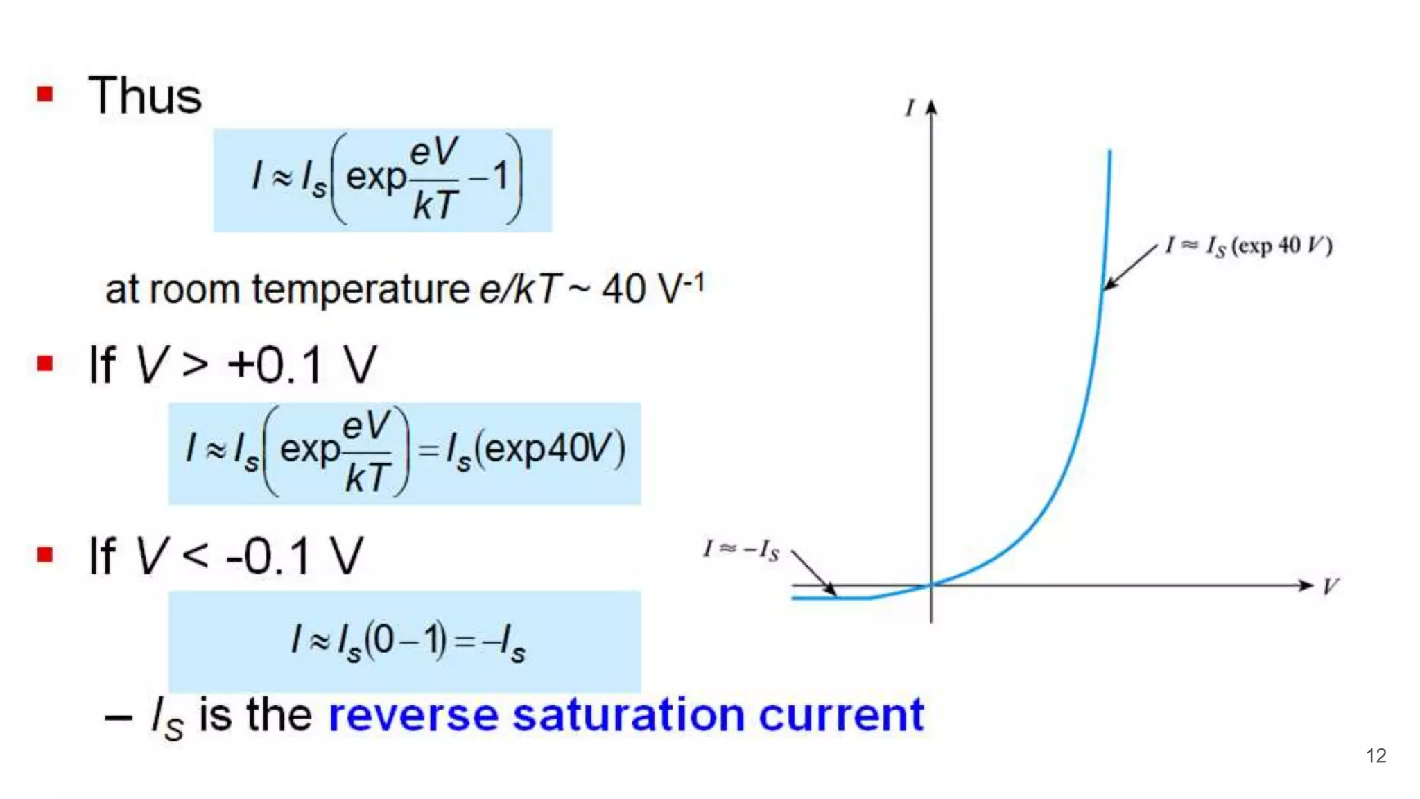
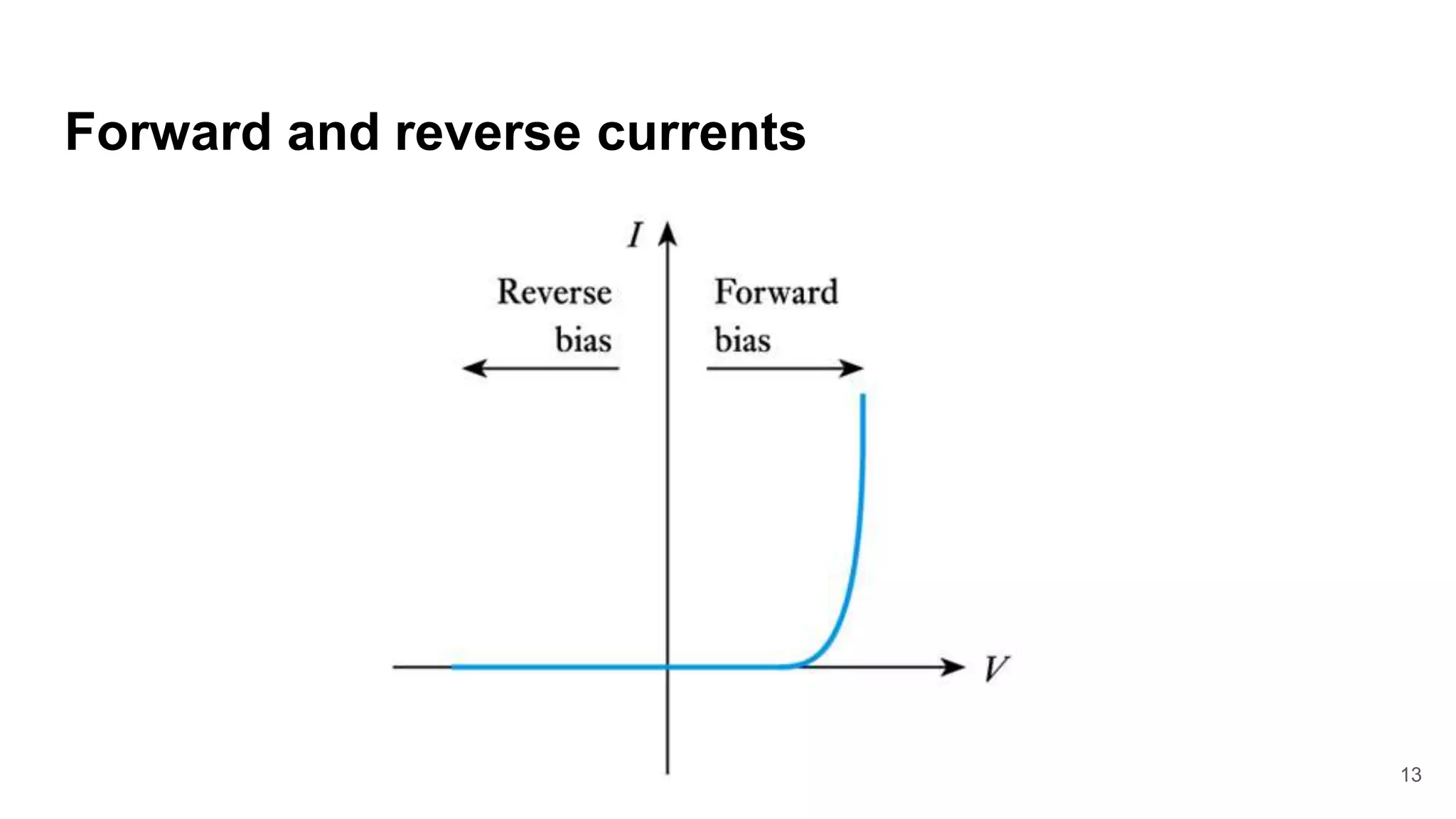
Diode Characteristics
D.A.Y.K Gunawardana
Department of computer science and informatics
diode
An ideal diode passing electricity in one direction but
not the other
3
pn Junctions
When p-type and n-type materials are joined this forms a
pn junction
–majority charge carriers on each side diffuse across the
junction where they combine with (and remove) charge
carriers of the opposite polarity
–hence around the junction there are few free charge carriers
and we have a depletion layer (also called a space-charge
layer)
The diffusion of positive
charge in one direction and
negative charge in the other
produces a charge
imbalance
–this results in a potential
barrier across the junction
Forward bias
–if the p-type side is made positive with respect to the
n-type side the height of the barrier is reduced
–more majority charge carriers have sufficient energy to
surmount it
–the diffusion current therefore increases while the drift
current remains the same
–there is thus a net current flow across the junction which
increases with the applied voltage
Reverse bias
–if the p-type side is made negative with respect to the
n-type side the height of the barrier is increased
–the number of majority charge carriers that have sufficient
energy to surmount it rapidly decreases
–the diffusion current therefore vanishes while the drift
current remains the same
–thus the only current is a small leakage current caused by
the (approximately constant) drift current
–the leakage current is usually negligible (a few nA)
10
Currents in a pn junction
11
12
Forward and reverse currents
13

Diode Characteristics

  • 1.
    Diode Characteristics D.A.Y.K Gunawardana Departmentof computer science and informatics
  • 2.
    diode An ideal diodepassing electricity in one direction but not the other
  • 3.
  • 4.
    pn Junctions When p-typeand n-type materials are joined this forms a pn junction
  • 5.
    –majority charge carrierson each side diffuse across the junction where they combine with (and remove) charge carriers of the opposite polarity –hence around the junction there are few free charge carriers and we have a depletion layer (also called a space-charge layer)
  • 6.
    The diffusion ofpositive charge in one direction and negative charge in the other produces a charge imbalance –this results in a potential barrier across the junction
  • 7.
    Forward bias –if thep-type side is made positive with respect to the n-type side the height of the barrier is reduced –more majority charge carriers have sufficient energy to surmount it –the diffusion current therefore increases while the drift current remains the same –there is thus a net current flow across the junction which increases with the applied voltage
  • 8.
    Reverse bias –if thep-type side is made negative with respect to the n-type side the height of the barrier is increased –the number of majority charge carriers that have sufficient energy to surmount it rapidly decreases –the diffusion current therefore vanishes while the drift current remains the same –thus the only current is a small leakage current caused by the (approximately constant) drift current –the leakage current is usually negligible (a few nA)
  • 10.
  • 11.
    Currents in apn junction 11
  • 12.
  • 13.