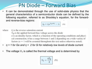
PN Diode – Forward Bias
• Forward-Bias Condition (VD + 0 V ) : A forward-bias or “on” condition is established
by applying the positive potential to the p -type material and the negative potential to
the n -type material as shown in Figure.
• The application of a forward-bias potential VD will “pressure” electrons in the n -type
material and holes in the p -type material to recombine with the ions near the
boundary and reduce the width of the depletion region .
• The resulting minority-carrier flow of electrons from the p -type material to the n -
type material (and of holes from the n –type material to the p -type material) has not
changed in magnitude (since the conduction level is controlled primarily by the
limited number of impurities in the material), but the reduction in the width of the
depletion region has resulted in a heavy majority flow across the junction
• As the applied bias increases in magnitude, the depletion region will continue to
decrease in width until a flood of electrons can pass through the junction, resulting in
an exponential rise in current as shown in the forward-bias region of the
characteristics of Figure and is measured in milliamperes.
PN Diode – Forward Bias
• The forward current increases very little until the forward voltage across
the PN junction reaches approximately 0.7 V at the knee of the curve.
• After this point, the forward voltage remains nearly constant at
approximately 0.7 V, but IF increases rapidly.
• Even if there is a slight increase in VF above 0.7 V , the current
increases due mainly to the voltage drop across the dynamic resistance.
• The IF scale is typically in mA, as indicated. Three points A, B, and C are
shown on the curve in Figure.
• Point A corresponds to a zero-bias condition.
• Point B corresponds where the forward voltage is less than the barrier
potential of 0.7 V.
• Point C corresponds where the forward voltage approximately equals
the barrier potential.
• As the external bias voltage and forward current continue to increase
above the knee, the forward voltage will increase slightly above 0.7 V
PN Diode – Forward Bias
• It can be demonstrated through the use of solid-state physics that the
general characteristics of a semiconductor diode can be defined by the
following equation, referred to as Shockley’s equation, for the forward-
and reverse-bias regions:
• η = 1 for Ge and η = 2 for Si for relatively low levels of diode current
• The voltage VT is called the thermal voltage and is determined by
VI Characteristics
• The equation is expanded as
• For positive values of VD the first term of the above equation will grow
very quickly and totally overpower the effect of the second term.
• The result is the following equation, which only has positive values and
takes on the exponential format ex appearing in Fig.
• The exponential curve of Figure increases very rapidly with increasing
values of x
VI Characteristics
Reverse-Bias Condition (VD < 0 V)
PN Diode : Reverse Bias
 The external potential of VD volts is applied across the p – n junction such
that the positive terminal is connected to the n -type material and the
negative terminal is connected to the p -type material as shown in Figure.
 The number of uncovered positive ions in the depletion region of the n -
type material will increase due to the large number of free electrons drawn
to the positive potential of the applied voltage.
 The number of uncovered negative ions will increase in the p -type
material. The net effect, therefore, is a widening of the depletion region.
 This widening of the depletion region will establish a barrier for the
majority carriers to overcome, effectively reducing the majority carrier flow
to zero
 The number of minority carriers, however, entering the depletion region
will not change, resulting in minority-carrier flow vectors of the same
magnitude indicated in Figure with no applied voltage.
• When a reverse-bias voltage is applied across a diode, there is only an
extremely small reverse current (IR) through the PN junction. With zero V
across the diode, there is no reverse current.
• As the reverse-bias voltage increased gradually, there is a very small
reverse current and the voltage across the diode increases.
• When the applied bias voltage is increased to a value where the reverse
voltage across the diode (VR) reaches the breakdown value (VBR), the
reverse current begins to increase rapidly
PN Diode : Reverse Bias
 The current that exists under reverse-bias conditions is called the
reverse saturation current and is represented by IS .
 The reverse saturation current is seldom more than a few
microamperes and typically in nA, except for high-power devices.
 The term saturation comes from the fact that it reaches its
maximum level quickly and does not change significantly with
increases in the reverse-bias potential, as shown on the diode
characteristics.
 For negative values of VD the exponential term drops very quickly
below the level of I , and the resulting equation for ID is simply
 ID ~ - IS ( VD negative).
 As VD = 0,
PN Diode : Reverse Bias
 The actual reverse saturation current of a commercially available diode will
normally be measurably larger than that appearing as the reverse saturation
current in Shockley’s equation.
This increase in level is due to a wide range of factors that include
– leakage currents
– generation of carriers in the depletion region
– higher doping levels that result in increased levels of reverse current
– sensitivity to the intrinsic level of carriers in the component materials by a
squared factor—double the intrinsic level, and the contribution to the reverse current
could increase by a factor of four.
– a direct relationship with the junction area—double the area of the junction,
and the contribution to the reverse current could double. High-power devices that
have larger junction areas typically have much higher levels of reverse current.
– temperature sensitivity—for every 10°C increase in temperature, the level of
reverse saturation current will double.
PN Diode : Reverse Bias
PN Junction Diode: VI Characteristics
 Temperature Effects For a forward-biased diode, as temperature is
increased, the forward current increases for a given value of forward
voltage.
 Also, for a given value of forward current, the forward voltage decreases.
This is shown with the V-I characteristic curves in Figure.
 The blue curve is at room temperature 25°C and the red curve is at an
elevated temperature (25°C + ΔT ) .
 The barrier potential decreases by 2 mV for each degree increase in
temperature.
VI Characteristics : Effect on Temperature

PN Diode VI Characteristics.pptx

  • 2.
    PN Diode –Forward Bias
  • 3.
    PN Diode –Forward Bias • Forward-Bias Condition (VD + 0 V ) : A forward-bias or “on” condition is established by applying the positive potential to the p -type material and the negative potential to the n -type material as shown in Figure. • The application of a forward-bias potential VD will “pressure” electrons in the n -type material and holes in the p -type material to recombine with the ions near the boundary and reduce the width of the depletion region . • The resulting minority-carrier flow of electrons from the p -type material to the n - type material (and of holes from the n –type material to the p -type material) has not changed in magnitude (since the conduction level is controlled primarily by the limited number of impurities in the material), but the reduction in the width of the depletion region has resulted in a heavy majority flow across the junction • As the applied bias increases in magnitude, the depletion region will continue to decrease in width until a flood of electrons can pass through the junction, resulting in an exponential rise in current as shown in the forward-bias region of the characteristics of Figure and is measured in milliamperes.
  • 4.
    PN Diode –Forward Bias
  • 5.
    PN Diode –Forward Bias • The forward current increases very little until the forward voltage across the PN junction reaches approximately 0.7 V at the knee of the curve. • After this point, the forward voltage remains nearly constant at approximately 0.7 V, but IF increases rapidly. • Even if there is a slight increase in VF above 0.7 V , the current increases due mainly to the voltage drop across the dynamic resistance. • The IF scale is typically in mA, as indicated. Three points A, B, and C are shown on the curve in Figure. • Point A corresponds to a zero-bias condition. • Point B corresponds where the forward voltage is less than the barrier potential of 0.7 V. • Point C corresponds where the forward voltage approximately equals the barrier potential. • As the external bias voltage and forward current continue to increase above the knee, the forward voltage will increase slightly above 0.7 V
  • 6.
    PN Diode –Forward Bias • It can be demonstrated through the use of solid-state physics that the general characteristics of a semiconductor diode can be defined by the following equation, referred to as Shockley’s equation, for the forward- and reverse-bias regions: • η = 1 for Ge and η = 2 for Si for relatively low levels of diode current • The voltage VT is called the thermal voltage and is determined by
  • 8.
    VI Characteristics • Theequation is expanded as • For positive values of VD the first term of the above equation will grow very quickly and totally overpower the effect of the second term. • The result is the following equation, which only has positive values and takes on the exponential format ex appearing in Fig. • The exponential curve of Figure increases very rapidly with increasing values of x
  • 9.
  • 10.
  • 11.
    PN Diode :Reverse Bias  The external potential of VD volts is applied across the p – n junction such that the positive terminal is connected to the n -type material and the negative terminal is connected to the p -type material as shown in Figure.  The number of uncovered positive ions in the depletion region of the n - type material will increase due to the large number of free electrons drawn to the positive potential of the applied voltage.  The number of uncovered negative ions will increase in the p -type material. The net effect, therefore, is a widening of the depletion region.  This widening of the depletion region will establish a barrier for the majority carriers to overcome, effectively reducing the majority carrier flow to zero  The number of minority carriers, however, entering the depletion region will not change, resulting in minority-carrier flow vectors of the same magnitude indicated in Figure with no applied voltage.
  • 12.
    • When areverse-bias voltage is applied across a diode, there is only an extremely small reverse current (IR) through the PN junction. With zero V across the diode, there is no reverse current. • As the reverse-bias voltage increased gradually, there is a very small reverse current and the voltage across the diode increases. • When the applied bias voltage is increased to a value where the reverse voltage across the diode (VR) reaches the breakdown value (VBR), the reverse current begins to increase rapidly PN Diode : Reverse Bias
  • 13.
     The currentthat exists under reverse-bias conditions is called the reverse saturation current and is represented by IS .  The reverse saturation current is seldom more than a few microamperes and typically in nA, except for high-power devices.  The term saturation comes from the fact that it reaches its maximum level quickly and does not change significantly with increases in the reverse-bias potential, as shown on the diode characteristics.  For negative values of VD the exponential term drops very quickly below the level of I , and the resulting equation for ID is simply  ID ~ - IS ( VD negative).  As VD = 0, PN Diode : Reverse Bias
  • 14.
     The actualreverse saturation current of a commercially available diode will normally be measurably larger than that appearing as the reverse saturation current in Shockley’s equation. This increase in level is due to a wide range of factors that include – leakage currents – generation of carriers in the depletion region – higher doping levels that result in increased levels of reverse current – sensitivity to the intrinsic level of carriers in the component materials by a squared factor—double the intrinsic level, and the contribution to the reverse current could increase by a factor of four. – a direct relationship with the junction area—double the area of the junction, and the contribution to the reverse current could double. High-power devices that have larger junction areas typically have much higher levels of reverse current. – temperature sensitivity—for every 10°C increase in temperature, the level of reverse saturation current will double. PN Diode : Reverse Bias
  • 15.
    PN Junction Diode:VI Characteristics
  • 16.
    PN Junction Diode:VI Characteristics
  • 17.
    PN Junction Diode:VI Characteristics
  • 18.
     Temperature EffectsFor a forward-biased diode, as temperature is increased, the forward current increases for a given value of forward voltage.  Also, for a given value of forward current, the forward voltage decreases. This is shown with the V-I characteristic curves in Figure.  The blue curve is at room temperature 25°C and the red curve is at an elevated temperature (25°C + ΔT ) .  The barrier potential decreases by 2 mV for each degree increase in temperature. VI Characteristics : Effect on Temperature