Download to read offline
![International Journal of Latest Technology in Engineering, Management & Applied Science (IJLTEMAS)
Volume IX, Is
www.ijltemas.in
Design of Multiplexers, Decoder and a Full
Subtractor using Reversible Gates
Soham Bhattacharya
1,2,3
Electronics and Communication Engineering Department, Heritage Institut
Abstract- This paper shows an effective design of
circuits such as 2:1, 4:1 multiplexers, 2:4 decoder and a full
subtractor using reversible gates. This paper also evaluates
number of reversible gates used and garbage output
implementing each combinational circuit.
Keywords - Reversible Logic Gates, Multiplexer
Subtractor Garbage output
I. INTRODUCTION
n the early 1960, R. Landauer proved that irreversible
computation results in KTln2 joules of energy dissipation
due to the each bit of information loss where K = Boltzmann’s
constant, T = Temperature at which computation is performed
[1]. Later in 1973, C.H. Bennett showed that KTln2 joules of
energy dissipation can be eliminated, if the computation is
performed in a reversible manner [2].
A multiplexer or MUX is a device that selects between
different analog or digital input signals and forwards it to a
single output signal. A MUX of 2n
inputs has n select lines,
which are used to select which input line is to be sent to the
output. A decoder is a combinational circuit that converts
binary information from n input lines to a maximum of 2
unique output lines [3]. A full Subtractor is a combinational
circuit that performs subtraction of two bits, one is minuend
and other is subtrahend. The full subtractor circuit has three
inputs and two outputs. The three inputs A, B and Bin, denote
the minuend, subtrahend and previous borrow respectively.
The two outputs D and Bout represent the difference and
output borrows respectively.
II. REVERSIBLE LOGIC
‘Reversible Computation’ is defined as a model of
computation where computational process at some extent, is
reversible. It means that it can reserve the data as long as it
requires and when needed [4]. Reversible gate is basically
n X n logic gate, where, if ‘n’ inputs are given, we will get ‘n’
outputs. Properties of reversible logic are like it can recover
the state of inputs from the outputs, it follows bijective
mapping i.e. when ‘n’ number of inputs are taken, and one can
get ‘n’ number of outputs from the gates. The circuit obtained
will be acyclic, i.e. feedback will be there but Fan
be more than one. Parameters to determine the complexity and
performance of circuits[5,6] are the number of reversible
gates, garbage output which is the number of unused outputs
I
International Journal of Latest Technology in Engineering, Management & Applied Science (IJLTEMAS)
Volume IX, Issue II, February 2020 | ISSN 2278-2540
esign of Multiplexers, Decoder and a Full
Subtractor using Reversible Gates
Soham Bhattacharya1
, Sourav Goswami2
, Anindya Sen3
Electronics and Communication Engineering Department, Heritage Institute of Technology, Kolkata, India
design of combinational
2:1, 4:1 multiplexers, 2:4 decoder and a full
This paper also evaluates
garbage outputs in
, Multiplexer, Decoder, Full
n the early 1960, R. Landauer proved that irreversible
in KTln2 joules of energy dissipation
due to the each bit of information loss where K = Boltzmann’s
constant, T = Temperature at which computation is performed
[1]. Later in 1973, C.H. Bennett showed that KTln2 joules of
ed, if the computation is
A multiplexer or MUX is a device that selects between
different analog or digital input signals and forwards it to a
inputs has n select lines,
d to select which input line is to be sent to the
A decoder is a combinational circuit that converts
binary information from n input lines to a maximum of 2n
A full Subtractor is a combinational
ction of two bits, one is minuend
and other is subtrahend. The full subtractor circuit has three
B and Bin, denote
the minuend, subtrahend and previous borrow respectively.
the difference and
‘Reversible Computation’ is defined as a model of
computation where computational process at some extent, is
reversible. It means that it can reserve the data as long as it
hen needed [4]. Reversible gate is basically an
n X n logic gate, where, if ‘n’ inputs are given, we will get ‘n’
Properties of reversible logic are like it can recover
the state of inputs from the outputs, it follows bijective
n’ number of inputs are taken, and one can
get ‘n’ number of outputs from the gates. The circuit obtained
will be acyclic, i.e. feedback will be there but Fan-out will not
Parameters to determine the complexity and
[5,6] are the number of reversible
the number of unused outputs
used in the reversible gates, and quantum cost which is the
cost of the circuit with respect to the cost of a primitive
gate.In the past few decades, the Reversible logic has emerged
as one of the promising research areas find its applications in
various emerging technologies such as Bioinformatics,
Cryptography, Optical computing, Nanotechnology, DNA
computing, and Quantum computing etc
III. REVERSIBLE GATES USED
There are several number of reversible gates used to
implement various complex circuits, but
have used 3X3 NFT GATE to implement multiplexer
2:1 and 4:1), 3X3 TOFFOLI GATE to implement 2:4
and three reversible gates (4X4
FEYNMANN GATE, 3X3 FREDKIN GATE) to implement a
full subtractor using two half subtractor
1. NFT Gate:
It is a 3X3 gate with inputs A, B and C and outputs X, Y and
Z, where X = A XOR B, Y = B’C XOR AC,
AC’.
Fig.1 denotes the basic logic diagram of NFT
2. TOFFOLI Gate:
It is a 3X3 reversible gate with inputs A, B and C and outputs
X, Y and Z, where X = A,
Y = B, Z = (A.B) XOR C [8].
Fig. 2 denotes the basic logic diagram of TOFFOLI
International Journal of Latest Technology in Engineering, Management & Applied Science (IJLTEMAS)
Page 106
esign of Multiplexers, Decoder and a Full
Subtractor using Reversible Gates
e of Technology, Kolkata, India
and quantum cost which is the
cost of the circuit with respect to the cost of a primitive
n the past few decades, the Reversible logic has emerged
as one of the promising research areas find its applications in
various emerging technologies such as Bioinformatics,
Cryptography, Optical computing, Nanotechnology, DNA
ting etc [7].
REVERSIBLE GATES USED
There are several number of reversible gates used to
implement various complex circuits, but in this paper, we
NFT GATE to implement multiplexers (both
TOFFOLI GATE to implement 2:4 Decoder
4X4 HNG GATE, 2X2
FREDKIN GATE) to implement a
full subtractor using two half subtractors.
It is a 3X3 gate with inputs A, B and C and outputs X, Y and
Z, where X = A XOR B, Y = B’C XOR AC, Z = BC XOR
logic diagram of NFT Gate
It is a 3X3 reversible gate with inputs A, B and C and outputs
logic diagram of TOFFOLI Gate](https://image.slidesharecdn.com/106-110-200404062245/85/Design-of-Multiplexers-Decoder-and-a-Full-Subtractor-using-Reversible-Gates-1-320.jpg)
![International Journal of Latest Technology in Engineering, Management & Applied Science (IJLTEMAS)
Volume IX, Is
www.ijltemas.in
Design of Multiplexers, Decoder and a Full
Subtractor using Reversible Gates
Soham Bhattacharya
1,2,3
Electronics and Communication Engineering Department, Heritage Institut
Abstract- This paper shows an effective design of
circuits such as 2:1, 4:1 multiplexers, 2:4 decoder and a full
subtractor using reversible gates. This paper also evaluates
number of reversible gates used and garbage output
implementing each combinational circuit.
Keywords - Reversible Logic Gates, Multiplexer
Subtractor Garbage output
I. INTRODUCTION
n the early 1960, R. Landauer proved that irreversible
computation results in KTln2 joules of energy dissipation
due to the each bit of information loss where K = Boltzmann’s
constant, T = Temperature at which computation is performed
[1]. Later in 1973, C.H. Bennett showed that KTln2 joules of
energy dissipation can be eliminated, if the computation is
performed in a reversible manner [2].
A multiplexer or MUX is a device that selects between
different analog or digital input signals and forwards it to a
single output signal. A MUX of 2n
inputs has n select lines,
which are used to select which input line is to be sent to the
output. A decoder is a combinational circuit that converts
binary information from n input lines to a maximum of 2
unique output lines [3]. A full Subtractor is a combinational
circuit that performs subtraction of two bits, one is minuend
and other is subtrahend. The full subtractor circuit has three
inputs and two outputs. The three inputs A, B and Bin, denote
the minuend, subtrahend and previous borrow respectively.
The two outputs D and Bout represent the difference and
output borrows respectively.
II. REVERSIBLE LOGIC
‘Reversible Computation’ is defined as a model of
computation where computational process at some extent, is
reversible. It means that it can reserve the data as long as it
requires and when needed [4]. Reversible gate is basically
n X n logic gate, where, if ‘n’ inputs are given, we will get ‘n’
outputs. Properties of reversible logic are like it can recover
the state of inputs from the outputs, it follows bijective
mapping i.e. when ‘n’ number of inputs are taken, and one can
get ‘n’ number of outputs from the gates. The circuit obtained
will be acyclic, i.e. feedback will be there but Fan
be more than one. Parameters to determine the complexity and
performance of circuits[5,6] are the number of reversible
gates, garbage output which is the number of unused outputs
I
International Journal of Latest Technology in Engineering, Management & Applied Science (IJLTEMAS)
Volume IX, Issue II, February 2020 | ISSN 2278-2540
esign of Multiplexers, Decoder and a Full
Subtractor using Reversible Gates
Soham Bhattacharya1
, Sourav Goswami2
, Anindya Sen3
Electronics and Communication Engineering Department, Heritage Institute of Technology, Kolkata, India
design of combinational
2:1, 4:1 multiplexers, 2:4 decoder and a full
This paper also evaluates
garbage outputs in
, Multiplexer, Decoder, Full
n the early 1960, R. Landauer proved that irreversible
in KTln2 joules of energy dissipation
due to the each bit of information loss where K = Boltzmann’s
constant, T = Temperature at which computation is performed
[1]. Later in 1973, C.H. Bennett showed that KTln2 joules of
ed, if the computation is
A multiplexer or MUX is a device that selects between
different analog or digital input signals and forwards it to a
inputs has n select lines,
d to select which input line is to be sent to the
A decoder is a combinational circuit that converts
binary information from n input lines to a maximum of 2n
A full Subtractor is a combinational
ction of two bits, one is minuend
and other is subtrahend. The full subtractor circuit has three
B and Bin, denote
the minuend, subtrahend and previous borrow respectively.
the difference and
‘Reversible Computation’ is defined as a model of
computation where computational process at some extent, is
reversible. It means that it can reserve the data as long as it
hen needed [4]. Reversible gate is basically an
n X n logic gate, where, if ‘n’ inputs are given, we will get ‘n’
Properties of reversible logic are like it can recover
the state of inputs from the outputs, it follows bijective
n’ number of inputs are taken, and one can
get ‘n’ number of outputs from the gates. The circuit obtained
will be acyclic, i.e. feedback will be there but Fan-out will not
Parameters to determine the complexity and
[5,6] are the number of reversible
the number of unused outputs
used in the reversible gates, and quantum cost which is the
cost of the circuit with respect to the cost of a primitive
gate.In the past few decades, the Reversible logic has emerged
as one of the promising research areas find its applications in
various emerging technologies such as Bioinformatics,
Cryptography, Optical computing, Nanotechnology, DNA
computing, and Quantum computing etc
III. REVERSIBLE GATES USED
There are several number of reversible gates used to
implement various complex circuits, but
have used 3X3 NFT GATE to implement multiplexer
2:1 and 4:1), 3X3 TOFFOLI GATE to implement 2:4
and three reversible gates (4X4
FEYNMANN GATE, 3X3 FREDKIN GATE) to implement a
full subtractor using two half subtractor
1. NFT Gate:
It is a 3X3 gate with inputs A, B and C and outputs X, Y and
Z, where X = A XOR B, Y = B’C XOR AC,
AC’.
Fig.1 denotes the basic logic diagram of NFT
2. TOFFOLI Gate:
It is a 3X3 reversible gate with inputs A, B and C and outputs
X, Y and Z, where X = A,
Y = B, Z = (A.B) XOR C [8].
Fig. 2 denotes the basic logic diagram of TOFFOLI
International Journal of Latest Technology in Engineering, Management & Applied Science (IJLTEMAS)
Page 106
esign of Multiplexers, Decoder and a Full
Subtractor using Reversible Gates
e of Technology, Kolkata, India
and quantum cost which is the
cost of the circuit with respect to the cost of a primitive
n the past few decades, the Reversible logic has emerged
as one of the promising research areas find its applications in
various emerging technologies such as Bioinformatics,
Cryptography, Optical computing, Nanotechnology, DNA
ting etc [7].
REVERSIBLE GATES USED
There are several number of reversible gates used to
implement various complex circuits, but in this paper, we
NFT GATE to implement multiplexers (both
TOFFOLI GATE to implement 2:4 Decoder
4X4 HNG GATE, 2X2
FREDKIN GATE) to implement a
full subtractor using two half subtractors.
It is a 3X3 gate with inputs A, B and C and outputs X, Y and
Z, where X = A XOR B, Y = B’C XOR AC, Z = BC XOR
logic diagram of NFT Gate
It is a 3X3 reversible gate with inputs A, B and C and outputs
logic diagram of TOFFOLI Gate](https://image.slidesharecdn.com/106-110-200404062245/75/Design-of-Multiplexers-Decoder-and-a-Full-Subtractor-using-Reversible-Gates-1-2048.jpg)
![International Journal of Latest Technology in Engineering, Management & Applied Science (IJLTEMAS)
Volume IX, Is
www.ijltemas.in
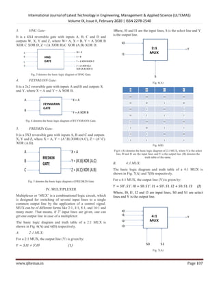
Fig. 10 shows the implementation of 2:4 Decoder using four
Gates and two 1X1 NOT gates, where A, B are the input lines and I0, I1, I
and I3 are the output lines.
VI. FULL SUBTRACTOR
A subtractor can be designed like an adder using same
approach. A full subtractor is a combinational circuit, used to
perform subtraction of three inputs, the minuend, the
subtrahend and borrow in. Two output lines are generated
which are difference and borrow out. A reversible half
subtractor is designed using two TSG gates
subtractor can be designed using two half subtractors.
Difference output and borrow out output can be given as:
𝐷𝑖𝑓𝑓𝑒𝑟𝑒𝑛𝑐𝑒 = 𝐴 𝑋𝑂𝑅 𝐵 𝑋𝑂𝑅 𝐵𝑖𝑛
𝐵𝑜𝑟𝑟𝑜𝑤 𝑜𝑢𝑡 = (𝐴 𝑋𝑂𝑅 𝐵) . 𝐵𝑖𝑛 𝑋𝑂𝑅 (𝐴 . 𝐵)
Where, A, B and Bin are the inputs and Difference and
Borrow out are the outputs.
The block diagram and truth table of a Full Subtractor is
shown in Fig. 11(A) and (B) respectively.
Fig. 11(A)
International Journal of Latest Technology in Engineering, Management & Applied Science (IJLTEMAS)
Volume IX, Issue II, February 2020 | ISSN 2278-2540
the implementation of 2:4 Decoder using four 3X3 TOFFOLI
, B are the input lines and I0, I1, I2
A subtractor can be designed like an adder using same
subtractor is a combinational circuit, used to
, the minuend, the
subtrahend and borrow in. Two output lines are generated
A reversible half
subtractor is designed using two TSG gates in [4]. A full
subtractor can be designed using two half subtractors.
Difference output and borrow out output can be given as:
(7)
) (8)
Where, A, B and Bin are the inputs and Difference and
The block diagram and truth table of a Full Subtractor is
A B Bin
0 0 0
0 0 1
0 1 0
0 1 1
1 0 0
1 0 1
1 1 0
1 1 1
Fig. 11(B)
Fig.11: (A) denotes the basic block diagram of Full Subtractor, where A, B,
and Bin are the input lines, and Diff denotes difference output line, and Bout
denotes the borrow out output line. (B) denotes the truth table of the same
B. Full Subtractor Using Reversible Gates:
A full subtractor circuit can be implemented using three
reversible gates, such as 4X4 HNG gate,
gate and 3X3 FREDKIN gate in Fig.12.
Fig. 12 shows the implementation of Full Subtractor using reversible gates,
where A, B and Bin are the input lines and Diff denotes the Difference output
line and Borrow denotes the borrow output
VII. PERFORMANCE ANALYSIS
METHODS
GARBAGE
OUTPUTS
2:1 MUX 2
4:1 MUX 8
2:4 DECODER 8
FULL SUBTRACTOR 4
Fig. 13 shows the performance details of number of
the above implementations.
International Journal of Latest Technology in Engineering, Management & Applied Science (IJLTEMAS)
Page 109
Diff Bout
0 0
1 1
1 1
0 1
1 0
0 0
0 0
1 1
Fig. 11(B)
Fig.11: (A) denotes the basic block diagram of Full Subtractor, where A, B,
and Diff denotes difference output line, and Bout
denotes the borrow out output line. (B) denotes the truth table of the same.
Full Subtractor Using Reversible Gates:
A full subtractor circuit can be implemented using three
NG gate, 2X2 FEYNMANN
FREDKIN gate in Fig.12.
the implementation of Full Subtractor using reversible gates,
Diff denotes the Difference output
line and Borrow denotes the borrow output line.
VII. PERFORMANCE ANALYSIS
GARBAGE
OUTPUTS
NO. OF
REVERSIBLE
GATES
1
3
6
3
Fig. 13 shows the performance details of number of gates, garbage outputs of
the above implementations.](https://image.slidesharecdn.com/106-110-200404062245/85/Design-of-Multiplexers-Decoder-and-a-Full-Subtractor-using-Reversible-Gates-4-320.jpg)
![International Journal of Latest Technology in Engineering, Management & Applied Science (IJLTEMAS)
Volume IX, Issue II, February 2020 | ISSN 2278-2540
www.ijltemas.in Page 110
The table of Fig. 13 shows the performance of the
implemented device using reversible gates in terms of number
of gates and the garbage outputs.
VIII. CONCLUSION
In this paper, 2:1 and 4:1 multiplexers, 2:4 decoder and a full
subtractor has been implemented using reversible gates in an
efficient way. For the designing of 2:1 and 4:1 multiplexers,
numbers of gates used are 1 and 3. Garbage outputs are 2 and
8 respectively. For the designing of 2:4 decoder, the number
of gates used and garbage outputs are 6 and 8 respectively and
in case of a full subtractor, number of gates used are 3 and
garbage outputs are 4. So, one can implement these
combinational circuits using these reversible gates from the
details shown in the table.
REFERENCES
[1] R. Landauer in “Irreversibility and Heat Generation in the
Computing Process”. IBM J. Research and Development,5(3): pp.
183-191, 1961.
[2] Charles H. Bennett , in "Logical Reversibility of computation",
IBM Journal of Research and Development, vol. 17, no. 6, pp.
525-532, 1973.
[3] M.Morris Mano.: Digital Design. Prentice Hall Publisher (2001)
[4] Soham Bhattacharya, Anindya Sen "Power and Delay Analysis of
Logic Circuits Using Reversible Gates" International Journal of
Latest Technology in Engineering, Management & Applied
Science-IJLTEMAS vol.8 issue 12, December 2019, pp.54-63.
[5] M. Mohammadi and M. Eshghi, “On figures of merit in reversible
and quantum logic designs,” Quantum Information Processing,
vol. 8,no. 4, pp. 297–318, Aug. 2009.
[6] D. Maslov and G. W. Dueck, “Improved quantum cost for n-bit
toffoli gates” IEE Electronics Letters, vol. 39, no. 25, pp. 1790–
1791, Dec.2003.
[7] Design of a Multiplexer Using Reversible Logic Gowthami. P ,
R.V.S. Satyanarayana.
[8] Soham Bhattacharya, Sourav Goswami “Truth Table Analysis of
Logic Circuits using Reversible Gates” International Journal for
Research in Applied Science & Engineering Technology
(IJRASET) Volume 8 Issue II Feb 2020.](https://image.slidesharecdn.com/106-110-200404062245/85/Design-of-Multiplexers-Decoder-and-a-Full-Subtractor-using-Reversible-Gates-5-320.jpg)

The paper presents the design of 2:1, 4:1 multiplexers, a 2:4 decoder, and a full subtractor using reversible logic gates, emphasizing energy efficiency by minimizing garbage outputs. It discusses the reversible computation model and evaluates various reversible gates employed for these circuit designs. The findings highlight the complexity, performance metrics, and potential applications of reversible logic in emerging technologies.