Download to read offline

![International Research Journal of Engineering and Technology (IRJET) e-ISSN: 2395-0056
Volume: 04 Issue: 10 | Oct -2017 www.irjet.net p-ISSN: 2395-0072
© 2017, IRJET | Impact Factor value: 5.181 | ISO 9001:2008 Certified Journal | Page 368
3. DESIGN OF ENCRYPTION BY RRG GATE
The general idea of a cipher built from reversible gates was
presented Figure 5.
The basic element of the cipher is a cascade of 16 4-input
reversible gates. The same main key is used for data
encryption and decryption. The order of gatesinthecascade
for decryption is reversed in comparison with the cascade
for encryption that ensures that it transforms cipher-text
into plaintext.
Figure 5: The General idea of a cipher for encryption and
decryption
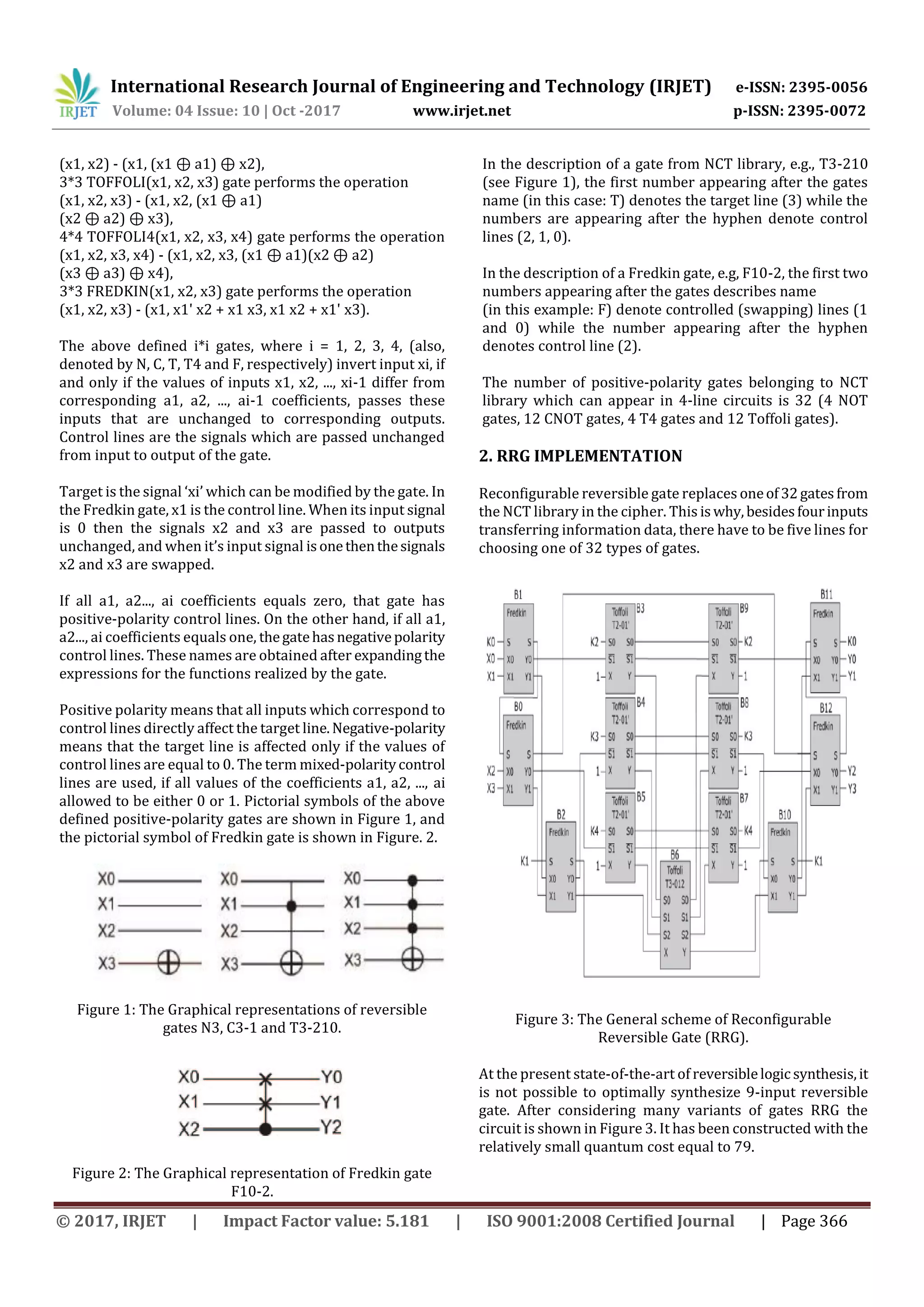
It has been proved that optimal circuits for any of the 16!
(Equal to over 2x10¹³) require at most 15 4-input gates.
Thus the circuit shown in Figure 6 enables the realization of
any 4-variable reversible function. The circuit has K which
denotes 80 inputs that are partitioned into groups with five
inputs in each of them.
A 5-line group K [(5*(i+1) – 1):5*i] is used to configure with
RRG gate. All inputs K are transferred to outputs so they can
be reused for controlling the next gate.
There are 4 data inputs X [3:0] and three lines with constant
inputs (equal to 1) and equivalent outputs.
A detailed description of the main key register, as well asthe
circuit modifying its contents, during encryption and
decryption, are presented in following figures.
Figure 6: The cascade of reversible gates implementing the
4-bit cipher.
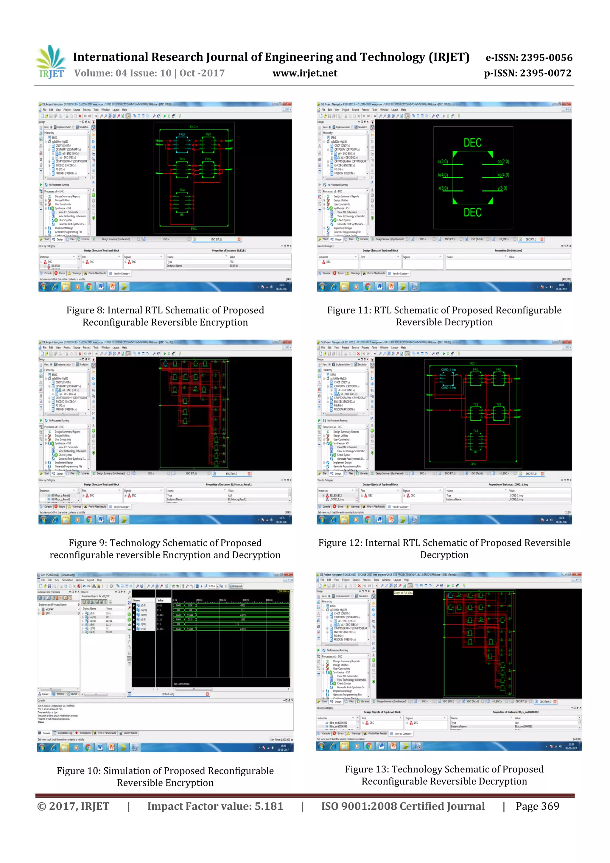
4. SYNTHESIS AND SIMULATION RESULTS
For encryption and decryption, a 5-bit key, two 4-bitciphers
and the main key, a register was used. In this section, first,
we will see the synthesis and simulation of the Encryption
and Decryption using a reconfigurable reversible gate.
Encryption and Decryption using reconfigurable reversible
gates are designed on Xilinx ISE 14.7 with Verilog HDL. The
RTL schematics and simulation results of the proposed
design are shown below.
Figure 7: RTL Schematic of Proposed Reconfigurable
Reversible Encryption](https://image.slidesharecdn.com/irjet-v4i1065-171124100356/75/An-Efficient-Design-for-Data-Encryption-and-Decryption-using-Reconfigurable-Reversible-Logic-Gates-4-2048.jpg)
![International Research Journal of Engineering and Technology (IRJET) e-ISSN: 2395-0056
Volume: 04 Issue: 10 | Oct -2017 www.irjet.net p-ISSN: 2395-0072
© 2017, IRJET | Impact Factor value: 5.181 | ISO 9001:2008 Certified Journal | Page 370
Figure 14: Simulation of Proposed Reconfigurable
Reversible Decryption
5. CONCLUSION
Firstly, we have coded Verilog code for the reconfigurable
reversible data encryption and decryption, and all the
synthesis and simulation results are implemented on Xilinx
ISE 14.7. The main aim of this paper is a design of simple
reconfigurable reversible gate (RRG) which enables
implementation of any of the 32 4-input reversible gates
from the NCT library. An application of this gate is to
implement ciphers for encryptionanddecryptionintheform
of binary data. Results of data encryption and decryption
simulation of the cipher built from reversible gates are also
presented.
REFERENCES
[1] A. De Vos, Reversible Computing. Fundamentals,
Quantum Computing, and Applications, 2010.
[2] H. Thapliyal and M. Zwolinski,: “Reversible logic to
cryptographic hardware” Proc. 49th International Midwest
Conference on Circuits and Systems,2006.
[3] N. M. Nayeem, L. Jamal, and H. M. H. Babu, “Efficiently
reversible multiplier and its application to hardware
cryptography,” Journal of Computer Science, 2009.
[4] Y. Zhang, Z. Guan, and Z. Nie, “Function modulardesign of
DES encryption system based on reversible logic gates,”
Proc. International Conference on Multimedia
Communications, 2010.
[5] A. Banerjee, “Reversible cryptographic hardware with
optimized quantum cost and delay,” Proc. Annual IEEEIndia
Conference, pp. 1- 4, 2010.](https://image.slidesharecdn.com/irjet-v4i1065-171124100356/75/An-Efficient-Design-for-Data-Encryption-and-Decryption-using-Reconfigurable-Reversible-Logic-Gates-6-2048.jpg)

This document presents a design for data encryption and decryption using reconfigurable reversible logic gates. The design uses a cascade of 16 4-input reversible gates to encrypt or decrypt a 9-bit data block. Each gate in the cascade is determined by a main encryption key. The same key is used for both encryption and decryption, with the order of gates reversed for decryption. A reconfigurable reversible logic gate is proposed that can implement any of the 32 possible 4-input reversible gates through configuration. Verilog HDL simulation results are presented to validate the encryption/decryption scheme works as intended on Xilinx FPGAs.