Downloaded 21 times


![REFERENCES:
[1] D. M. Pozar, Microwave Engineering, 3rd ed. New York: Wiley, 2005, pp.
422–496, 632–641.
[2] Ali Hajimiri, “Distributed Integrated Circuits: An Alternative Approach to
High-Frequency Design,” IEEE communication Magazine, vol. 40,no. 2, pp.
168-173, Feb 2002
[3] Behzad Razavi, Design of Integrated Circuits for Optical communication
Systems , 2nd ed. McGraw-Hill, 2012.
[4] K. Moez and M. I. Elmasry, “A low-noise CMOS distributed amplifier for
ultra-wide-band applications,” IEEE Trans. Circuits Syst. II, Exp. Briefs, vol. 55,
no. 2, pp. 126–130, Feb. 2008.
[5] X. Guan and C. Nguyen, “Low-power-consumption and high-gain
CMOS distributed amplifiers using cascade of inductively coupled
common-source gain cells for UWB systems,” IEEE Trans. Microw. Theory
Tech., vol. 54, no. 8, pp. 3278–3283, Aug. 2006.
37](https://image.slidesharecdn.com/da2-150910185209-lva1-app6891/85/Distributed-amplifier-37-320.jpg)
![REFERENCES:
[6] Mesgari, B.; Saeedi, S.; Jannesari, A., "A wideband low noise distributed
amplifier with active termination," Telecommunications (IST), 2014 7th
International Symposium on , vol., no., pp.170,174, 9-11 Sept. 2014.
[7]Y. –S. Lin , J. –F. Chang and S. –S. Lu “Analysis and Design of CMOS Distributed
Amplifier Using Inductively Peaking Cascaded Gain Cell for UWB Systems” , IEEE
Trans. Microw. Theory Techn., vol. 59, no. 10, pp.2513 -2524 2011
[8] J.-C. Chien and L.-H. Lu, “40-Gb/s high-gain distributed amplifiers with
cascaded gain stages in 0.18-nmCMOS,” IEEE J. Solid-State Circuits, vol. 42, no.
12, pp. 2715–2725, Dec. 2007.
[9] Po-Han Chen; Kuang-Sheng Yeh; Jui-Chih Kao; Huei Wang, "A high
performance DC-80 GHz distributed amplifier in 40-nm CMOS digital process,"
Microwave Symposium (IMS), 2014 IEEE MTT-S International , vol., no., pp.1,3, 1-6
June 2014.
[10] Ali Medi MMIC COURSE NOTE ,2015
38](https://image.slidesharecdn.com/da2-150910185209-lva1-app6891/85/Distributed-amplifier-38-320.jpg)


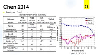
This document summarizes several papers on distributed amplifier design. It begins with an introduction to distributed amplifiers and their advantages over lumped element designs for wideband applications. It then reviews several papers that propose different distributed amplifier architectures and gain cell designs to achieve high gain, low noise, and low power consumption. Simulation results are presented for each design showing improvements in metrics like gain bandwidth, noise figure, and power efficiency. The document concludes with references to papers on distributed amplifier research.


![RF Module Design - [Chapter 6] Power Amplifier](https://cdn.slidesharecdn.com/ss_thumbnails/rfch6-150613070347-lva1-app6891-thumbnail.jpg?width=640&height=640&fit=bounds)


![[Deck] What's New in Spark-Iceberg Integration via DSV2.pptx](https://cdn.slidesharecdn.com/ss_thumbnails/deckwhatsnewinspark-icebergintegrationviadsv2-260210005337-25955b12-thumbnail.jpg?width=640&height=640&fit=bounds)


