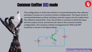
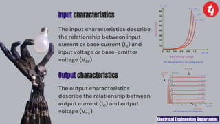
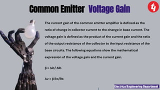
Download to read offline


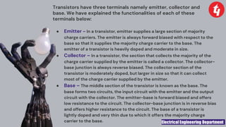


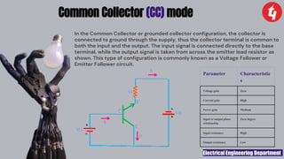

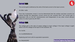

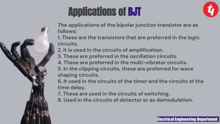


The document provides an overview of bipolar junction transistors (BJTs), detailing their construction, types (npn and pnp), and operational principles, including the key modes of operation: common base, common emitter, and common collector. It highlights the function and characteristics of the emitter, base, and collector terminals, as well as the voltage and current gains associated with each configuration. The applications of BJTs in amplification, switching, and circuit design are also discussed, emphasizing their significance in electronic circuits.


