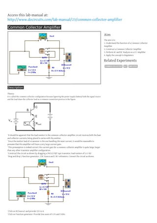
Access this lab-manual at:
http://www.docircuits.com/lab-manual/23/common-collector-amplifier
Common Collector Amplifier
Aim
The aim is to
1. Understand the function of a Common Collector
Amplifier
2. Construct a Common Collector Amplifier
3. Perform AC and DC Analysis on a CC Amplifier
4. Apply the concept to Regulators

Related Experiments
COMMON COLLECTOR

Description
Theory:
It is called the common collector configuration because (ignoring the power supply battery) both the signal source
and the load share the collector lead as a common connection point as in the figure.

¨It should be apparent that the load resistor in the common-collector amplifier circuit receives both the base
and collector currents, being placed in series with the emitter.
¨Since the emitter lead of a transistor is the one handling the most current, it would be reasonable to
presume that this amplifier will have a very large current gain.
¨This presumption is indeed correct: the current gain for a common-collector amplifier is quite large, larger
than any other transistor amplifier configuration.
¨Construct the circuit as shown by dragging a 2N2222 BJT npn transistor, load resistor of 5.11 KΩ
¨Drag and drop 1 function generator, 1 DC Source and 2 DC voltmeters. Connect the circuit as shown.

¨Click on DCSource1 and provide 15V to it.
¨Click on Function generator. Provide Sine wave of 1.5V and 2 KHz.

BJT

AMPLIFIER
¨Click on Function generator. Provide Sine wave of 1.5V and 2 KHz.
¨Give Offset ( Bias ) of 2.3V.
¨Run Simulation ( Time Domain )
¨Click on Analyse to view results
¨Plot Oscilloscope over time

Conclusion
¨We can see that the output follows the input.
¨The output is the same peak-to-peak amplitude as the input. Though, the DC level is shifted downward by
one VBE diode drop.

Common Collector Amplifier : BJT

  • 1.
    Access this lab-manualat: http://www.docircuits.com/lab-manual/23/common-collector-amplifier Common Collector Amplifier Aim The aim is to 1. Understand the function of a Common Collector Amplifier 2. Construct a Common Collector Amplifier 3. Perform AC and DC Analysis on a CC Amplifier 4. Apply the concept to Regulators Related Experiments COMMON COLLECTOR Description Theory: It is called the common collector configuration because (ignoring the power supply battery) both the signal source and the load share the collector lead as a common connection point as in the figure. ¨It should be apparent that the load resistor in the common-collector amplifier circuit receives both the base and collector currents, being placed in series with the emitter. ¨Since the emitter lead of a transistor is the one handling the most current, it would be reasonable to presume that this amplifier will have a very large current gain. ¨This presumption is indeed correct: the current gain for a common-collector amplifier is quite large, larger than any other transistor amplifier configuration. ¨Construct the circuit as shown by dragging a 2N2222 BJT npn transistor, load resistor of 5.11 KΩ ¨Drag and drop 1 function generator, 1 DC Source and 2 DC voltmeters. Connect the circuit as shown. ¨Click on DCSource1 and provide 15V to it. ¨Click on Function generator. Provide Sine wave of 1.5V and 2 KHz. BJT AMPLIFIER
  • 2.
    ¨Click on Functiongenerator. Provide Sine wave of 1.5V and 2 KHz. ¨Give Offset ( Bias ) of 2.3V. ¨Run Simulation ( Time Domain ) ¨Click on Analyse to view results ¨Plot Oscilloscope over time Conclusion ¨We can see that the output follows the input. ¨The output is the same peak-to-peak amplitude as the input. Though, the DC level is shifted downward by one VBE diode drop.