Cmos fabrication is a part of semiconductor electronics that deals with the designing and fabrication process with NMOS and Cmos and other processes like Twin tub techniques and etc.
The CMOS fabrication process in VLSI.
CMOS (complementary metal-oxide-semiconductor) is the term usually used to describe the small amount of memory on a computer motherboard that stores the BIOS settings.
Semiconductor device fabrication is the process used to create the integrated circuits that are present in everyday electrical and electronic devices. It is a multiple-step sequence of photo lithographic and chemical processing steps during which electronic circuits are gradually created on a wafer made of pure semiconducting material. Silicon is almost always used, but various compound semiconductors are used for specialized applications.
In MOS, source-drain regions of adjacent MOS transistors together with interconnection metal lines may constitute parasitic MOS transistors unless they are isolated from each other. Hence, each MOSFET must be electrically isolated from each other. Device Isolation Techniques in VLSI microfabrication of MOS are discussed.
CMOS FABRICATION
For less power dissipation requirement CMOS technology is used for implementing transistors. If we require a faster circuit then transistors are implemented over IC using BJT . Fabrication of CMOS transistors as IC’s can be done in three different methods.
The N-well / P-well technology, where n-type diffusion is done over a p-type substrate or p-type diffusion is done over n-type substrate respectively.
P-WELL PROCESS
The fabrication steps of p well process are same as that of an n-well process except that instead of n-well a p-well is implanted . The process steps involved in p-well process are shown in Figure below. The process starts with the n type substrate
Floating Gate Devices are widely used in ROM based memories. In EEPROM, one such Floating gate MOS device FLOTOX is used. FLOTOX(Floating Gate Tunneling Oxide MOS) works on FN tunneling phenomenon. This presentation discusses the method for fabrication of such FLOTOX device(actually a EEPROM cell).
MONOLITHIC IC PROCESSES A monolithic integrated circuit (IC) is a set of circuitry on a single semiconductor plate or chip rather than built of separate elements as a discrete circuit is.
Sachpazis:Terzaghi Bearing Capacity Estimation in simple terms with Calculati...Dr.Costas Sachpazis
Terzaghi's soil bearing capacity theory, developed by Karl Terzaghi, is a fundamental principle in geotechnical engineering used to determine the bearing capacity of shallow foundations. This theory provides a method to calculate the ultimate bearing capacity of soil, which is the maximum load per unit area that the soil can support without undergoing shear failure. The Calculation HTML Code included.
Hierarchical Digital Twin of a Naval Power SystemKerry Sado
A hierarchical digital twin of a Naval DC power system has been developed and experimentally verified. Similar to other state-of-the-art digital twins, this technology creates a digital replica of the physical system executed in real-time or faster, which can modify hardware controls. However, its advantage stems from distributing computational efforts by utilizing a hierarchical structure composed of lower-level digital twin blocks and a higher-level system digital twin. Each digital twin block is associated with a physical subsystem of the hardware and communicates with a singular system digital twin, which creates a system-level response. By extracting information from each level of the hierarchy, power system controls of the hardware were reconfigured autonomously. This hierarchical digital twin development offers several advantages over other digital twins, particularly in the field of naval power systems. The hierarchical structure allows for greater computational efficiency and scalability while the ability to autonomously reconfigure hardware controls offers increased flexibility and responsiveness. The hierarchical decomposition and models utilized were well aligned with the physical twin, as indicated by the maximum deviations between the developed digital twin hierarchy and the hardware.
Overview of the fundamental roles in Hydropower generation and the components involved in wider Electrical Engineering.
This paper presents the design and construction of hydroelectric dams from the hydrologist’s survey of the valley before construction, all aspects and involved disciplines, fluid dynamics, structural engineering, generation and mains frequency regulation to the very transmission of power through the network in the United Kingdom.
Author: Robbie Edward Sayers
Collaborators and co editors: Charlie Sims and Connor Healey.
(C) 2024 Robbie E. Sayers
Welcome to WIPAC Monthly the magazine brought to you by the LinkedIn Group Water Industry Process Automation & Control.
In this month's edition, along with this month's industry news to celebrate the 13 years since the group was created we have articles including
A case study of the used of Advanced Process Control at the Wastewater Treatment works at Lleida in Spain
A look back on an article on smart wastewater networks in order to see how the industry has measured up in the interim around the adoption of Digital Transformation in the Water Industry.
Final project report on grocery store management system..pdfKamal Acharya
In today’s fast-changing business environment, it’s extremely important to be able to respond to client needs in the most effective and timely manner. If your customers wish to see your business online and have instant access to your products or services.
Online Grocery Store is an e-commerce website, which retails various grocery products. This project allows viewing various products available enables registered users to purchase desired products instantly using Paytm, UPI payment processor (Instant Pay) and also can place order by using Cash on Delivery (Pay Later) option. This project provides an easy access to Administrators and Managers to view orders placed using Pay Later and Instant Pay options.
In order to develop an e-commerce website, a number of Technologies must be studied and understood. These include multi-tiered architecture, server and client-side scripting techniques, implementation technologies, programming language (such as PHP, HTML, CSS, JavaScript) and MySQL relational databases. This is a project with the objective to develop a basic website where a consumer is provided with a shopping cart website and also to know about the technologies used to develop such a website.
This document will discuss each of the underlying technologies to create and implement an e- commerce website.
Gen AI Study Jams _ For the GDSC Leads in India.pdf
FABRICATION PROCESS
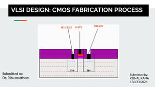
1. VLSI DESIGN: CMOS FABRICATION PROCESS
Submitted to:
Dr. Ribu matthew.
Submitted by:
KUNAL RANA
18BEE10024
2. STEP 1:
● First we choose a substrate for Nmos fabrication.
● P-Type substrate is preferred for NMOS Transistor.
3. STEP 2:
● A layer of silicon dioxide (SiO2) typically 1 micrometer thick is grown all over the
surface of the wafer to protect the surface and provide a generally insulating
substrate on to which other layers may be deposited and patterned.
4. STEP 3:
● The Photolithography is done next.
● The surface is removed with photoresist which is deposited and spun to
achieve the even distribution.
5. STEP 4:
● A mask is placed on PR later. Which defines
where regions into diffusion is to take place
together with transmission channels. i.e.UV
light passed and the area exposed to light
gets hardened while keeping Others
unaffected
● The unaffected area is
etched away with underlying
thick OX i.e.The remaining
PR is removed
6. STEP 5:
● The remaining photoresist is removed and a thin layer of SiO2 is grown over
the entire chip surface and then poly silicon is deposited on the top of this to
form the gate structure.
● Further photoresist coating and masking allows the polysilicon to be patterned
and then the thin oxide is removed to expose areas into which n-type
impurities are to be diffused to form the source and drain.
8. STEP 7:
● The n-type impurities are diffused in the exposed p-substrate from source and
drain
● Diffusion is done by heating the water to a high temperature and passing gas
containing the desired n-type impurities over the surface.
9. STEP 8:
● Thick OX layer is grown and then by photo photolithography 'contact cuts' are
formed.
10. STEP 9:
● The whole chip then has metal (aluminium) deposited over its surface. This
metal layer is then masked and etched to form the required interconnection
pattern.