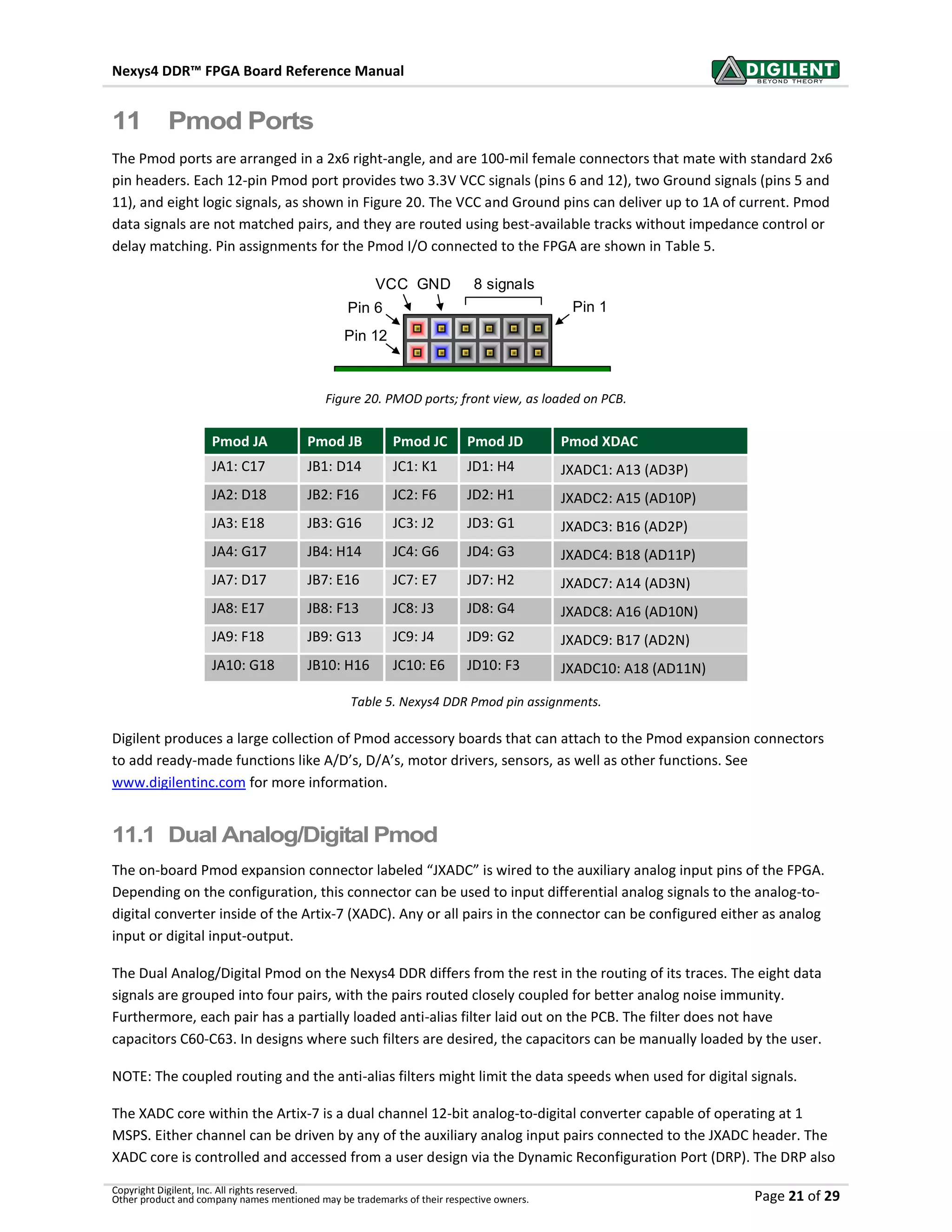
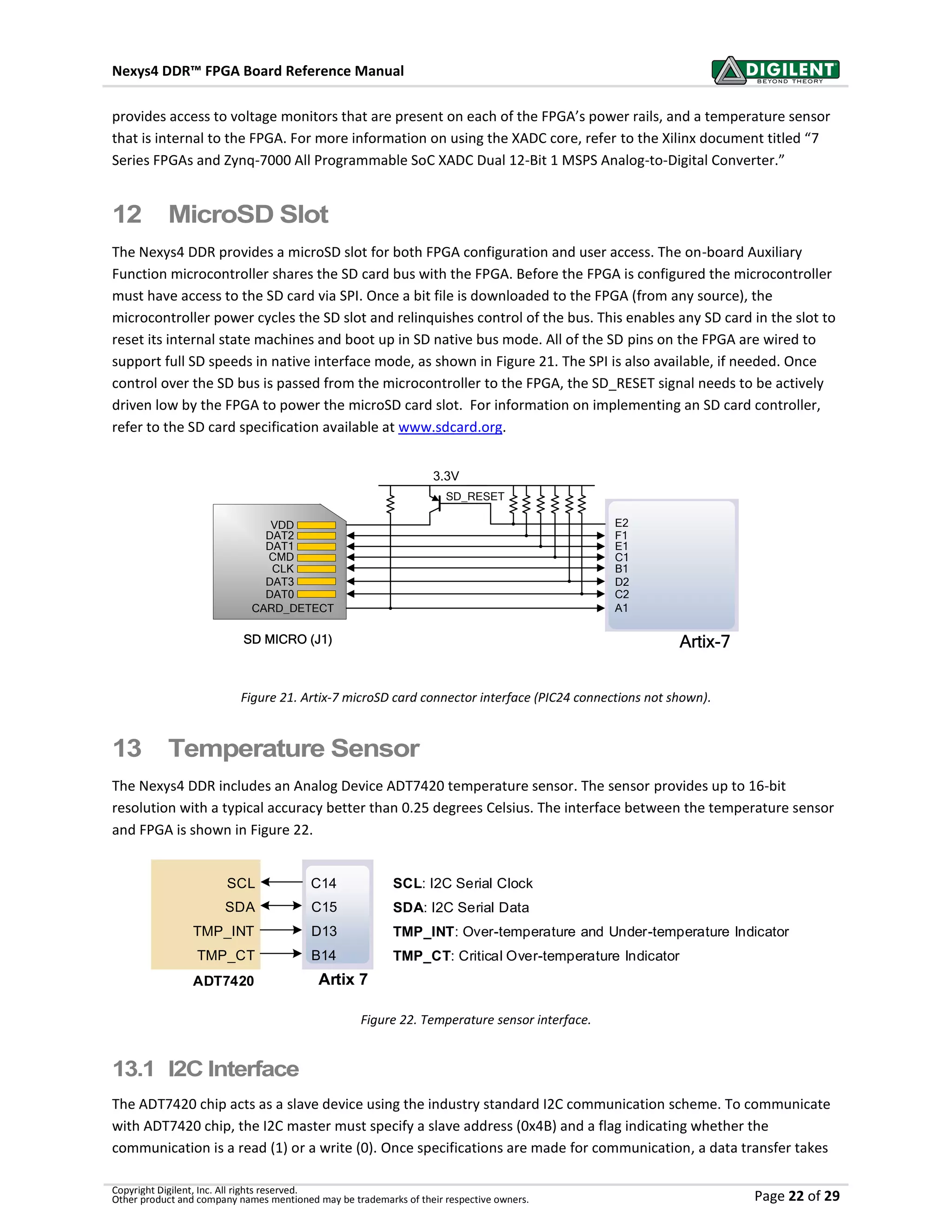
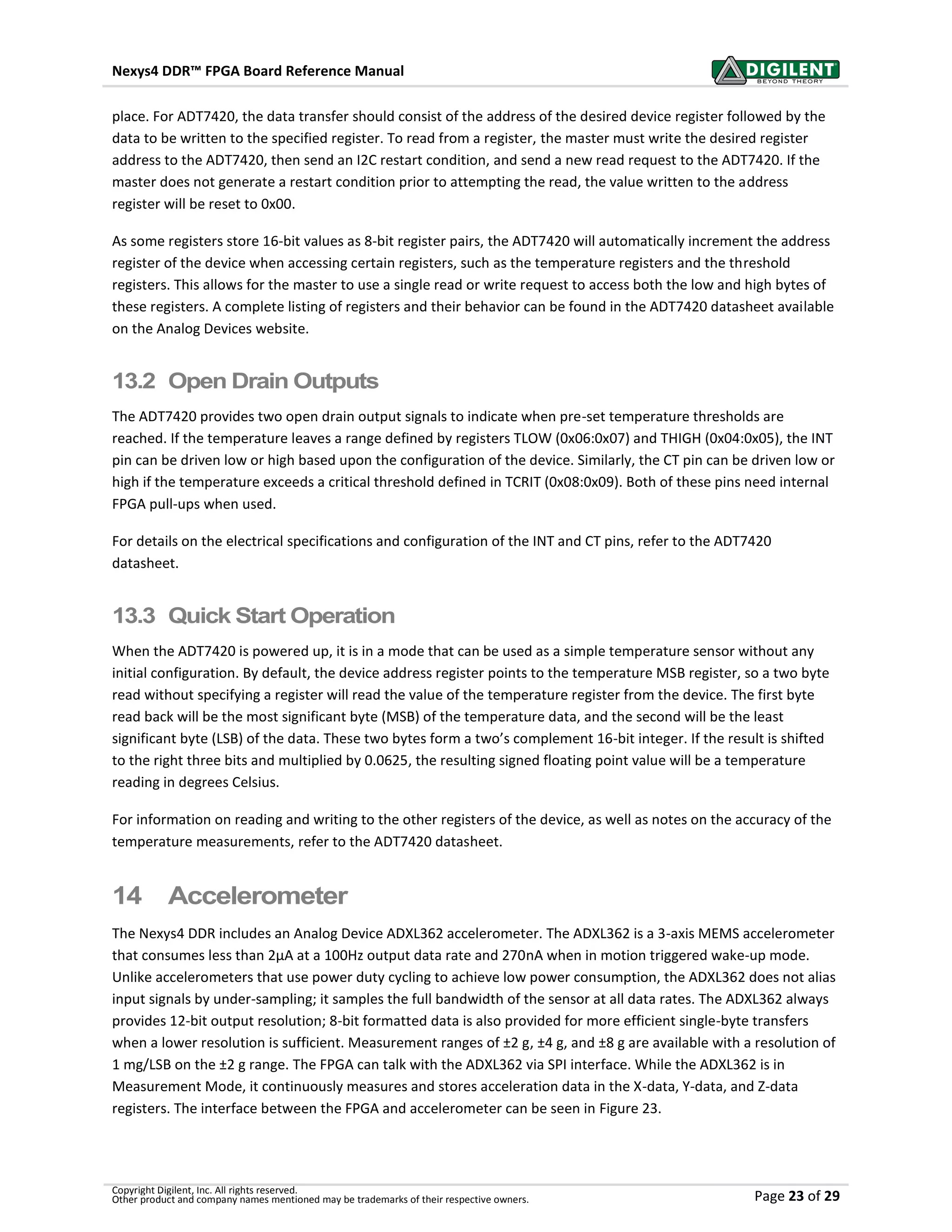
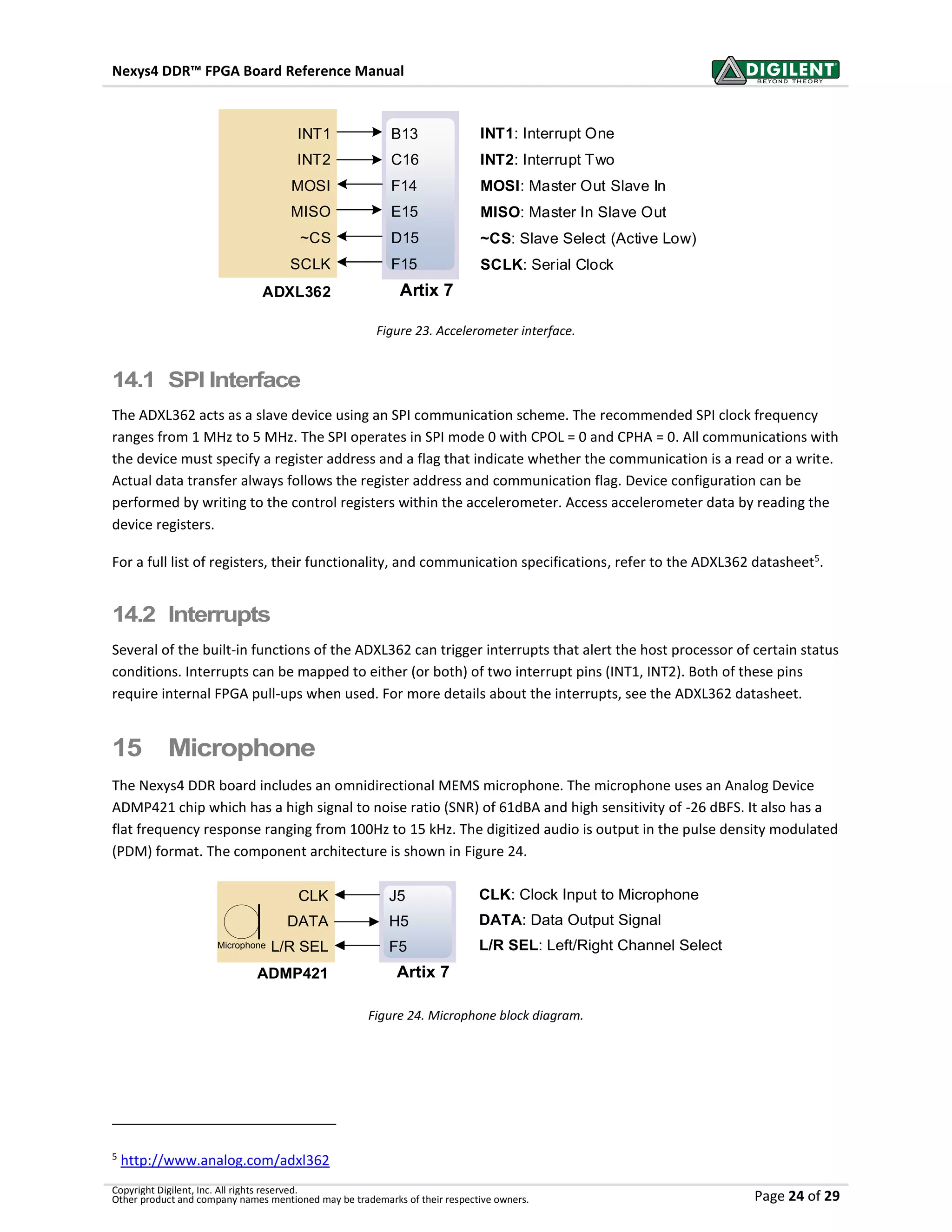
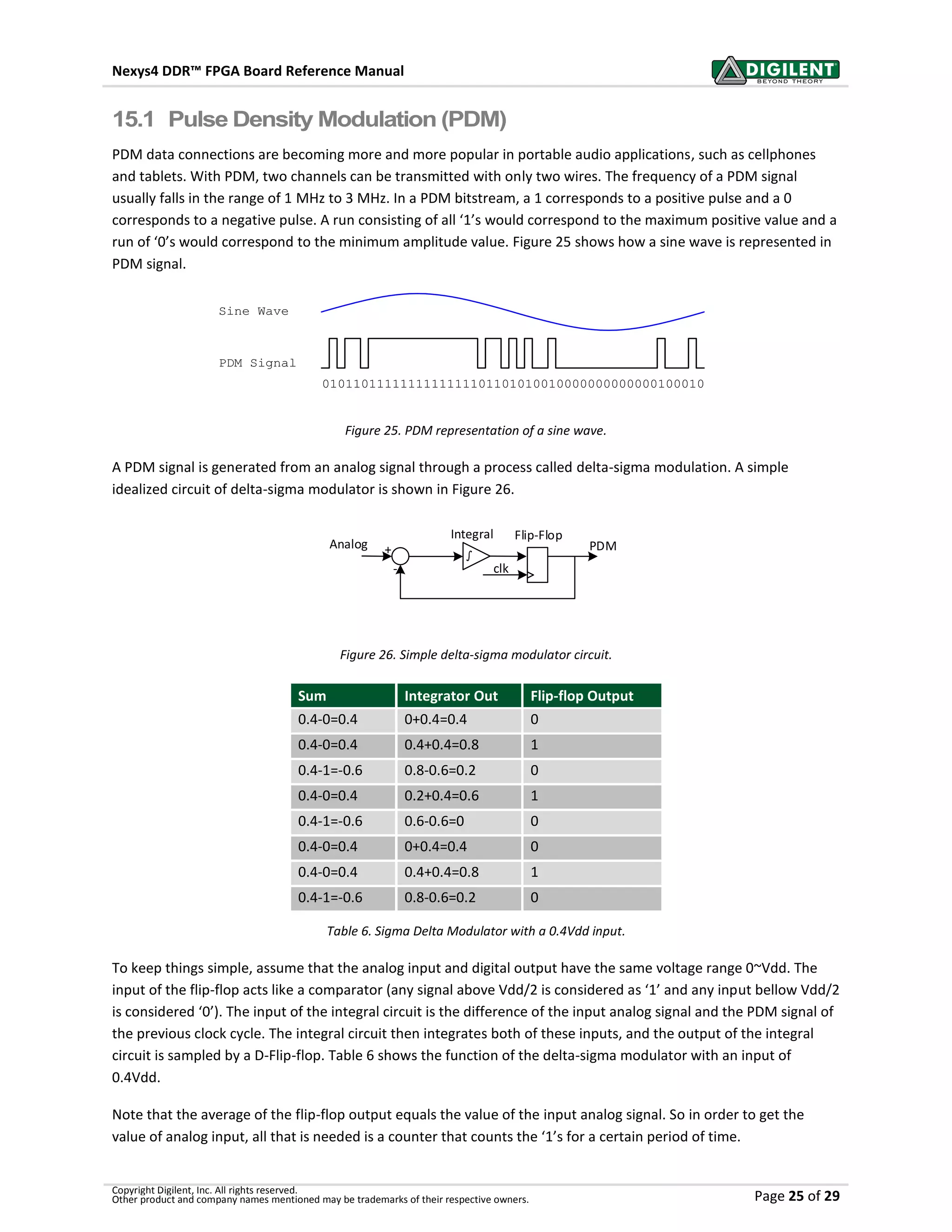
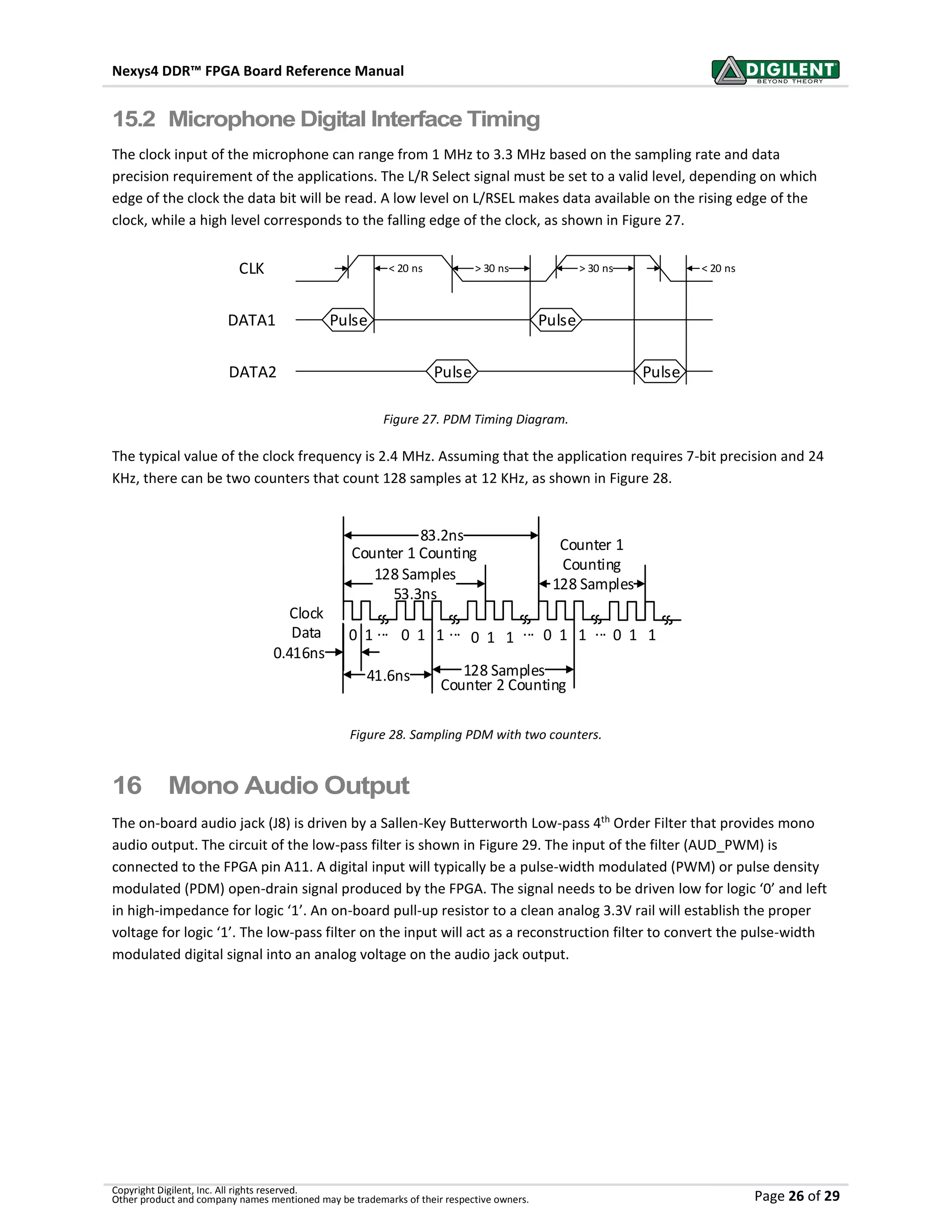
Download to read offline
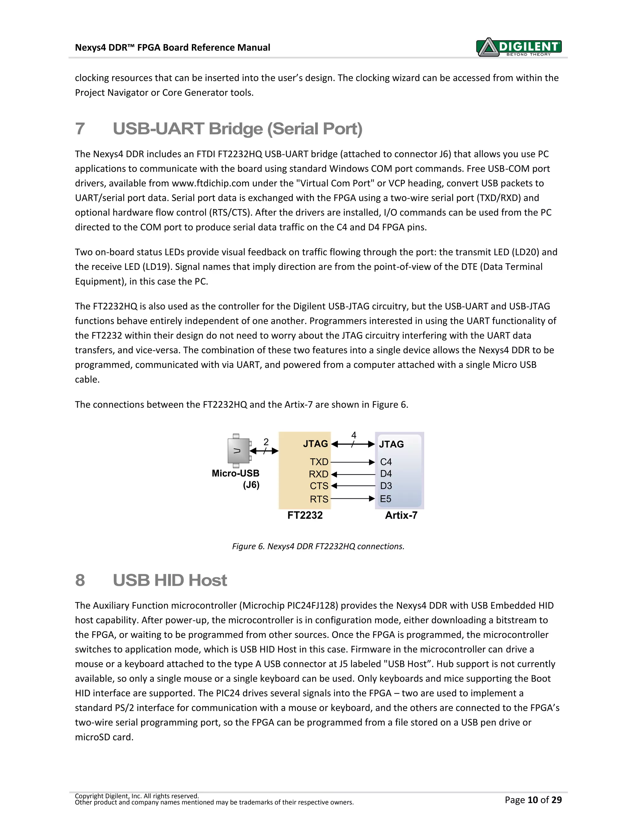
![Nexys4 DDR™ FPGA Board Reference Manual
Copyright Digilent, Inc. All rights reserved.
Other product and company names mentioned may be trademarks of their respective owners. Page 12 of 29
8.2 Keyboard
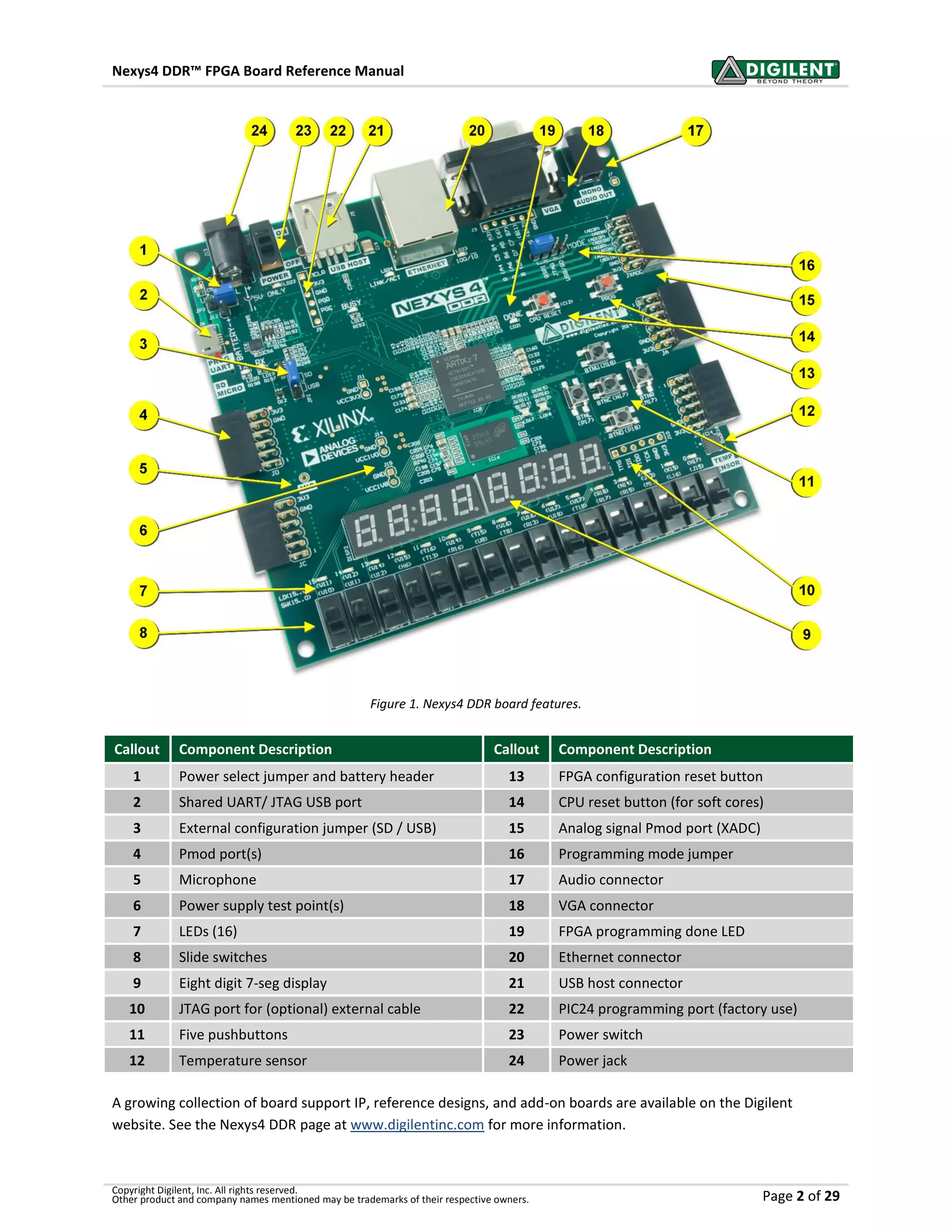
PS/2-style keyboards use scan codes to communicate key press data. Each key is assigned a code that is sent
whenever the key is pressed. If the key is held down, the scan code will be sent repeatedly about once every
100ms. When a key is released, an F0 key-up code is sent, followed by the scan code of the released key. If a key
can be shifted to produce a new character (like a capital letter), then a shift character is sent in addition to the scan
code and the host must determine which ASCII character to use. Some keys, called extended keys, send an E0
ahead of the scan code (and they may send more than one scan code). When an extended key is released, an E0 F0
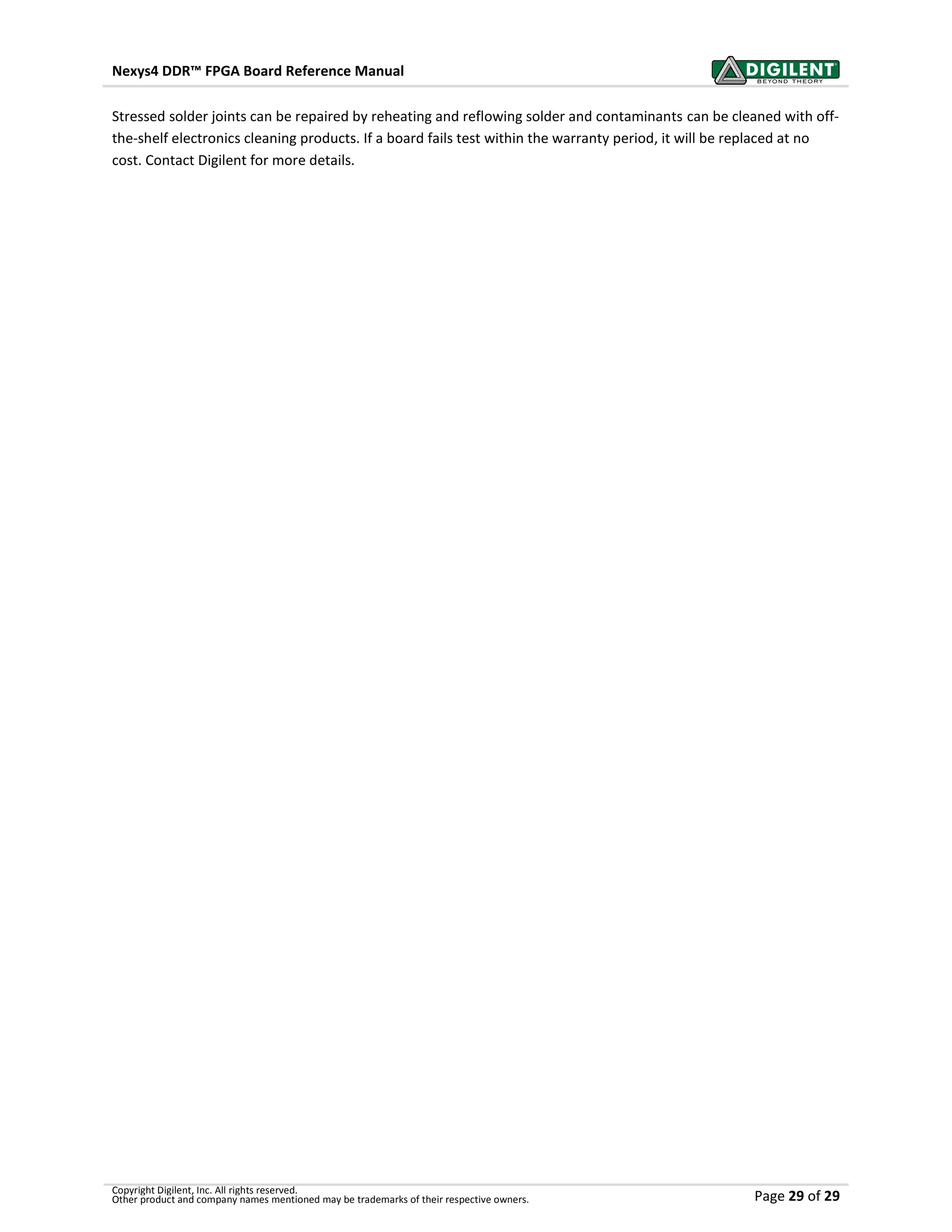
key-up code is sent, followed by the scan code. Scan codes for most keys are shown in Figure 9.
ESC
76
` ~
0E
TAB
0D
Caps Lock
58
Shift
12
Ctrl
14
1 !
16
2 @
1E
3 #
26
4 $
25
5 %
2E
Q
15
W
1D
E
24
R
2D
T
2C
A
1C
S
1B
D
23
F
2B
G
34
Z
1Z
X
22
C
21
V
2A
B
32
6 ^
36
7 &
3D
8 *
3E
9 (
46
0 )
45
- _
4E
= +
55
BackSpace
66
Y
35
U
3C
I
43
O
44
P
4D
[ {
54
] }
5B
|
5D
H
33
J
3B
K
42
L
4B
; :
4C
' "
52
Enter
5A
N
31
M
3A
, <
41
> .
49
/ ?
4A
Shift
59
Alt
11
Space
29
Alt
E0 11
Ctrl
E0 14
F1
05
F2
06
F3
04
F4
0C
F5
03
F6
0B
F7
83
F8
0A
F9
01
F10
09
F11
78
F12
07
Figure 9. Keyboard scan codes.
A host device can also send data to the keyboard. Table 3 shows a list of some common commands a host might
send.
The keyboard can send data to the host only when both the data and clock lines are high (or idle). Because the
host is the bus master, the keyboard must check to see whether the host is sending data before driving the bus. To
facilitate this, the clock line is used as a “clear to send” signal. If the host drives the clock line low, the keyboard
must not send any data until the clock is released. The keyboard sends data to the host in 11-bit words that
contain a ‘0’ start bit, followed by 8-bits of scan code (LSB first), followed by an odd parity bit, and terminated with
a ‘1’ stop bit. The keyboard generates 11 clock transitions (at 20 to 30 KHz) when the data is sent, and data is valid
on the falling edge of the clock.
Command Action
ED
Set Num Lock, Caps Lock, and Scroll Lock LEDs. Keyboard returns FA after receiving ED, then
host sends a byte to set LED status: bit 0 sets Scroll Lock, bit 1 sets Num Lock, and bit 2 sets
Caps lock. Bits 3 to 7 are ignored.
EE Echo (test). Keyboard returns EE after receiving EE
F3
Set scan code repeat rate. Keyboard returns F3 on receiving FA, then host sends second byte
to set the repeat rate.
FE Resend. FE directs keyboard to re-send most recent scan code.
FF Reset. Resets the keyboard.
Table 3. Keyboard commands.](https://image.slidesharecdn.com/nexys4ddrrm-191127151156/75/Nexys4ddr-rm-FPGA-board-Datasheet-12-2048.jpg)


This document provides an overview and reference manual for the Nexys4 DDR FPGA board. It describes the board's features such as the Artix-7 FPGA, memory resources, ports, and peripherals. It also provides details on power supplies, FPGA configuration options, and migrating designs from the original Nexys4 board. The manual is intended to help users understand and utilize the capabilities of the Nexys4 DDR board.