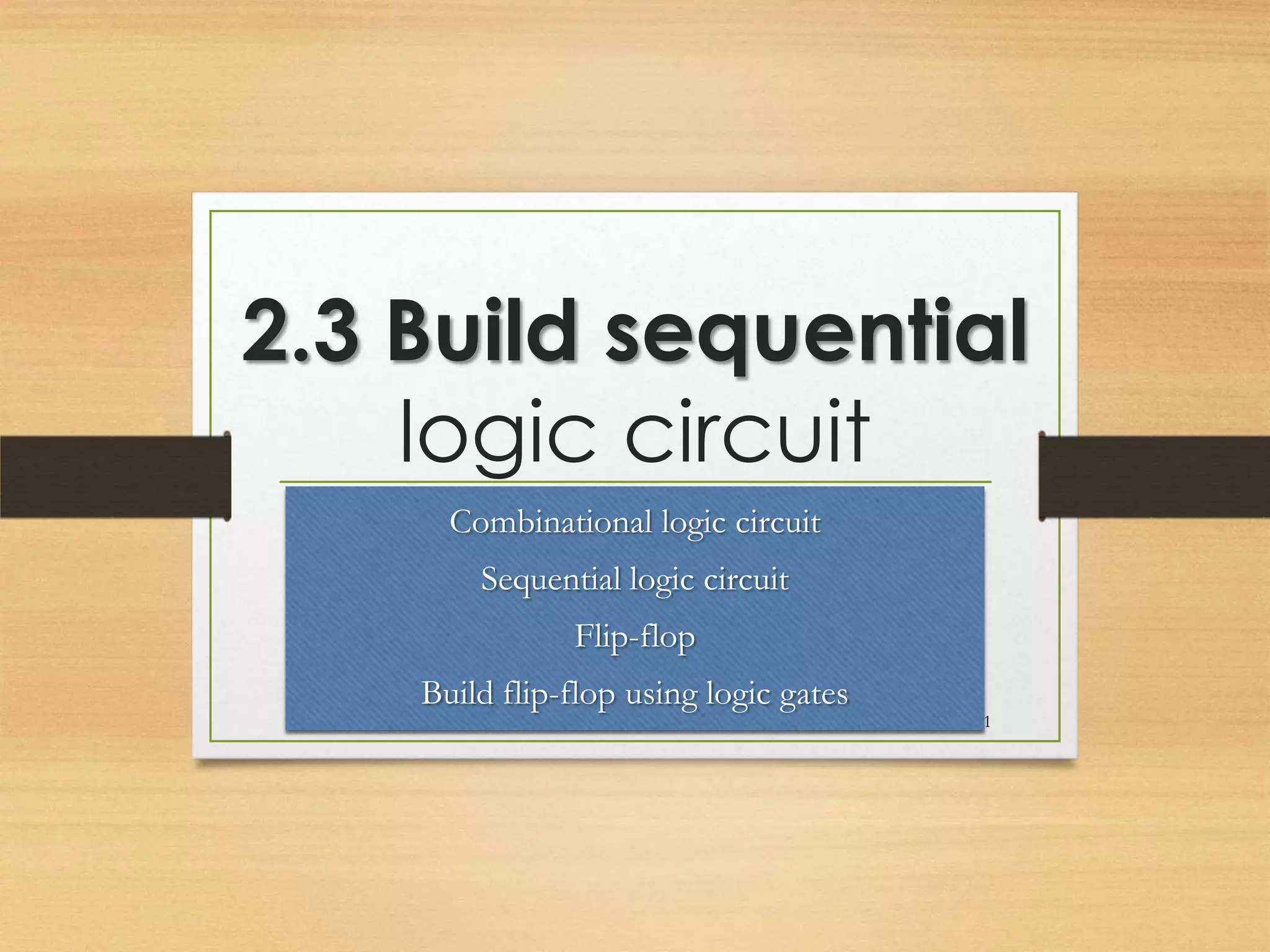
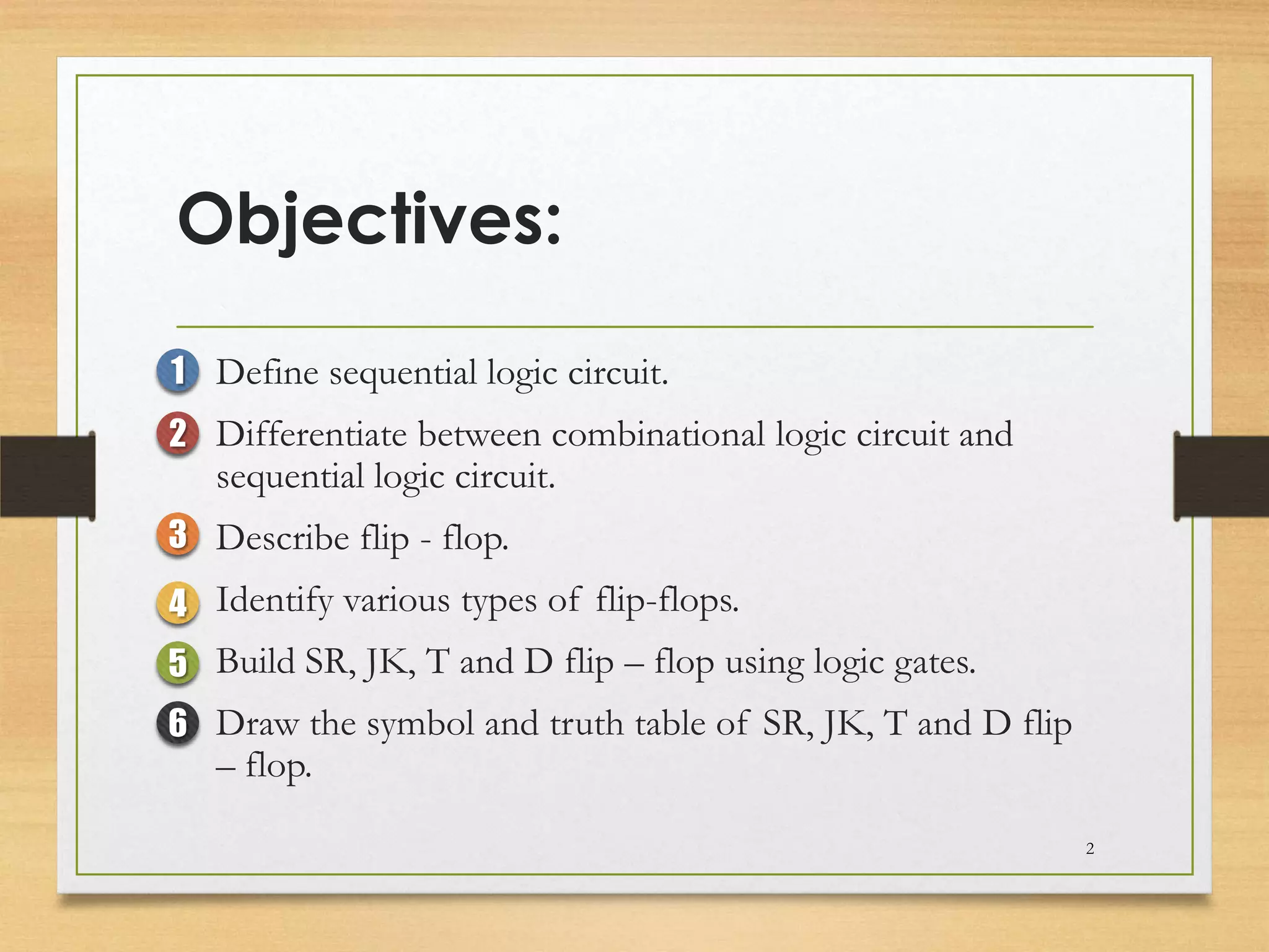
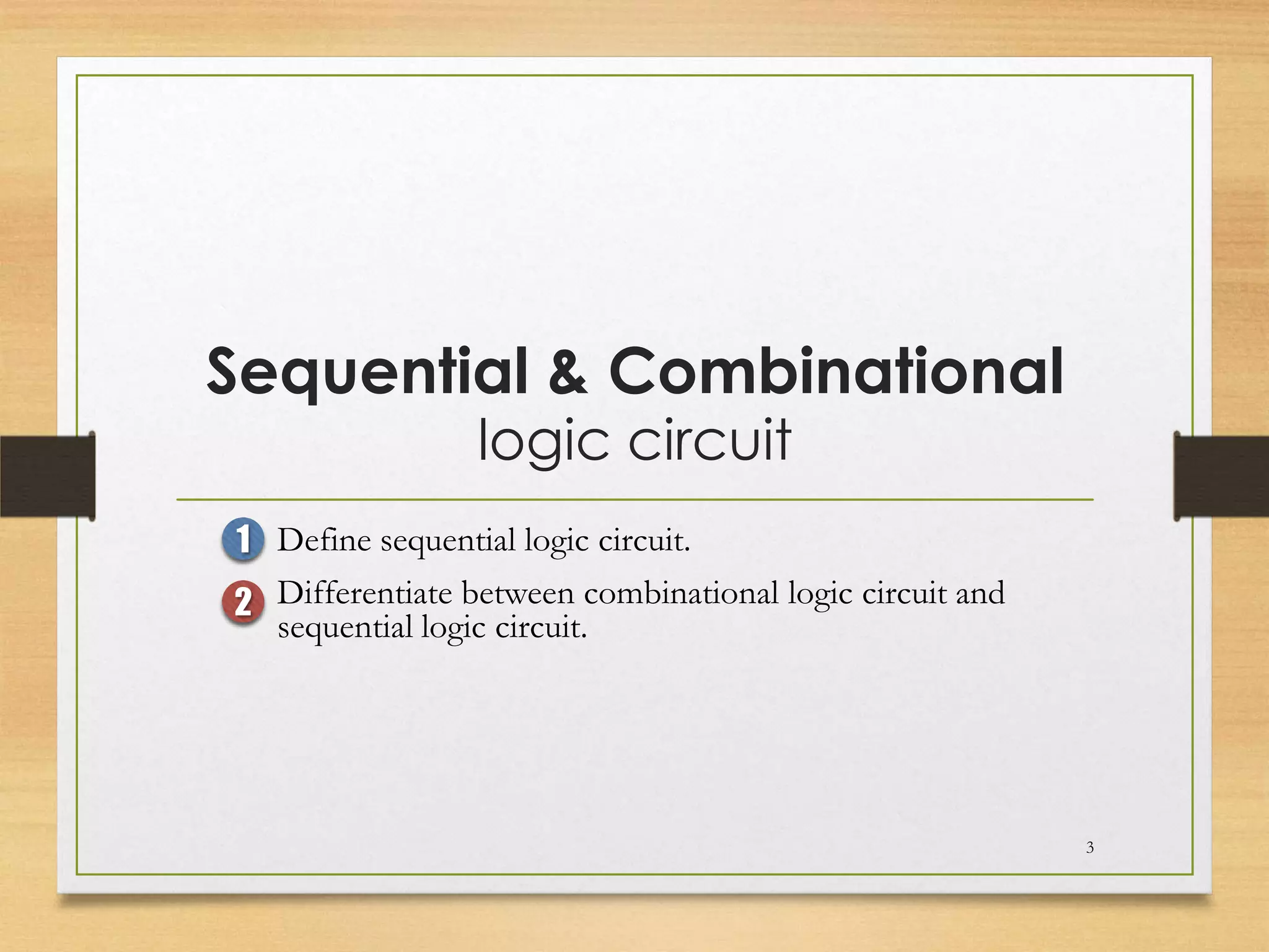
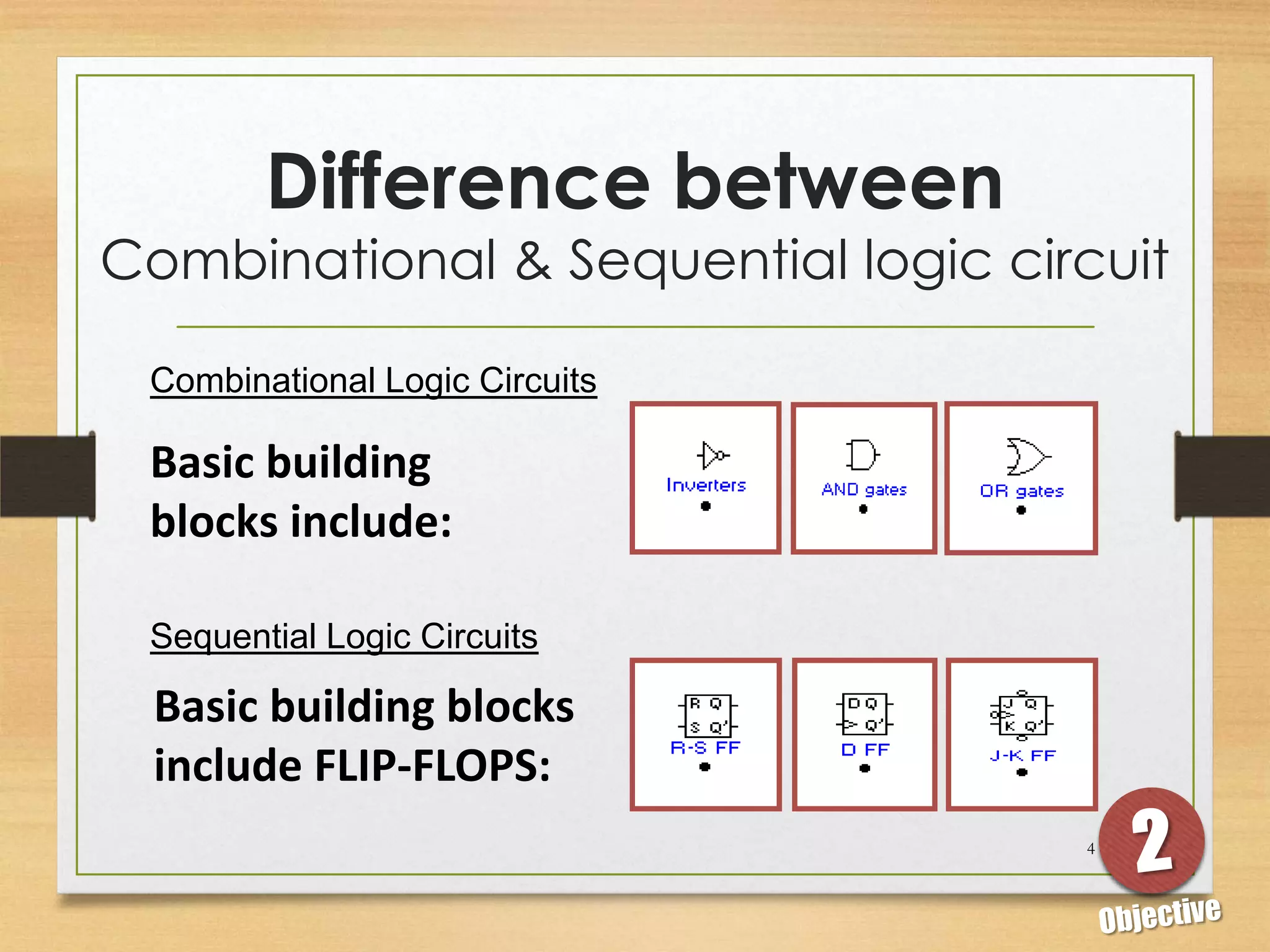
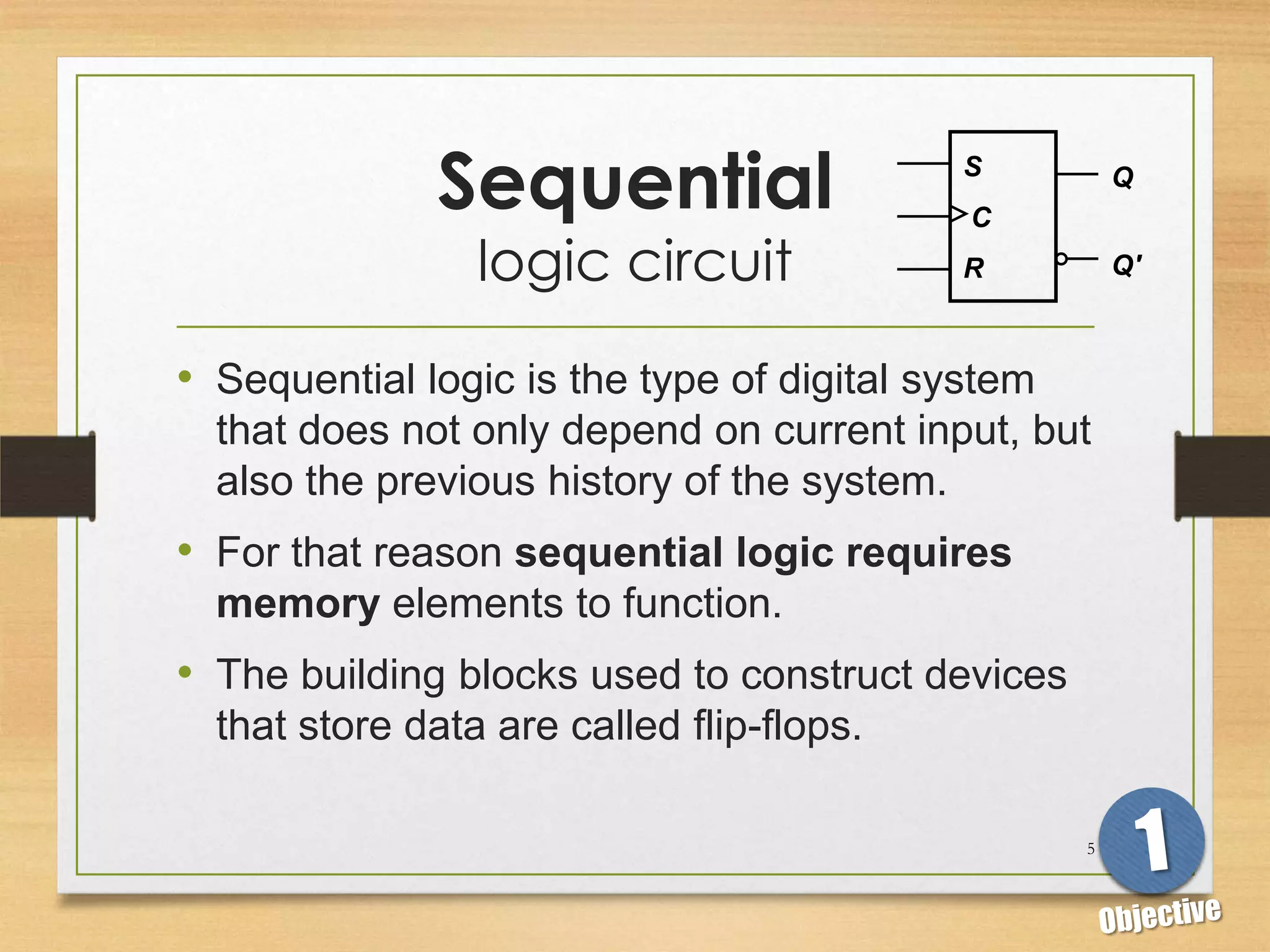
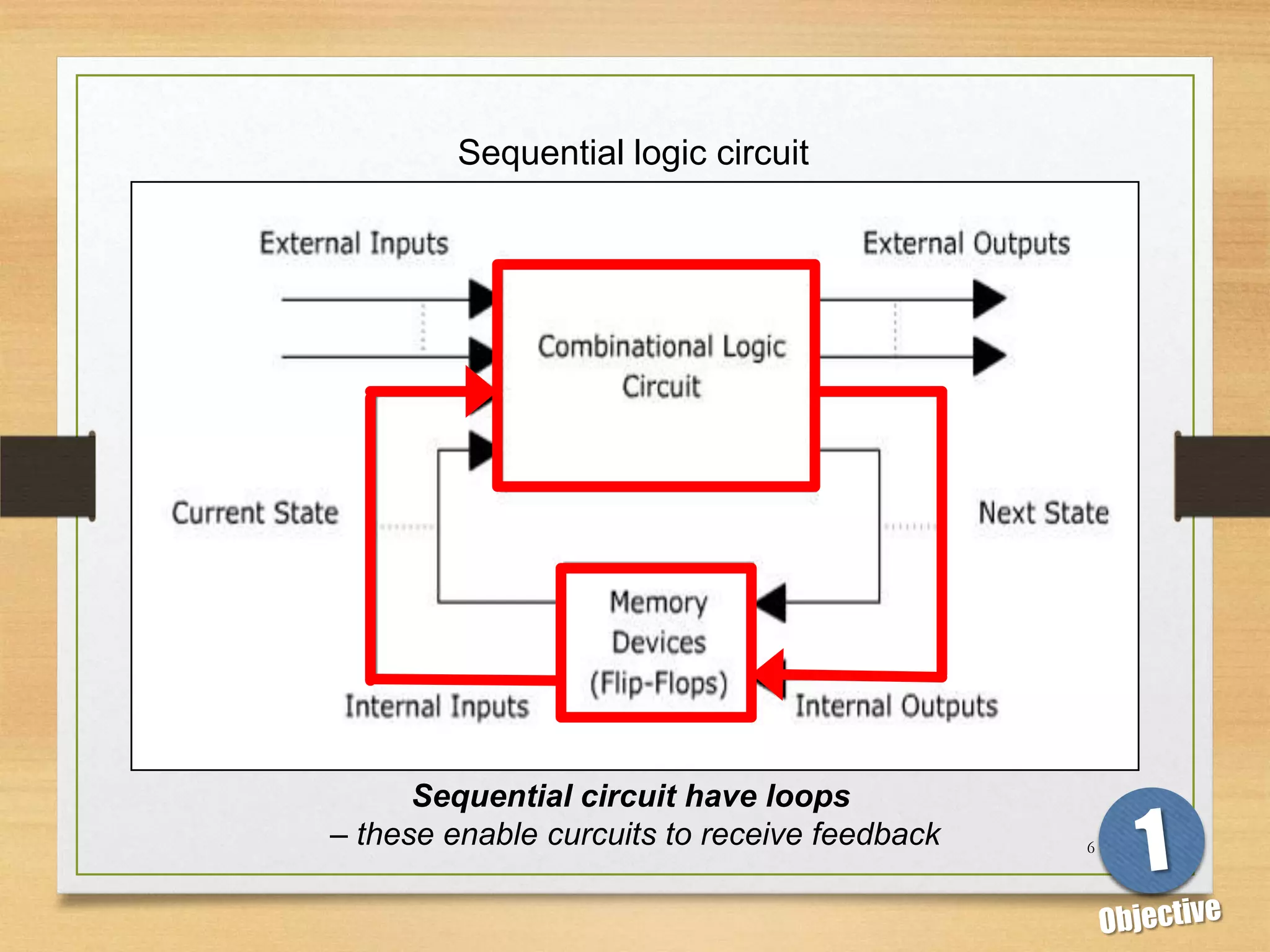
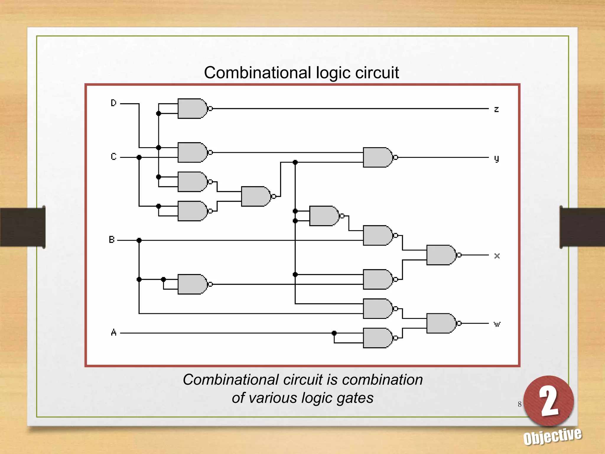
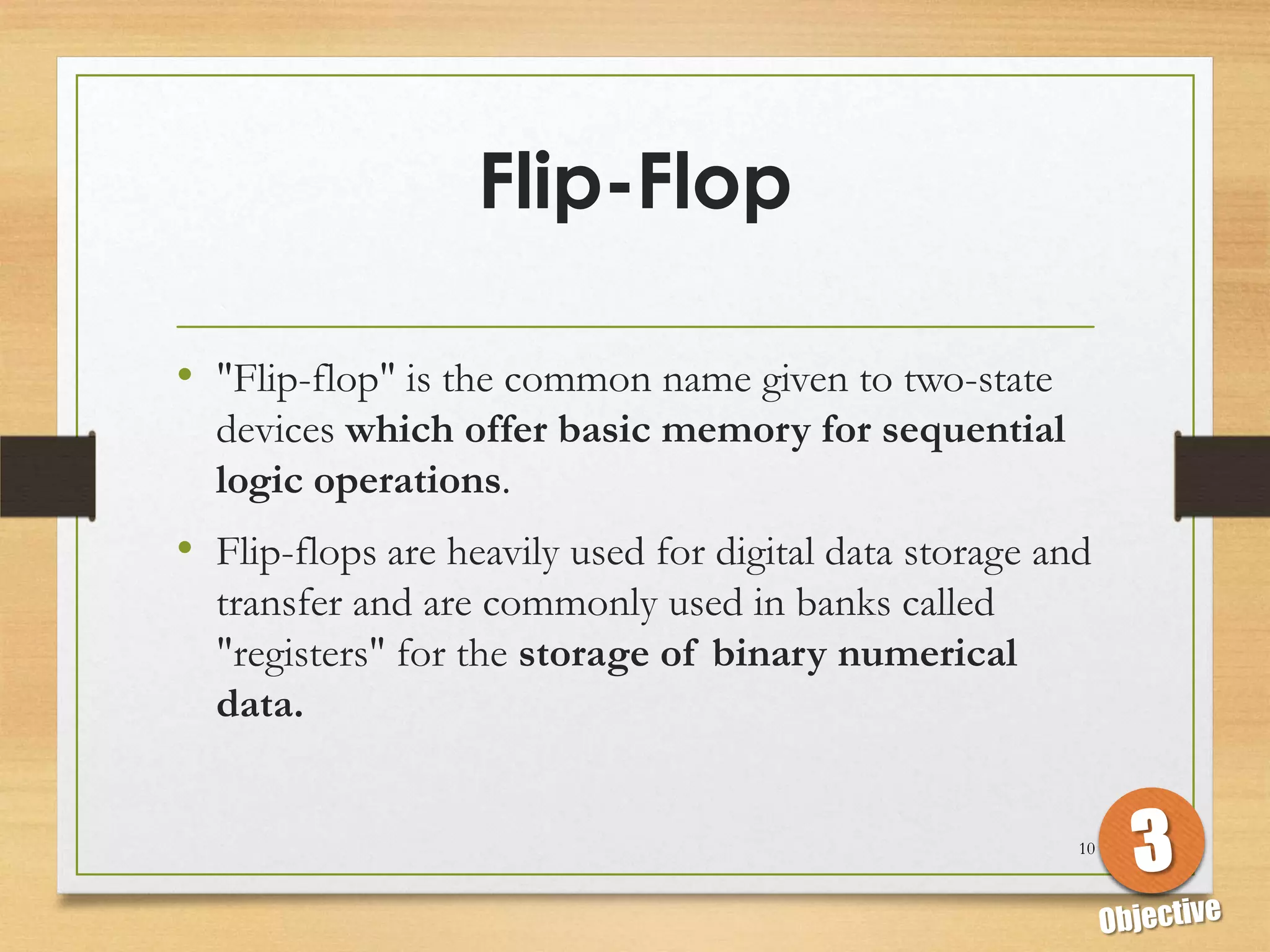
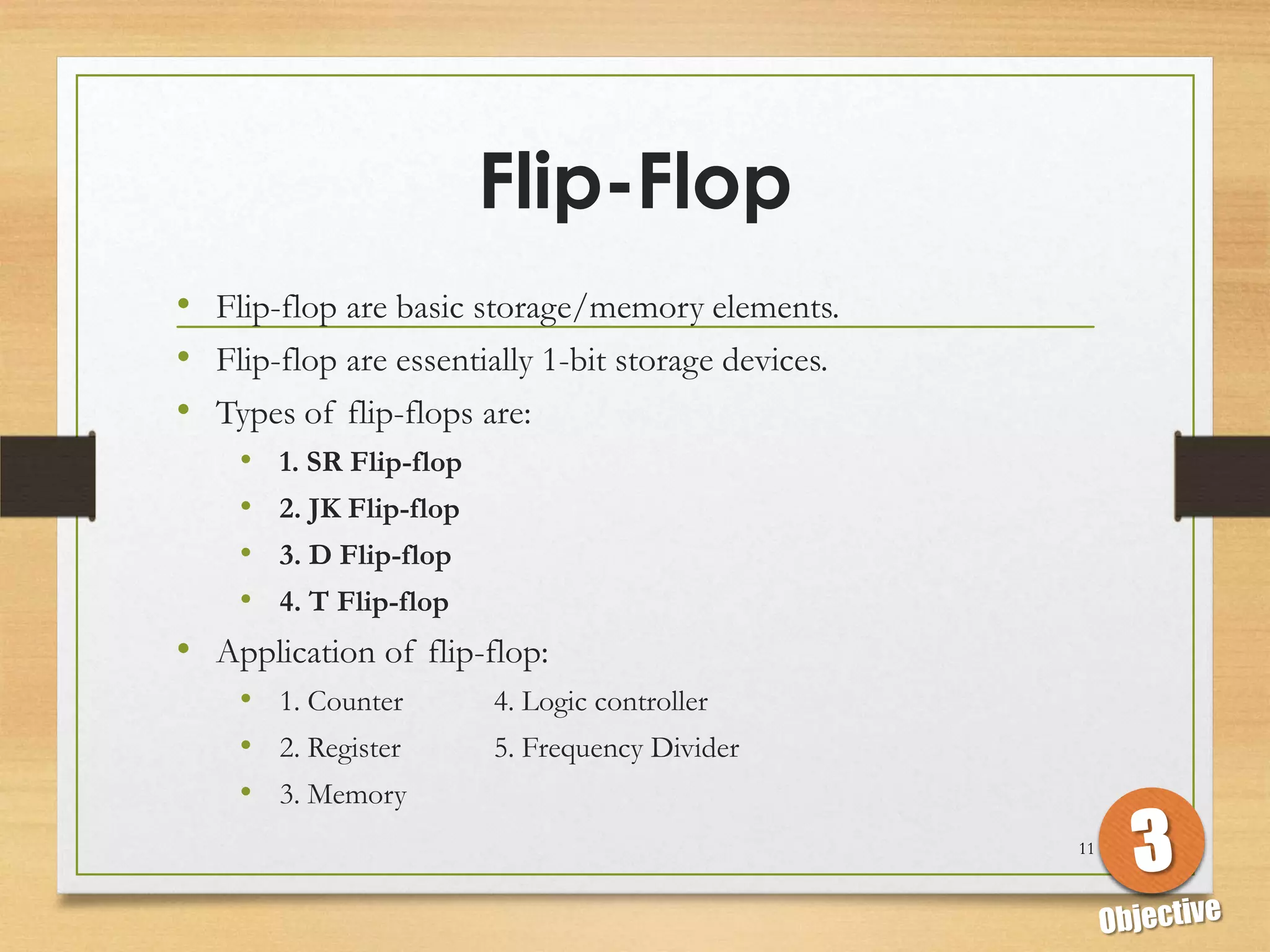
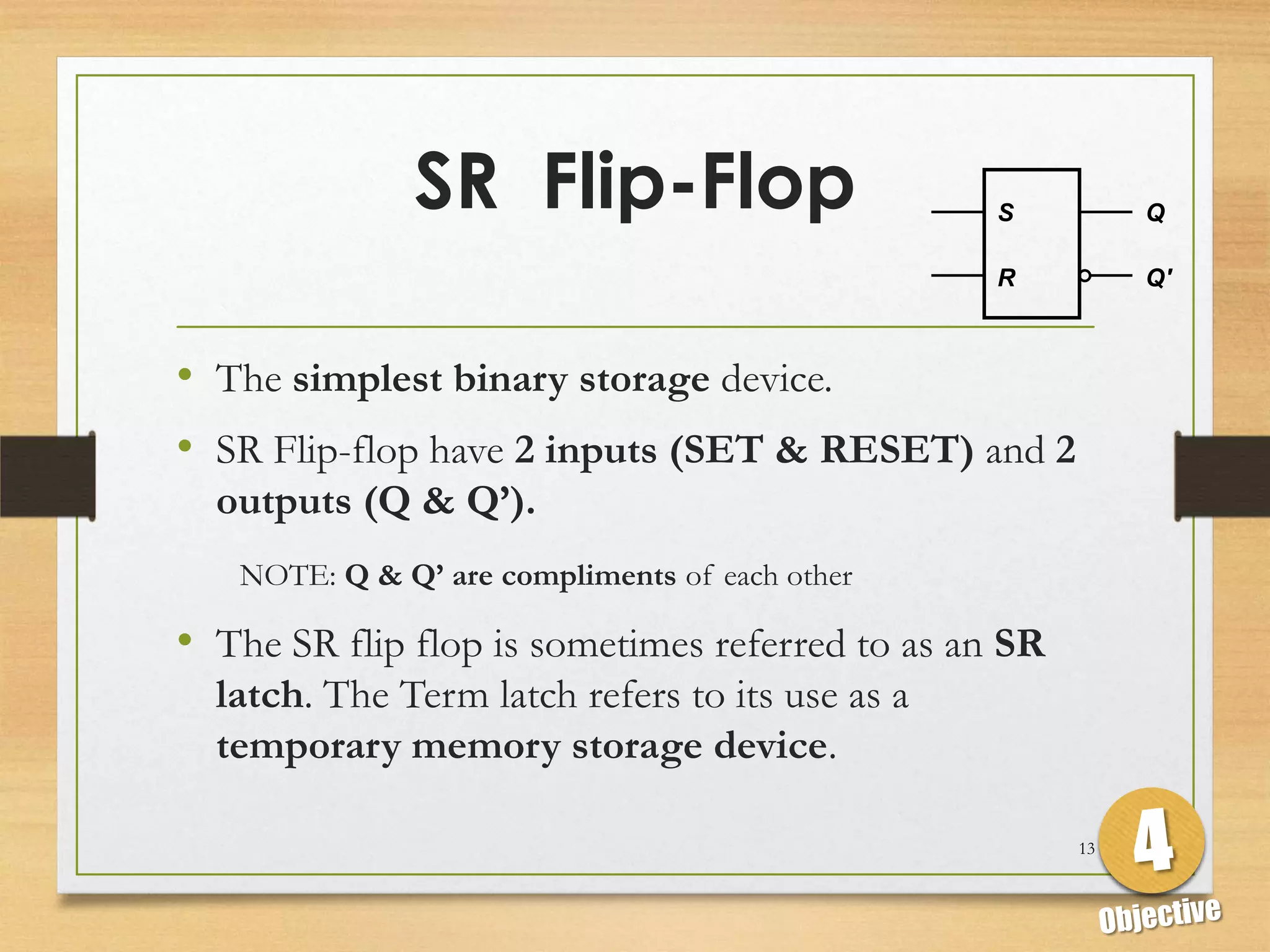
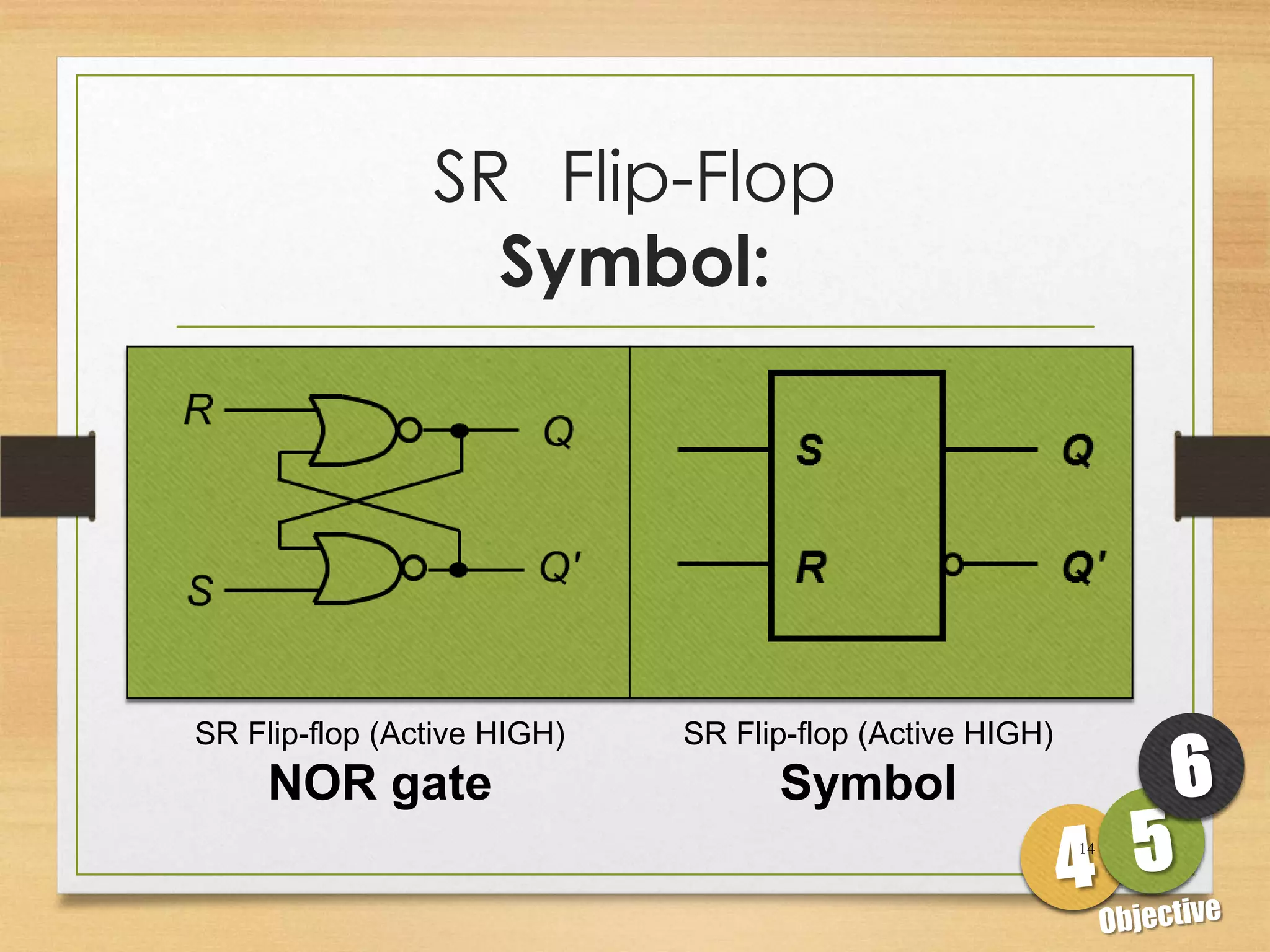
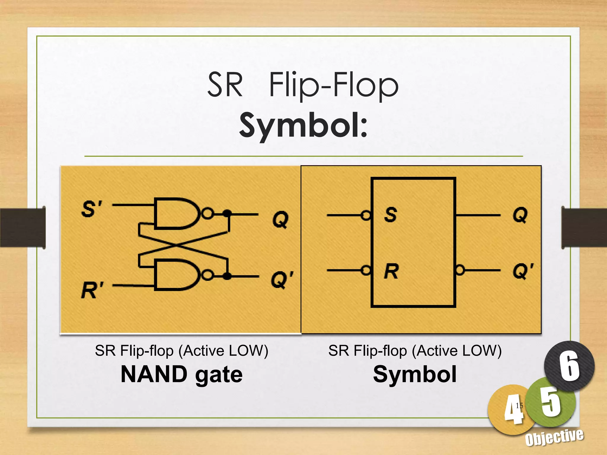
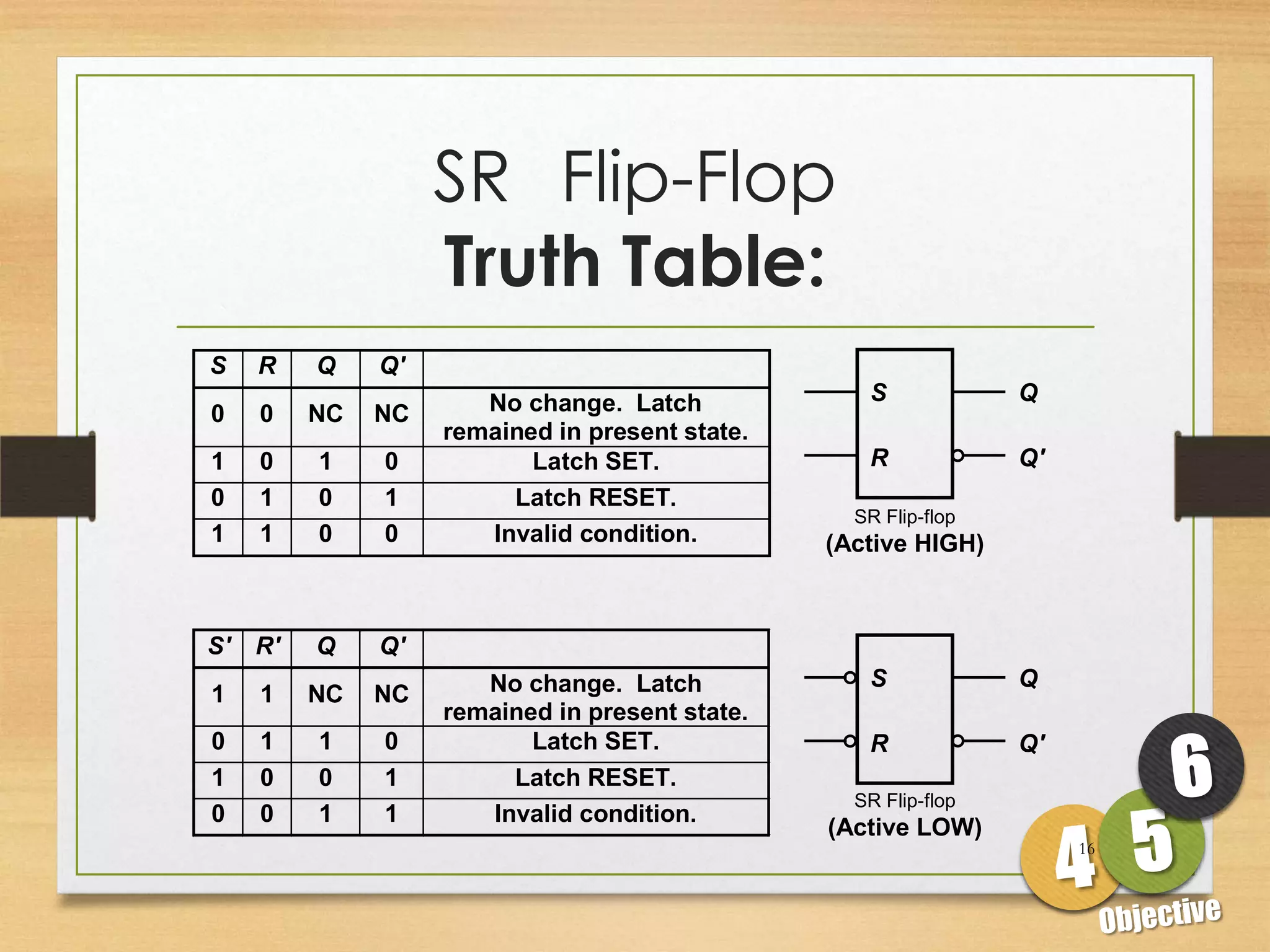
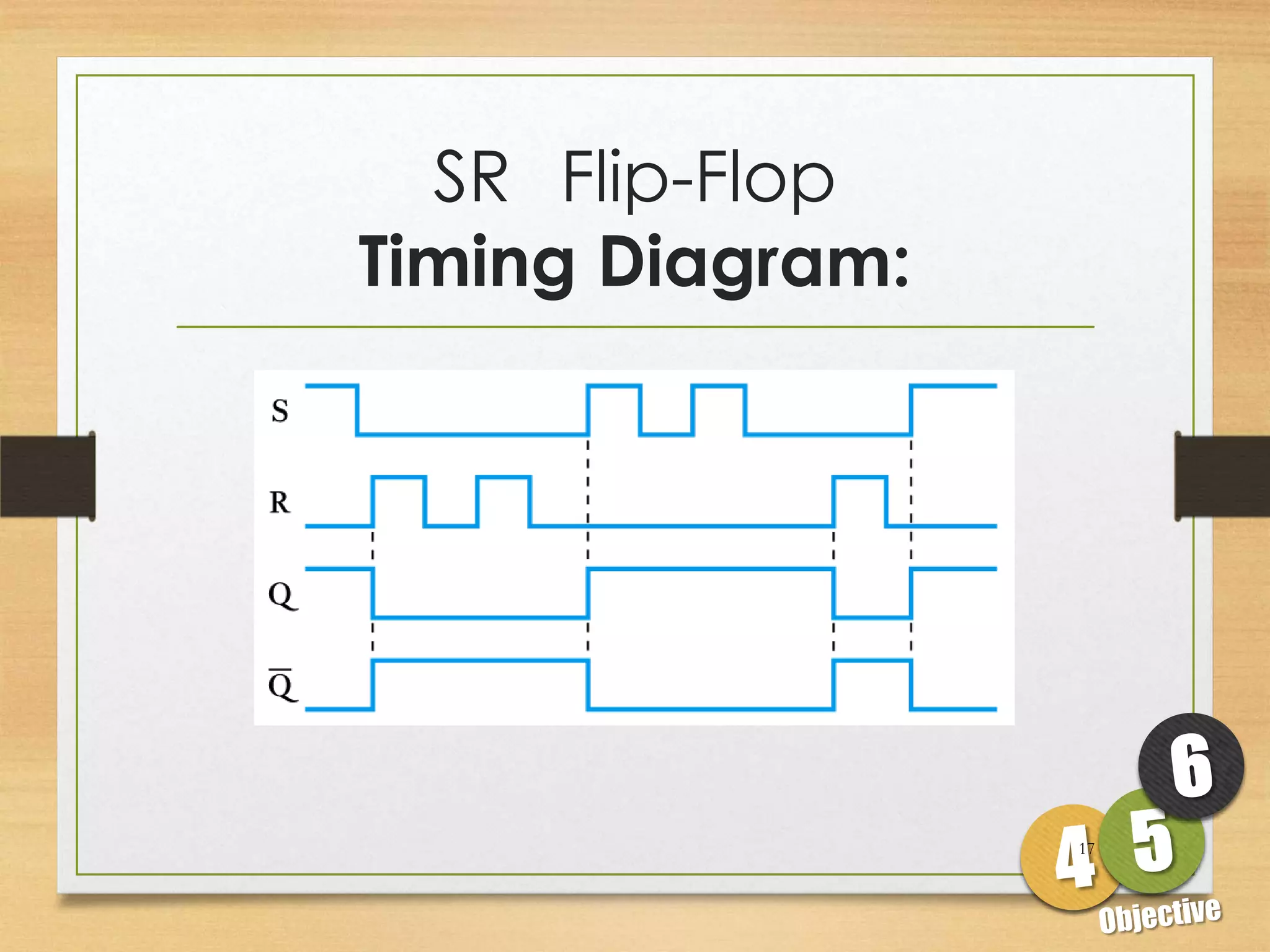
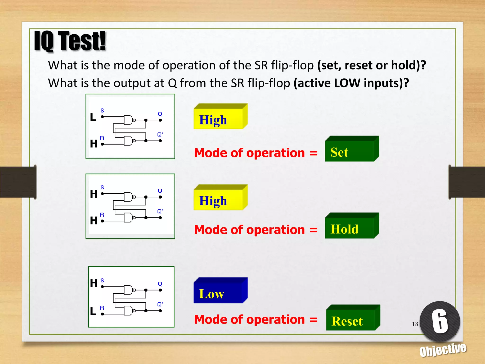
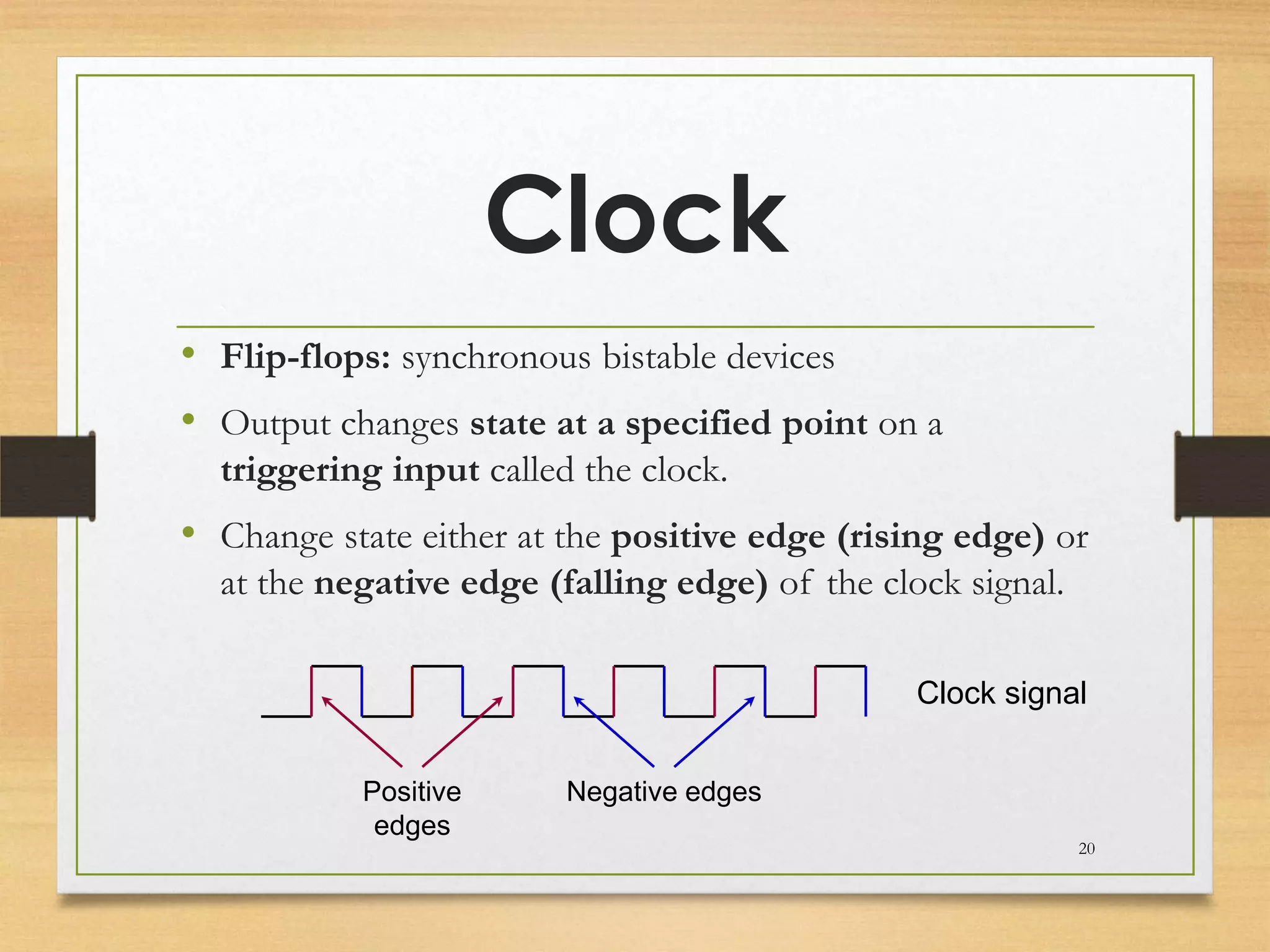
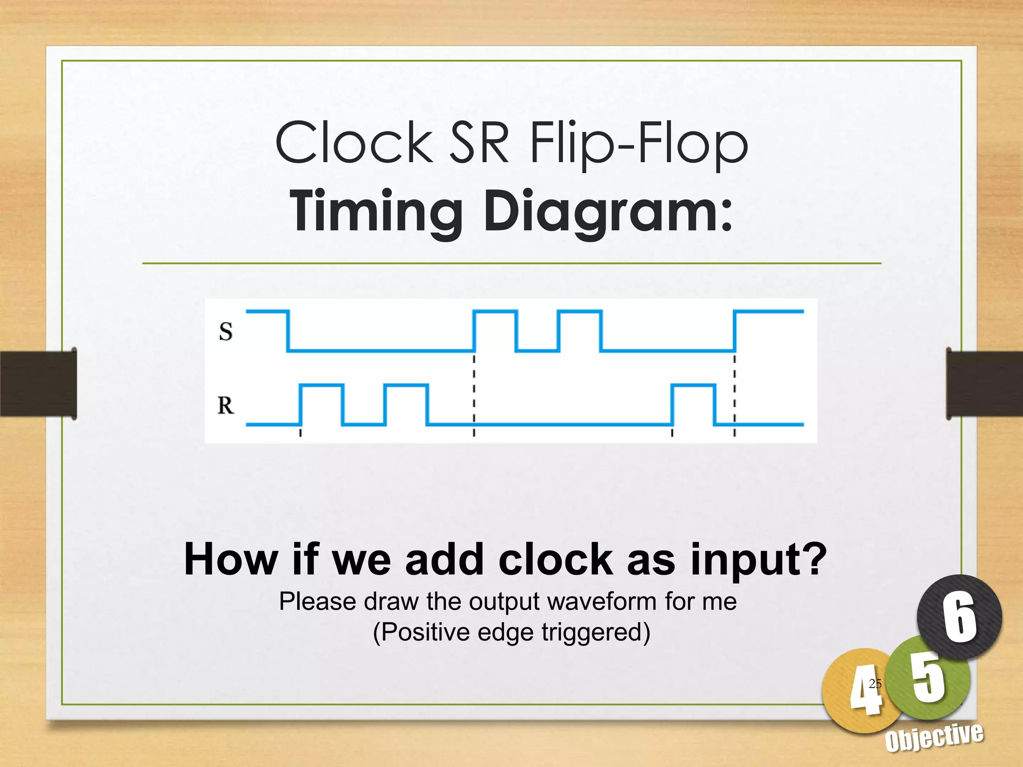
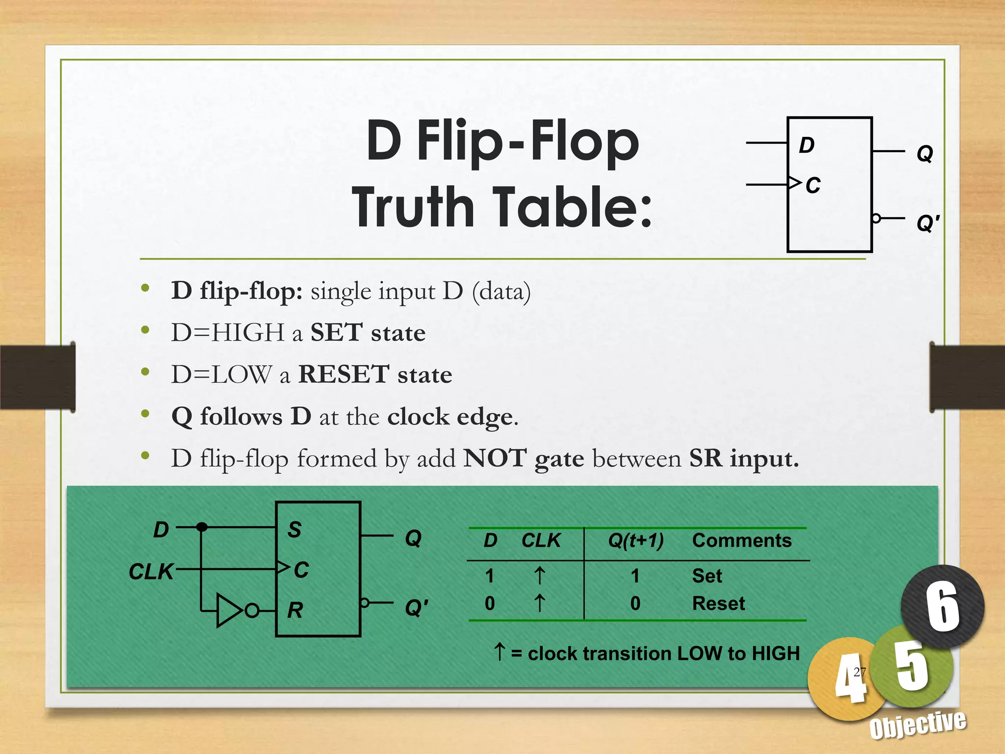
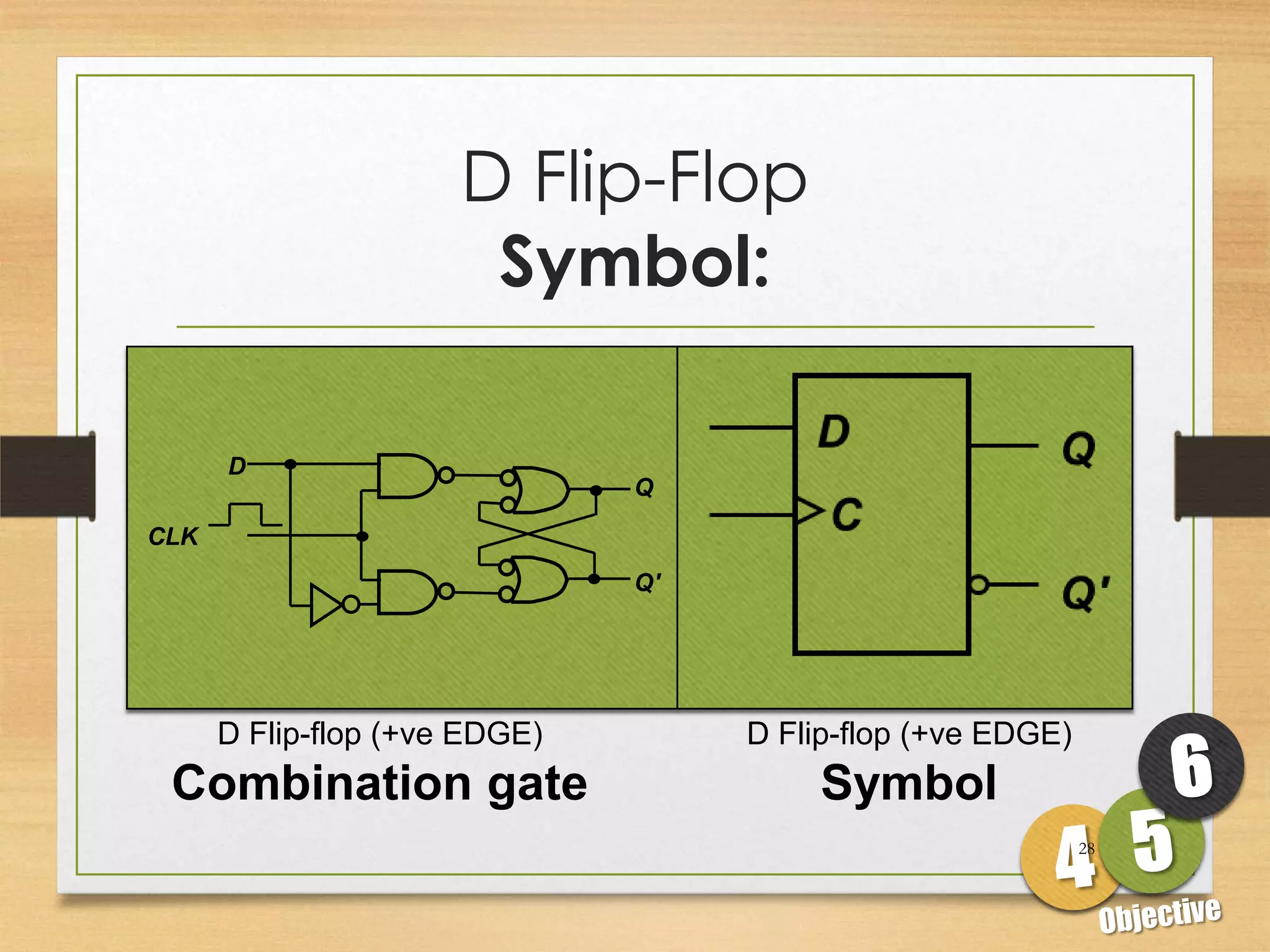
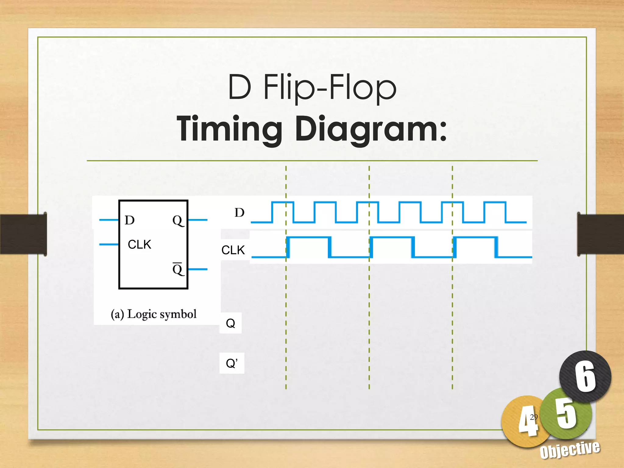
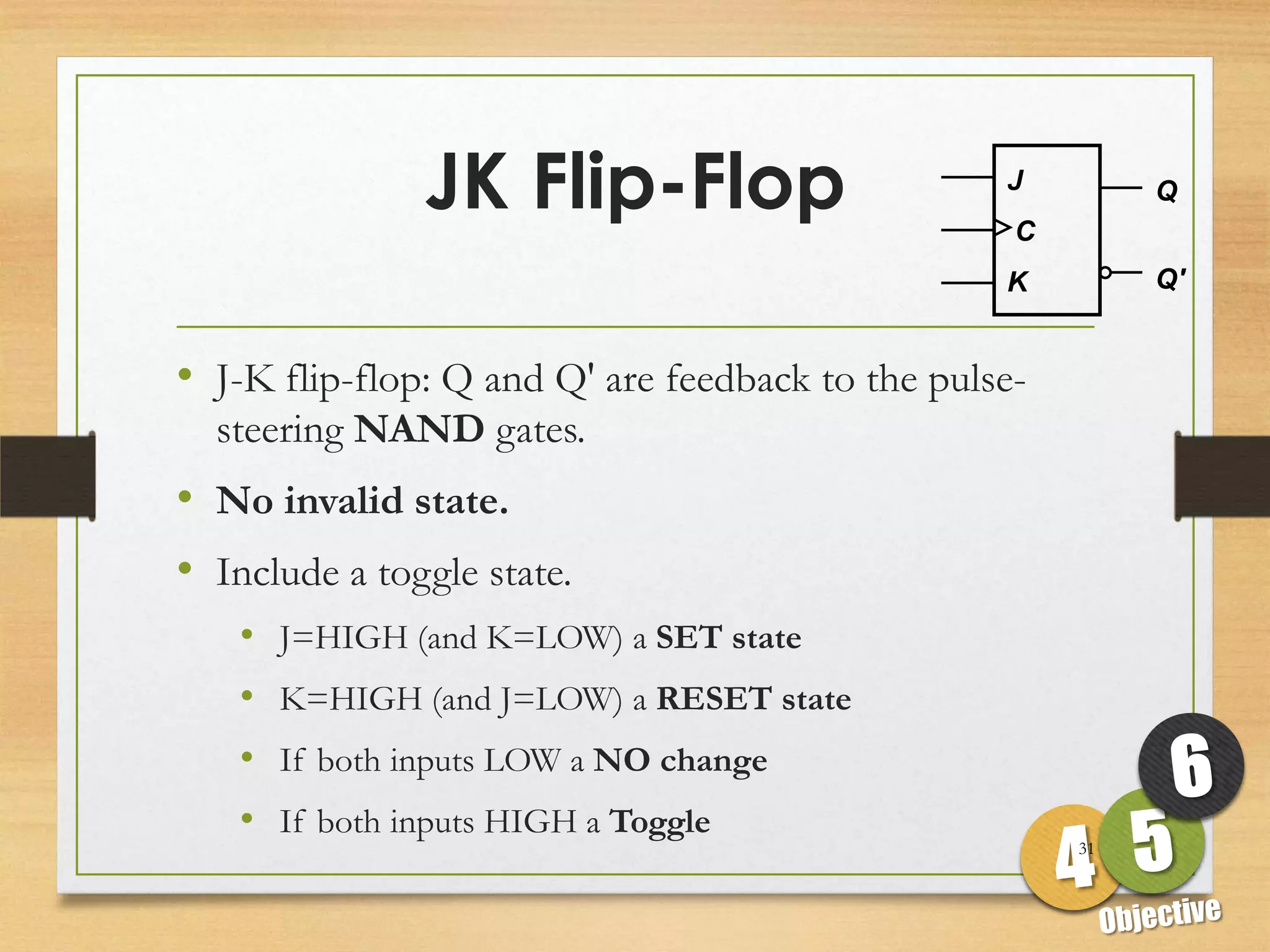
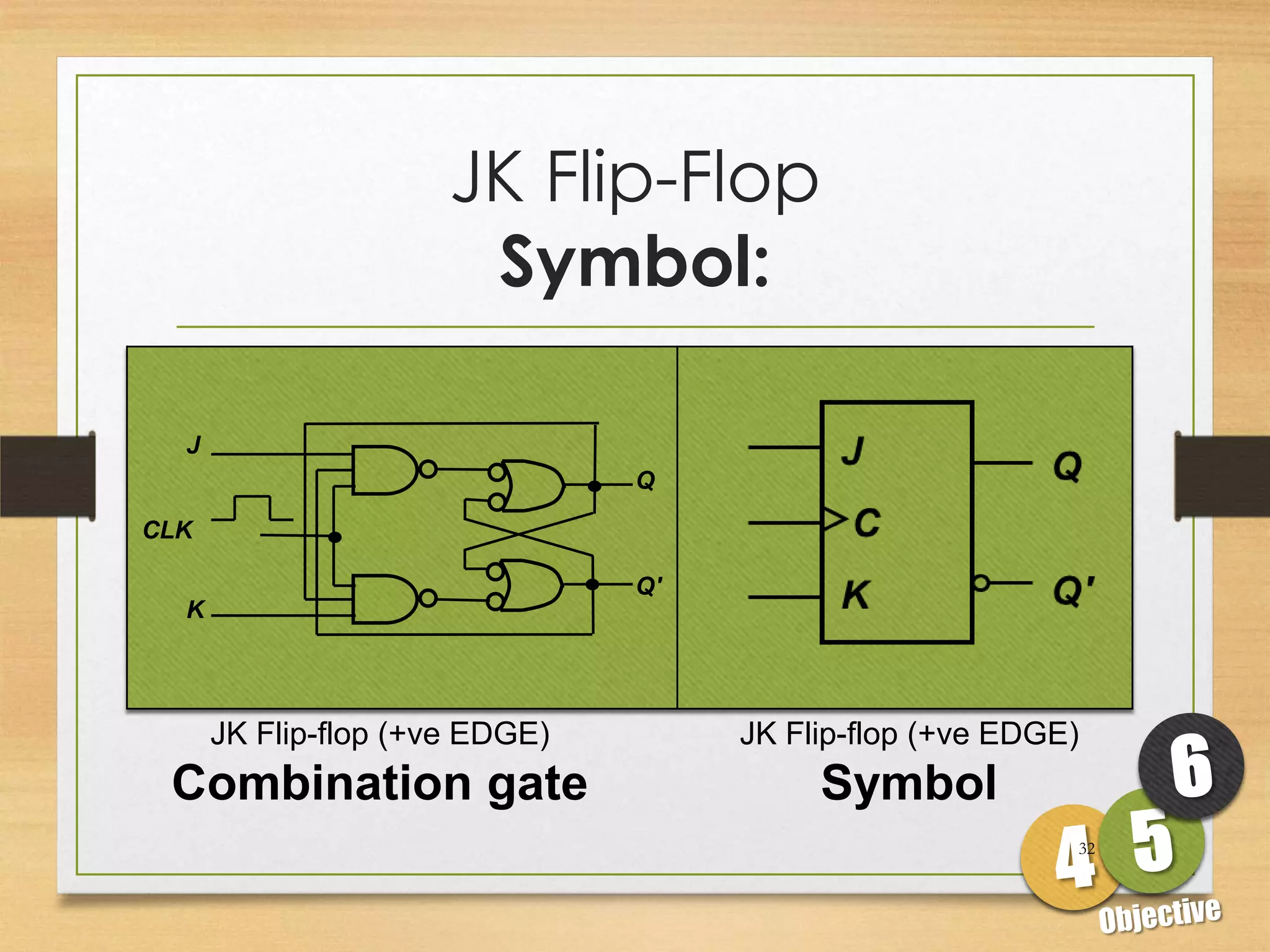
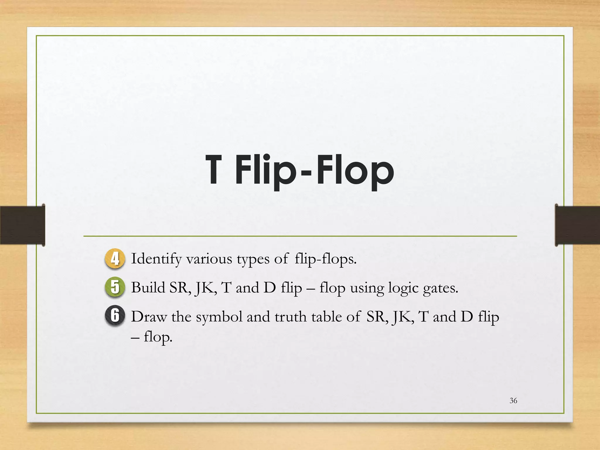
This document discusses sequential logic circuits and flip-flops. It begins by defining sequential logic and differentiating it from combinational logic. It then describes flip-flops as the basic building blocks of sequential logic that provide memory. It identifies four common types of flip-flops - SR, JK, D and T - and describes their operation, truth tables and implementation using logic gates. The document provides details on each type of flip-flop to help understand their functionality and applications in sequential logic circuits.
SEQUENTIAL CIRCUITS [FLIP FLOPS AND LATCHES]SUBHA SHREE
This presentation is about the sequential logic circuits, mainly concentrating on flip-flops and latches. A unique feature in this presentation is the incorporation of circuit images generated from Multisim software imparting practical knowledge to the users. This consists of both the active low and high versions of different circuits.
The document explains about the concepts of sequential circuits in Digital electronics.
This will be helpful for the beginners in VLSI and electronics students.
JK flip flop in Digital electronics
You can watch my lectures at:
Digital electronics playlist in my youtube channel:
https://www.youtube.com/channel/UC_fItK7wBO6zdWHVPIYV8dQ?view_as=subscriber
My Website : https://easyninspire.blogspot.com/
The Reason Why we use master slave JK flip flop instead of simple level triggered flip flop is Racing condition which can be successfully avoided using two SR latches fed with inverted clocks.
Primary Programs Framework - Curriculum Integration: Making ConnectionsSarah Sue Calbio
Alberta Education,. (2007). Primary Programs Framework - Curriculum Integration: Making Connections. Alberta, Canada: Alberta Education. Retrieved from https://education.alberta.ca/media/563581/guidingprinc_curr2007.pdf
in this ppt i have disused about Flip flop with diagram and truth table.. i have explained each types of Flip flop briefly clearly..
computers and calculators use Flip-flop for their memory. A combination of number of flip flops will produce some amount of memory.
Flip flop is formed using logic gates, which are in turn made of transistors. Flip flop are basic building blocks in the memory of electronic devices. Each flip flop can store one bit of data.
SEQUENTIAL LOGIC CIRCUITS (FLIP FLOPS AND LATCHES)Sairam Adithya
this presentation is about the sequential logic circuits, mainly concentrating on flip-flops and latches. a unique feature in this presentation is the incorporation of circuit images generated from Multisim software imparting practical knowledge to the users. this consists of both the active low and high versions of different circuits.
This presentation is about the sequential logic circuits, mainly concentrating on flip-flops and latches. A unique feature in this presentation is the incorporation of circuit images generated from Multisim software imparting practical knowledge to the users.
Rs flipflop or SR flipFLop
You can watch my lectures at:
Digital electronics playlist in my youtube channel:
https://www.youtube.com/channel/UC_fItK7wBO6zdWHVPIYV8dQ?view_as=subscriber
My Website : https://easyninspire.blogspot.com/
A Strategic Approach: GenAI in EducationPeter Windle
Artificial Intelligence (AI) technologies such as Generative AI, Image Generators and Large Language Models have had a dramatic impact on teaching, learning and assessment over the past 18 months. The most immediate threat AI posed was to Academic Integrity with Higher Education Institutes (HEIs) focusing their efforts on combating the use of GenAI in assessment. Guidelines were developed for staff and students, policies put in place too. Innovative educators have forged paths in the use of Generative AI for teaching, learning and assessments leading to pockets of transformation springing up across HEIs, often with little or no top-down guidance, support or direction.
This Gasta posits a strategic approach to integrating AI into HEIs to prepare staff, students and the curriculum for an evolving world and workplace. We will highlight the advantages of working with these technologies beyond the realm of teaching, learning and assessment by considering prompt engineering skills, industry impact, curriculum changes, and the need for staff upskilling. In contrast, not engaging strategically with Generative AI poses risks, including falling behind peers, missed opportunities and failing to ensure our graduates remain employable. The rapid evolution of AI technologies necessitates a proactive and strategic approach if we are to remain relevant.
Model Attribute Check Company Auto PropertyCeline George
In Odoo, the multi-company feature allows you to manage multiple companies within a single Odoo database instance. Each company can have its own configurations while still sharing common resources such as products, customers, and suppliers.
The French Revolution, which began in 1789, was a period of radical social and political upheaval in France. It marked the decline of absolute monarchies, the rise of secular and democratic republics, and the eventual rise of Napoleon Bonaparte. This revolutionary period is crucial in understanding the transition from feudalism to modernity in Europe.
For more information, visit-www.vavaclasses.com
Safalta Digital marketing institute in Noida, provide complete applications that encompass a huge range of virtual advertising and marketing additives, which includes search engine optimization, virtual communication advertising, pay-per-click on marketing, content material advertising, internet analytics, and greater. These university courses are designed for students who possess a comprehensive understanding of virtual marketing strategies and attributes.Safalta Digital Marketing Institute in Noida is a first choice for young individuals or students who are looking to start their careers in the field of digital advertising. The institute gives specialized courses designed and certification.
for beginners, providing thorough training in areas such as SEO, digital communication marketing, and PPC training in Noida. After finishing the program, students receive the certifications recognised by top different universitie, setting a strong foundation for a successful career in digital marketing.
Introduction to AI for Nonprofits with Tapp NetworkTechSoup
Dive into the world of AI! Experts Jon Hill and Tareq Monaur will guide you through AI's role in enhancing nonprofit websites and basic marketing strategies, making it easy to understand and apply.
Synthetic Fiber Construction in lab .pptxPavel ( NSTU)
Synthetic fiber production is a fascinating and complex field that blends chemistry, engineering, and environmental science. By understanding these aspects, students can gain a comprehensive view of synthetic fiber production, its impact on society and the environment, and the potential for future innovations. Synthetic fibers play a crucial role in modern society, impacting various aspects of daily life, industry, and the environment. ynthetic fibers are integral to modern life, offering a range of benefits from cost-effectiveness and versatility to innovative applications and performance characteristics. While they pose environmental challenges, ongoing research and development aim to create more sustainable and eco-friendly alternatives. Understanding the importance of synthetic fibers helps in appreciating their role in the economy, industry, and daily life, while also emphasizing the need for sustainable practices and innovation.
Unit 8 - Information and Communication Technology (Paper I).pdfThiyagu K
This slides describes the basic concepts of ICT, basics of Email, Emerging Technology and Digital Initiatives in Education. This presentations aligns with the UGC Paper I syllabus.
2. Objectives:
•
1 Define sequential logic circuit.
•
2 Differentiate between combinational logic circuit and
sequential logic circuit.
•
3 Describe flip - flop.
•
4 Identify various types of flip-flops.
•
5 Build SR, JK, T and D flip – flop using logic gates.
•
6 Draw the symbol and truth table of SR, JK, T and D flip
– flop.
2
4. Difference between
Combinational & Sequential logic circuit
Combinational Logic Circuits
Basic building
blocks include:
Sequential Logic Circuits
Basic building blocks
include FLIP-FLOPS:
4
5. Sequential S
C
Q
logic circuit R Q'
• Sequential logic is the type of digital system
that does not only depend on current input, but
also the previous history of the system.
• For that reason sequential logic requires
memory elements to function.
• The building blocks used to construct devices
that store data are called flip-flops.
5
6. Sequential logic circuit
Sequential circuit have loops
– these enable curcuits to receive feedback 6
7. Combinational
logic circuit
• Combinational logic is an interconnection of
logic gates to generate a specificities logic
function where the inputs result in an
immediate output, having no memory or
storage capabilities.
• There are function only based on their
inputs, and NOT based on clocks.
7
10. Flip-Flop
• "Flip-flop" is the common name given to two-state
devices which offer basic memory for sequential
logic operations.
• Flip-flops are heavily used for digital data storage and
transfer and are commonly used in banks called
"registers" for the storage of binary numerical
data.
10
11. Flip-Flop
• Flip-flop are basic storage/memory elements.
• Flip-flop are essentially 1-bit storage devices.
• Types of flip-flops are:
• 1. SR Flip-flop
• 2. JK Flip-flop
• 3. D Flip-flop
• 4. T Flip-flop
• Application of flip-flop:
• 1. Counter 4. Logic controller
• 2. Register 5. Frequency Divider
• 3. Memory
11
12. SR Flip-Flop
4 Identify various types of flip-flops.
5 Build SR, JK, T and D flip – flop using logic gates.
6 Draw the symbol and truth table of SR, JK, T and D flip
– flop.
12
13. SR Flip-Flop S Q
R Q'
• The simplest binary storage device.
• SR Flip-flop have 2 inputs (SET & RESET) and 2
outputs (Q & Q’).
NOTE: Q & Q’ are compliments of each other
• The SR flip flop is sometimes referred to as an SR
latch. The Term latch refers to its use as a
temporary memory storage device.
13
14. SR Flip-Flop
Symbol:
SR Flip-flop (Active HIGH) SR Flip-flop (Active HIGH)
NOR gate Symbol
14
15. SR Flip-Flop
Symbol:
SR Flip-flop (Active LOW) SR Flip-flop (Active LOW)
NAND gate Symbol
15
16. SR Flip-Flop
Truth Table:
S R Q Q'
No change. Latch S Q
0 0 NC NC
remained in present state.
1 0 1 0 Latch SET. R Q'
0 1 0 1 Latch RESET.
SR Flip-flop
1 1 0 0 Invalid condition. (Active HIGH)
S' R' Q Q'
No change. Latch S Q
1 1 NC NC
remained in present state.
0 1 1 0 Latch SET. R Q'
1 0 0 1 Latch RESET.
SR Flip-flop
0 0 1 1 Invalid condition.
(Active LOW)
16
18. IQ Test!
What is the mode of operation of the SR flip-flop (set, reset or hold)?
What is the output at Q from the SR flip-flop (active LOW inputs)?
L
?
High
H
Mode of operation = Set
?
H
?
High
H
Mode of operation = Hold
?
H
?
Low
L
Mode of operation = ?
Reset 18
19. Clock
SR Flip-Flop
4 Identify various types of flip-flops.
5 Build SR, JK, T and D flip – flop using logic gates.
6 Draw the symbol and truth table of SR, JK, T and D flip
– flop.
19
20. Clock
• Flip-flops: synchronous bistable devices
• Output changes state at a specified point on a
triggering input called the clock.
• Change state either at the positive edge (rising edge) or
at the negative edge (falling edge) of the clock signal.
Clock signal
Positive Negative edges
edges
20
21. Clock
SR Flip-Flop
• The Clocked SR Flip Flop like SR flip-flop but with
extra third input of a standard clock pulse.
• The output of Q and NOT Q will not change
(despite making changes to the inputs Set & Reset)
in a Clocked RS Flip-flop Until receiving a signal
from the clock.
21
22. Clock SR Flip-Flop
Symbol:
Clock SR Flip-flop (+ve EDGE) Clock SR Flip-flop (+ve EDGE)
Combination gate Symbol
22
24. Clock SR Flip-Flop
Truth Table:
• S-R flip-flop: on the triggering edge of the clock pulse,
• S=HIGH and R=LOW is a SET state
• R=HIGH (and S=LOW) is a RESET state
• If both SR inputs LOW a NO change
• If both SR inputs HIGH a INVALID
• Truth table of positive edge-triggered S-R flip-flop:
S R CLK Q(t+1) Comments
X = irrelevant (“don’t care”)
0 0 X Q(t) No change = clock transition LOW to HIGH
0 1 0 Reset
1 0 1 Set
1 1 ? Invalid
24
25. Clock SR Flip-Flop
Timing Diagram:
How if we add clock as input?
Please draw the output waveform for me
(Positive edge triggered)
25
26. D Flip-Flop
4 Identify various types of flip-flops.
5 Build SR, JK, T and D flip – flop using logic gates.
6 Draw the symbol and truth table of SR, JK, T and D flip
– flop.
26
27. D Flip-Flop D Q
Truth Table:
C
Q'
• D flip-flop: single input D (data)
• D=HIGH a SET state
• D=LOW a RESET state
• Q follows D at the clock edge.
• D flip-flop formed by add NOT gate between SR input.
D S Q D CLK Q(t+1) Comments
CLK C 1 1 Set
R Q' 0 0 Reset
= clock transition LOW to HIGH
27
28. D Flip-Flop
Symbol:
D
Q
CLK
Q'
D Flip-flop (+ve EDGE) D Flip-flop (+ve EDGE)
Combination gate Symbol
28
30. JK Flip-Flop
4 Identify various types of flip-flops.
5 Build SR, JK, T and D flip – flop using logic gates.
6 Draw the symbol and truth table of SR, JK, T and D flip
– flop.
30
31. JK Flip-Flop J
C
Q
K Q'
• J-K flip-flop: Q and Q' are feedback to the pulse-
steering NAND gates.
• No invalid state.
• Include a toggle state.
• J=HIGH (and K=LOW) a SET state
• K=HIGH (and J=LOW) a RESET state
• If both inputs LOW a NO change
• If both inputs HIGH a Toggle
31
32. JK Flip-Flop
Symbol:
J
Q
CLK
Q'
K
JK Flip-flop (+ve EDGE) JK Flip-flop (+ve EDGE)
Combination gate Symbol
32
33. JK Flip-Flop
Truth Table:
J K CLK Q(t+1) Comments
0 0 Q(t) No change
0 1 0 Reset
1 0 1 Set
1 1 Q(t)' Toggle
33
34. JK Flip-Flop
Application: Frequency Division
High High High
J J QA J QB
Q
CLK C CLK C C
K K K
CLK CLK
Q QA
QB
Divide clock frequency by 2. Divide clock frequency by 4.
34
35. JK Flip-Flop
Timing Diagram:
Similar to S-R flip-flop but toggles when J = K = 1
35
36. T Flip-Flop
4 Identify various types of flip-flops.
5 Build SR, JK, T and D flip – flop using logic gates.
6 Draw the symbol and truth table of SR, JK, T and D flip
– flop.
36
37. T Flip-Flop T J Q
Truth Table:
CLK C
K Q'
• T flip-flop: single-input version of the J-K flip
flop, formed by tying both inputs together.
T T CLK Q(t+1) Comments
Q
0 Q(t) No change
CLK 1 Q(t)' Toggle
Q'
37