SlideShare a Scribd company logo
ECE 410, Prof. A. Mason Lecture Notes 13.1
Memory Basics
• RAM: Random Access Memory
– historically defined as memory array with individual bit access
– refers to memory with both Read and Write capabilities
• ROM: Read Only Memory
– no capabilities for “online” memory Write operations
– Write typically requires high voltages or erasing by UV light
• Volatility of Memory
– volatile memory loses data over time or when power is removed
• RAM is volatile
– non-volatile memory stores date even when power is removed
• ROM is non-volatile
• Static vs. Dynamic Memory
– Static: holds data as long as power is applied (SRAM)
– Dynamic: must be refreshed periodically (DRAM)
ECE 410, Prof. A. Mason Lecture Notes 13.2
SRAM Basics
• SRAM = Static Random Access Memory
– Static: holds data as long as power is applied
– Volatile: can not hold data if power is removed
• 3 Operation States
– hold
– write
– read
• Basic 6T (6 transistor) SRAM Cell
– bistable (cross-coupled) INVs for storage
– access transistors MAL & MAR
• access to stored data for read and write
– word line, WL, controls access
• WL = 0, hold operation
• WL = 1, read or write operation
WL
MAR
MAL
bit bit
ECE 410, Prof. A. Mason Lecture Notes 13.3
• Hold
– word line = 0, access transistors are OFF
– data held in latch
• Write
– word line = 1, access tx are ON
– new data (voltage) applied to bit and bit_bar
– data in latch overwritten with new value
• Read
– word line = 1, access tx are ON
– bit and bit_bar read by a sense amplifier
• Sense Amplifier
– basically a simple differential amplifier
– comparing the difference between bit and bit_bar
• if bit > bit_bar, output is 1
• if bit < bit_bar, output is 0
• allows output to be set quickly without fully charging/discharging bit line
SRAM Operations
WL=0
MAR
MAL
bit bit
WL=1
MAR
MAL
bit bit
ECE 410, Prof. A. Mason Lecture Notes 13.4
SRAM Bit Cell Circuit
• Two SRAM cells dominate CMOS industry
– 6T Cell
• all CMOS transistors
• better noise immunity
– 4T Cell
• replaces pMOS with high resistance (~1GΩ) resistors
• slightly smaller than 6T cell
• requires an extra high-resistance process layer
ECE 410, Prof. A. Mason Lecture Notes 13.5
6T Cell Design
• Critical Design Challenge
– inverter sizing
• to ensure good hold and easy/fast overwrite
– use minimum sized transistors to save area
• unless more robust design required
• Write Operation
– both bit and bit_bar applied
• inputs to inverters both change
• unlike DFF where one INV overrides the other
– critical size ratio, βA/βn
• see resistor model
– want Rn & Rp larger than RA
» so voltage will drop across Rn, Rp
• typical value, βA/βn=2
– so Rn = 2 RA
– set by ratio (W/L)A to (W/L)n
Resistor Model
Write 1 Operation
ECE 410, Prof. A. Mason Lecture Notes 13.6
SRAM Cell Layout
• Design Challenge
– minimum cell size (for high density SRAM array)
– with good access to word and bit lines
• Example Layout
– note WL routed in poly
• will create a large RC delay
for large SRAM array
ECE 410, Prof. A. Mason Lecture Notes 13.7
Multi-Port SRAM
• Allows multiple access to the same SRAM cell simultaneously.
– Provide high data bandwidth.
• Applications
– Register file
– Cache
– Network switch
– ASIC etc.
D2
D1
D1
D2
Ws1
Ws2
• A multi-port SRAM cell
schematic. Each port has
– two access transistors
– two bit line
– one word selection line.
– one address decoder
inverter feedback loop
bit access bit_bar
access
ECE 410, Prof. A. Mason Lecture Notes 13.8
Multi-Port SRAM (cont.)
• Challenges in multi-ports SRAM.
– layout size increases quadratically with # of ports
• more word selection lines
• more bitline lines
– Æ lower speed and higher power consumption
• Multi-port SRAM options for ECE410 Design Project
– Two ports
• 1 port read and write
• 1 port read only
– Three ports
• 2 ports for read and 1 port for write
ECE 410, Prof. A. Mason Lecture Notes 13.9
SRAM Arrays
• N x n array of 1-bit cells
– n = byte width; 8, 16, 32, etc.
– N = number of bytes
– m = number of address bits
• max N = 2m
• Array I/O
– data, in and out
• Dn-1 - D0
– address
• Am-1 - A0
– control
• varies with design
• WE = write enable (assert low)
– WE=1=read, WE=0=write
• En = block enable (assert low)
– used as chip enable (CE) for an SRAM chip
Data I/O
Control
Address
ECE 410, Prof. A. Mason Lecture Notes 13.10
SRAM Block Architecture
• Example: 2-Core design
– core width = k•n
• n = SRAM word size; 8, 16, etc.
• k = multiplier factor, 2,3,4,etc.
– shared word-line circuits
• horizontal word lines
• WL set by row decoder
– placed in center of 2 cores
– WL in both cores selected at same time
• Addressing Operation
– address word determines which row is
active (which WL =1) via row decoder
– row decoder outputs feed row drivers
• buffers to drive large WL capacitance
• Physical Design
– layout scheme matches regular
patterning shown in schematic
• horizontal and vertical routing
Expanded Core View
Basic SRAM
Block Architecture
ECE 410, Prof. A. Mason Lecture Notes 13.11
SRAM Array Addressing
• Standard SRAM Addressing Scheme
– consider a N x n SRAM array
• N = number of bytes, e.g., 512, 2k
• n = byte size, e.g., 8 or 16
– m address bits are divided into x row bits and y column bits (x+y=m)
• address bits are encoded so that 2m = N
• array organized with both both vertical and horizontal stacks of bytes
Rows
Columns
1 SRAM byte
ECE 410, Prof. A. Mason Lecture Notes 13.12
SRAM Array Addressing
• Address Latch
– D-latch with enable and output buffers
– outputs both A and A_bar
• Address Bits
– Row address bits = Word Lines, WL
– Column address bits select a subset of bits activated by WL
• Column Organization
– typically, organized physically by bits, not by bytes
– Example, SRAM with 4-bit bytes in 3 columns (y=3)
• 3 4-bit bytes in each row
Byte 1
Byte 2
Byte 3
D3 D2 D1 D0
y0
y1
y2
Column
Address
Address Latch
(Row) Word Line 1 SRAM bit
4th bits 1’s bits
3rd bits 2nd bits
vertical bit lines
bit_bar not shown
ECE 410, Prof. A. Mason Lecture Notes 13.13
SRAM Array Column Circuits
• SRAM Row Driver
– decoder output, Dec_out
– enable, En, after address bits decoded
• Row Decoder/Driver activate a row of cells
– each 2-core row contains 2k bytes (2k•n bits)
• Column Multiplexers
– address signals select one of the k bytes as final output
not used in row decoder
– figure shows example for k=3
• for an 8-bit RAM (word size)
– MUX used for Read operations
– De MUX used for Write op.s
• Column Drivers
– bit/bit_bar output for Write operations
size-scaled buffers
Row Driver Circuit
Column MUX/DeMUXs
Column
Driver Circuit
pull-
ups
ECE 410, Prof. A. Mason Lecture Notes 13.14
Column Circuitry
• Precharge Concept
– common to use dynamic circuits in SRAMS
• dynamic circuits have precharge and evaluate phases
– precharge high capacitance on bit lines
• avoids heavy capacitive loading on each SRAM cell
• Precharge Phase
– all bit lines pulled to VDD
– all bit_bar to ground
• Evaluate Phase
– bits activated by WL connect to bit lines
• if data = 1, keep precharged value
• if data = 0, discharge bit line Data In Data Out
ECE 410, Prof. A. Mason Lecture Notes 13.15
Bit line (column) Circuitry
• expanded (transistor-level) view of SRAM column
pMOS precharge loads
- charge when φ = 0
nMOS switches select
which column/bit is
passed to Read/Write circuit
word lines
(row address)
column
address
ECE 410, Prof. A. Mason Lecture Notes 13.16
Sense Amplifiers
• Read sensing scheme
– look at differential signal
• bit and bit_bar
– can get output before bit lines
fully charge/discharge by
amplifying differential signals
• Differential Amplifier
– simple analog circuit
– output high
• if bit > bit_bar
– output low
• if bit_bar > bit
– can implement as dynamic circuit
Differential
Amplifier
ECE 410, Prof. A. Mason Lecture Notes 13.17
DRAM Basics
• DRAM = Dynamic Random Access Memory
– Dynamic: must be refreshed periodically
– Volatile: loses data when power is removed
• Comparison to SRAM
– DRAM is smaller & less expensive per bit
– SRAM is faster
– DRAM requires more peripheral circuitry
• 1T DRAM Cell
– single access nFET
– storage capacitor (referenced to VDD or Ground)
– control input: word line, WL
– data I/O: bit line
ECE 410, Prof. A. Mason Lecture Notes 13.18
DRAM Operation
• RAM data is held on the storage capacitor
– temporary –due to leakage currents which drain charge
• Charge Storage
– if Cs is charged to Vs
– Qs = Cs Vs
• if Vs = 0, then Qs = 0: LOGIC 0
• if Vs = large, then Qs > 0: LOGIC 1
• Write Operation
– turn on access transistor: WL = VDD
– apply voltage, Vd (high or low), to bit line
– Cs is charged (or discharged)
– if Vd = 0
• Vs = 0, Qs = 0, store logic 0
– if Vd = VDD
• Vs = VDD-Vtn, Qs = Cs(VDD=Vtn), logic 1
• Hold Operation
– turn off access transistor: WL = 0
• charge held on Cs
ECE 410, Prof. A. Mason Lecture Notes 13.19
Hold Time
• During Hold, leakage currents will slowly discharge Cs
– due to leakage in the access transistor when it is OFF
– IL = -δQs/δt = -Cs δVs/δt
• if IL is known, can determine discharge time
• Hold Time, th
– max time voltage on Cs is high enough to be a logic 1
• = time to discharge from Vmax to V1 (in figure above)
– th = (Cs/IL)(ΔVs), if we estimate IL as a constant
• desire large hold time
• th increases with larger Cs and lower IL
• typical value, th = 50μsec
– with IL = 1nA, Cs=50fF, and ΔVs=1V
error in textbook, says 0.5μsec near Eqn. 13.
0.1
1
10
100
1000
10000
100000
1000000
0.0001 0.001 0.01 0.1 1 10 100
leakage current (nA)
hold
time
(usec)
ECE 410, Prof. A. Mason Lecture Notes 13.20
Refresh Rate
• DRAM is “Dynamic”, data is stored for only short time
• Refresh Operation
– to hold data as long as power is applied, data must be refreshed
– periodically read every cell
• amplify cell data
• rewrite data to cell
• Refresh Rate, frefresh
– frequency at which cells must be
refreshed to maintain data
– frefresh = 1 / 2th
– must include refresh circuitry
in a DRAM circuit
Refresh operation
ECE 410, Prof. A. Mason Lecture Notes 13.21
DRAM Read Operation
• Read Operation
– turn on access transistor
– charge on Cs is redistributed on the bit line capacitance, Cbit
– this will change the bit line voltage, Vbit
– which is amplified to read a 1 or 0
• Charge Redistribution
– initial charge on Cs: Qs = Cs Vs
– redistributed on Cbit until
• Vbit = Vs = Vf (final voltage)
– Qs = Cs Vf + Cbit Vf
– Cs Vs = Vf (Cs + Cbit)
• due to charge conservation
– Vf = Cs Vs / (Cs + Cbit), which is always less than Vs
• Vf typically very small and requires a good sense amplifier
ECE 410, Prof. A. Mason Lecture Notes 13.22
DRAM Read Operation (cont.)
• DRAM Read Operation is Destructive
– charge redistribution destroys the stored
information
– read operation must contain a simultaneous
rewrite
• Sense Amplifier
– SA_En is the enable for the sense
amplifier
– when EQ is high both sides of the sense
amp are shorted together. The circuit then
holds at it’s midpoint voltage creating a
precharge.
– the input and output of the sense amp
share the same node which allows for a
simultaneous rewrite
http://jas.eng.buffalo.edu/education/system/senseamp/
ECE 410, Prof. A. Mason Lecture Notes 13.23
DRAM Physical Design
• Physical design (layout) is CRITICAL in DRAM
– high density is required for commercial success
– current technology provides > 1Gb on a DRAM chip
• Must minimize area of the 1T DRAM cell
– typically only 30% of the chip is needed for peripherals (refresh, etc.)
• For DRAM in CMOS, must minimize area of storage capacitor
– but, large capacitor (> 40fF) is good to increase hold time, th
• Storage Capacitor Examples
– trench capacitor
• junction cap. with large junction area
• using etched pit
– stacked capacitor
• cap. on top of access tx
• using poly plate capacitor
ECE 410, Prof. A. Mason Lecture Notes 13.24
ROM Basics
• ROM: Read Only Memory
– no capabilities for “online” memory Write operations
– data programmed
• during fabrication: ROM
• with high voltages: PROM
• by control logic: PLA
– Non-volatile: data stored even when power is removed
• NOR-based ROM
– Example: 8b words stored by NOR-based ROM
– address selects an active ‘row’
– each output bit connected
to the active row will be
high
– otherwise, output will be low
ECE 410, Prof. A. Mason Lecture Notes 13.25
Pseudo-nMOS ROM
• Pseudo-nMOS
– always ON active pMOS load
• pulls output high if nMOS is off
– controlled nMOS switch
• pulls output low if input is high
• competes with pMOS
– must be sized properly
• consumes power when output is low
• ROM Structure
– address is decoded to
choose and active ‘row’
– each row line turns on
nMOS where output is zero
– otherwise, output stays high
• Set ROM Data
– by selectively connecting
nMOS to the output lines
pMOS pull-ups outputs
nMOS pull-downs
ECE 410, Prof. A. Mason Lecture Notes 13.26
ROM Arrays
• Pseudo nMOS Arrays
– most common style for large ROMS
• Design Concerns
– nMOS must “overdrive” pMOS
– need βn > βp so that VOL is low enough
• must set Wn > Wp
• but, this also increases
row line capacitance
– requires careful analog design
• Programming Methods
– mask programmable
• create nMOS at all points
• define data with poly contacts
– layout programmable
• only place nMOS where needed
• shown in figure Æ
ECE 410, Prof. A. Mason Lecture Notes 13.27
ROM Array Layout
• very “regular” layout
• high packing density
– one tx for each
data point
ECE 410, Prof. A. Mason Lecture Notes 13.28
Programmable ROM
• PROM
– programmable by user
• using special program tools/modes
– read only memory
• during normal use
– non-volatile
• Read Operation
– like any ROM: address bits select output bit combinations
• Write Operation
– typically requires high voltage (~15V) control inputs to set data
• Erase Operation
– to change data
– EPROM: erasable PROM: uses UV light to reset all bits
– EEPROM: electrically-erasable PROM, erase with control voltage
ECE 410, Prof. A. Mason Lecture Notes 13.29
PROM Storage Cells
• Physical Structure
– pair of stacked poly gates
• top gate acts as normal access/control gate
• bottom gate is ‘floating’, changes threshold voltage
• Cell Operation
– no charge on floating gate
• transistor has normal Vtn
– negative charge on floating gate
• opposes action of applied gate voltage
• keeps transistor turned off
– unless a high VtnH is applied; VtnH > VDD so will not turn on with normal voltages
ECE 410, Prof. A. Mason Lecture Notes 13.30
EPROM Arrays
• Structure is similar to a RAM Array
• WL selects which word of data will connect to output
• When WL is high
– each tx in the selected data byte will set the output bit line
• if floating gate has no charge, bit line will pull down for a LOGIC 0
• if floating gate is charged, tx will not turn on and bit line will remain
high for a LOGIC 1
• Column circuitry can be used to form arrays, as in RAM
one word in an 8b-wide EPROM
ECE 410, Prof. A. Mason Lecture Notes 13.31
Programming & Erasing E2PROMs
• Programming techniques
– hot electron method
• charge (electrons) transferred to the floating
gate by quantum mechanical tunneling of hot
electrons (high energy electrons)
• accomplished by applying a high voltage (~12-30V)
to the drain node
• charge can remain on floating gate for 10-20 years!
– Fowler-Nordheim emission
• uses modified gate geometry to allow quantum
mechanical tunneling from the drain into the
floating gate
• Erasure Techniques
– bit erasure: by reversing programming voltages
– flash EPROMs: erase large block simultaneously
ECE 410, Prof. A. Mason Lecture Notes 13.32
Programmable Logic Arrays
• Programmable Logic Array: PLA
– circuit which can be programmed to provide various logic
functions
• Example: Sum-of-Products PLA
– with four inputs (a, b, c, d), the possible SOP outputs are
• f = Σ mi(a,b,c,d) [OR minterms]
• where mi(a,b,c,d) are the minterms [AND inputs]
– has an AND-OR structure which
can be reproduced in circuits
ECE 410, Prof. A. Mason Lecture Notes 13.33
AND-OR PLA Implementation
• Logic Array Diagram
– example for
• fx = m0 + m4 + m5
• fy = m3 + m4 + m5 + m15
• etc.
• Programming PLA
– transistor switch at each
optional connection location
– turn tx on to make connection
• VLSI Implementation
– replace AND-OR with NOR gates
15
error in text
ECE 410, Prof. A. Mason Lecture Notes 13.34
Gate Arrays
• Gate array chip contains
– a huge array of logic gates
– programmable connections
• allows gates to be combined to make larger functions (e.g., DFF)
• Field Programmable Gate Array (FGPA)
– connections can be programmed easily to redefine function
– can have more than 100,000 logic gates on an FPGA
• capable of emulating complex functions, like a 32-bit microprocessor
– program techniques: the antifuse concept
• physical design: built-in fuses where connections might be wanted
• high current short-circuits the fuse to create low resistance path

More Related Content

What's hot

FPGA
FPGAFPGA
RF Module Design - [Chapter 3] Linearity
RF Module Design - [Chapter 3]  LinearityRF Module Design - [Chapter 3]  Linearity
RF Module Design - [Chapter 3] Linearity
Simen Li
 
AVR ATmega32
AVR ATmega32AVR ATmega32
AVR ATmega32
Prashant Tiwari
 
Fan-in and Fan-out.ppt
Fan-in and Fan-out.pptFan-in and Fan-out.ppt
Fan-in and Fan-out.ppt
vsnishok
 
Design of cmos based ring oscillator
Design of cmos based ring oscillatorDesign of cmos based ring oscillator
Design of cmos based ring oscillator
Ushaswini Chowdary
 
VLSI Technology Trends
VLSI Technology TrendsVLSI Technology Trends
VLSI Technology Trends
Usha Mehta
 
Physical Verification Design.pdf
Physical Verification Design.pdfPhysical Verification Design.pdf
Physical Verification Design.pdf
Ahmed Abdelazeem
 
UNIT I- CPLD & FPGA ARCHITECTURE & APPLICATIONS
UNIT I- CPLD & FPGA ARCHITECTURE & APPLICATIONSUNIT I- CPLD & FPGA ARCHITECTURE & APPLICATIONS
UNIT I- CPLD & FPGA ARCHITECTURE & APPLICATIONS
Dr.YNM
 
Code conversion using verilog code VHDL
Code conversion using verilog code VHDL Code conversion using verilog code VHDL
Code conversion using verilog code VHDL
Bharti Airtel Ltd.
 
Rc delay modelling in vlsi
Rc delay modelling in vlsiRc delay modelling in vlsi
Rc delay modelling in vlsi
Dr. Vishal Sharma
 
optimazation of standard cell layout
optimazation of standard cell layoutoptimazation of standard cell layout
optimazation of standard cell layout
E ER Yash nagaria
 
SoC: System On Chip
SoC: System On ChipSoC: System On Chip
SoC: System On Chip
Santosh Verma
 
CMOS Logic Circuits
CMOS Logic CircuitsCMOS Logic Circuits
CMOS Logic Circuits
Marmik Kothari
 
Design And Analysis of Charge Pump for PLL at 90nm CMOS technology
Design And Analysis of Charge Pump for PLL at 90nm CMOS technologyDesign And Analysis of Charge Pump for PLL at 90nm CMOS technology
Design And Analysis of Charge Pump for PLL at 90nm CMOS technology
Ravi Chandra
 
Sequential cmos logic circuits
Sequential cmos logic circuitsSequential cmos logic circuits
Sequential cmos logic circuits
Sakshi Bhargava
 
SoC Design
SoC DesignSoC Design
Fpga architectures and applications
Fpga architectures and applicationsFpga architectures and applications
Fpga architectures and applications
Sudhanshu Janwadkar
 
Session 2,3 FPGAs
Session 2,3 FPGAsSession 2,3 FPGAs
Session 2,3 FPGAs
Subhash Iyer
 
Combinational circuit (7-Segment display)
Combinational circuit (7-Segment display)Combinational circuit (7-Segment display)
Combinational circuit (7-Segment display)
ali9753
 
System partitioning in VLSI and its considerations
System partitioning in VLSI and its considerationsSystem partitioning in VLSI and its considerations
System partitioning in VLSI and its considerations
Subash John
 

What's hot (20)

FPGA
FPGAFPGA
FPGA
 
RF Module Design - [Chapter 3] Linearity
RF Module Design - [Chapter 3]  LinearityRF Module Design - [Chapter 3]  Linearity
RF Module Design - [Chapter 3] Linearity
 
AVR ATmega32
AVR ATmega32AVR ATmega32
AVR ATmega32
 
Fan-in and Fan-out.ppt
Fan-in and Fan-out.pptFan-in and Fan-out.ppt
Fan-in and Fan-out.ppt
 
Design of cmos based ring oscillator
Design of cmos based ring oscillatorDesign of cmos based ring oscillator
Design of cmos based ring oscillator
 
VLSI Technology Trends
VLSI Technology TrendsVLSI Technology Trends
VLSI Technology Trends
 
Physical Verification Design.pdf
Physical Verification Design.pdfPhysical Verification Design.pdf
Physical Verification Design.pdf
 
UNIT I- CPLD & FPGA ARCHITECTURE & APPLICATIONS
UNIT I- CPLD & FPGA ARCHITECTURE & APPLICATIONSUNIT I- CPLD & FPGA ARCHITECTURE & APPLICATIONS
UNIT I- CPLD & FPGA ARCHITECTURE & APPLICATIONS
 
Code conversion using verilog code VHDL
Code conversion using verilog code VHDL Code conversion using verilog code VHDL
Code conversion using verilog code VHDL
 
Rc delay modelling in vlsi
Rc delay modelling in vlsiRc delay modelling in vlsi
Rc delay modelling in vlsi
 
optimazation of standard cell layout
optimazation of standard cell layoutoptimazation of standard cell layout
optimazation of standard cell layout
 
SoC: System On Chip
SoC: System On ChipSoC: System On Chip
SoC: System On Chip
 
CMOS Logic Circuits
CMOS Logic CircuitsCMOS Logic Circuits
CMOS Logic Circuits
 
Design And Analysis of Charge Pump for PLL at 90nm CMOS technology
Design And Analysis of Charge Pump for PLL at 90nm CMOS technologyDesign And Analysis of Charge Pump for PLL at 90nm CMOS technology
Design And Analysis of Charge Pump for PLL at 90nm CMOS technology
 
Sequential cmos logic circuits
Sequential cmos logic circuitsSequential cmos logic circuits
Sequential cmos logic circuits
 
SoC Design
SoC DesignSoC Design
SoC Design
 
Fpga architectures and applications
Fpga architectures and applicationsFpga architectures and applications
Fpga architectures and applications
 
Session 2,3 FPGAs
Session 2,3 FPGAsSession 2,3 FPGAs
Session 2,3 FPGAs
 
Combinational circuit (7-Segment display)
Combinational circuit (7-Segment display)Combinational circuit (7-Segment display)
Combinational circuit (7-Segment display)
 
System partitioning in VLSI and its considerations
System partitioning in VLSI and its considerationsSystem partitioning in VLSI and its considerations
System partitioning in VLSI and its considerations
 

Similar to Ch13.pdf

Computer Organisation and Architecture
Computer Organisation and ArchitectureComputer Organisation and Architecture
Computer Organisation and Architecture
Subhasis Dash
 
Lec11 Computer Architecture by Hsien-Hsin Sean Lee Georgia Tech -- Memory part3
Lec11 Computer Architecture by Hsien-Hsin Sean Lee Georgia Tech -- Memory part3Lec11 Computer Architecture by Hsien-Hsin Sean Lee Georgia Tech -- Memory part3
Lec11 Computer Architecture by Hsien-Hsin Sean Lee Georgia Tech -- Memory part3
Hsien-Hsin Sean Lee, Ph.D.
 
DLC logic families and memory
DLC logic families and memoryDLC logic families and memory
DLC logic families and memory
balu prithviraj
 
sramanddram.ppt
sramanddram.pptsramanddram.ppt
sramanddram.ppt
AmalNath44
 
DRAM Cell - Working and Read and Write Operations
DRAM Cell - Working and Read and Write OperationsDRAM Cell - Working and Read and Write Operations
DRAM Cell - Working and Read and Write Operations
Naman Bhalla
 
Unit- 4 Computer Oganization and Architecture
Unit- 4 Computer Oganization and ArchitectureUnit- 4 Computer Oganization and Architecture
Unit- 4 Computer Oganization and Architecture
thangamsuresh3
 
Computer organization memory
Computer organization memoryComputer organization memory
Computer organization memory
Deepak John
 
SRAM read and write and sense amplifier
SRAM read and write and sense amplifierSRAM read and write and sense amplifier
SRAM read and write and sense amplifier
Soumyajit Langal
 
Readonly memories DMAcontrollerand .pptx
Readonly memories DMAcontrollerand .pptxReadonly memories DMAcontrollerand .pptx
Readonly memories DMAcontrollerand .pptx
sirishaYerraboina1
 
Random Access Memory
Random Access Memory Random Access Memory
Random Access Memory
rohitladdu
 
Unit IV Memory.pptx
Unit IV  Memory.pptxUnit IV  Memory.pptx
Unit IV Memory.pptx
madhukarvnimbalkar
 
Sram pdf
Sram pdfSram pdf
Microelectronics U4.pptx.ppt
Microelectronics U4.pptx.pptMicroelectronics U4.pptx.ppt
Microelectronics U4.pptx.ppt
PavikaSharma3
 
Memory Hierarchy PPT of Computer Organization
Memory Hierarchy PPT of Computer OrganizationMemory Hierarchy PPT of Computer Organization
Memory Hierarchy PPT of Computer Organization
2022002857mbit
 
SRAM DRAM
SRAM DRAMSRAM DRAM
SRAM DRAM
Tipu Sultan
 
lect13.ppt
lect13.pptlect13.ppt
lect13.ppt
shoaib574322
 
memory system notes.pptx
memory system notes.pptxmemory system notes.pptx
memory system notes.pptx
1DA21CS173
 
Static and Dynamic Read/Write memories
Static and Dynamic Read/Write memoriesStatic and Dynamic Read/Write memories
Static and Dynamic Read/Write memories
Abhilash Nair
 
SRAM
SRAMSRAM
Chapter5 the memory-system-jntuworld
Chapter5 the memory-system-jntuworldChapter5 the memory-system-jntuworld
Chapter5 the memory-system-jntuworld
Praveen Kumar
 

Similar to Ch13.pdf (20)

Computer Organisation and Architecture
Computer Organisation and ArchitectureComputer Organisation and Architecture
Computer Organisation and Architecture
 
Lec11 Computer Architecture by Hsien-Hsin Sean Lee Georgia Tech -- Memory part3
Lec11 Computer Architecture by Hsien-Hsin Sean Lee Georgia Tech -- Memory part3Lec11 Computer Architecture by Hsien-Hsin Sean Lee Georgia Tech -- Memory part3
Lec11 Computer Architecture by Hsien-Hsin Sean Lee Georgia Tech -- Memory part3
 
DLC logic families and memory
DLC logic families and memoryDLC logic families and memory
DLC logic families and memory
 
sramanddram.ppt
sramanddram.pptsramanddram.ppt
sramanddram.ppt
 
DRAM Cell - Working and Read and Write Operations
DRAM Cell - Working and Read and Write OperationsDRAM Cell - Working and Read and Write Operations
DRAM Cell - Working and Read and Write Operations
 
Unit- 4 Computer Oganization and Architecture
Unit- 4 Computer Oganization and ArchitectureUnit- 4 Computer Oganization and Architecture
Unit- 4 Computer Oganization and Architecture
 
Computer organization memory
Computer organization memoryComputer organization memory
Computer organization memory
 
SRAM read and write and sense amplifier
SRAM read and write and sense amplifierSRAM read and write and sense amplifier
SRAM read and write and sense amplifier
 
Readonly memories DMAcontrollerand .pptx
Readonly memories DMAcontrollerand .pptxReadonly memories DMAcontrollerand .pptx
Readonly memories DMAcontrollerand .pptx
 
Random Access Memory
Random Access Memory Random Access Memory
Random Access Memory
 
Unit IV Memory.pptx
Unit IV  Memory.pptxUnit IV  Memory.pptx
Unit IV Memory.pptx
 
Sram pdf
Sram pdfSram pdf
Sram pdf
 
Microelectronics U4.pptx.ppt
Microelectronics U4.pptx.pptMicroelectronics U4.pptx.ppt
Microelectronics U4.pptx.ppt
 
Memory Hierarchy PPT of Computer Organization
Memory Hierarchy PPT of Computer OrganizationMemory Hierarchy PPT of Computer Organization
Memory Hierarchy PPT of Computer Organization
 
SRAM DRAM
SRAM DRAMSRAM DRAM
SRAM DRAM
 
lect13.ppt
lect13.pptlect13.ppt
lect13.ppt
 
memory system notes.pptx
memory system notes.pptxmemory system notes.pptx
memory system notes.pptx
 
Static and Dynamic Read/Write memories
Static and Dynamic Read/Write memoriesStatic and Dynamic Read/Write memories
Static and Dynamic Read/Write memories
 
SRAM
SRAMSRAM
SRAM
 
Chapter5 the memory-system-jntuworld
Chapter5 the memory-system-jntuworldChapter5 the memory-system-jntuworld
Chapter5 the memory-system-jntuworld
 

Recently uploaded

CHINA’S GEO-ECONOMIC OUTREACH IN CENTRAL ASIAN COUNTRIES AND FUTURE PROSPECT
CHINA’S GEO-ECONOMIC OUTREACH IN CENTRAL ASIAN COUNTRIES AND FUTURE PROSPECTCHINA’S GEO-ECONOMIC OUTREACH IN CENTRAL ASIAN COUNTRIES AND FUTURE PROSPECT
CHINA’S GEO-ECONOMIC OUTREACH IN CENTRAL ASIAN COUNTRIES AND FUTURE PROSPECT
jpsjournal1
 
CSM Cloud Service Management Presentarion
CSM Cloud Service Management PresentarionCSM Cloud Service Management Presentarion
CSM Cloud Service Management Presentarion
rpskprasana
 
22CYT12-Unit-V-E Waste and its Management.ppt
22CYT12-Unit-V-E Waste and its Management.ppt22CYT12-Unit-V-E Waste and its Management.ppt
22CYT12-Unit-V-E Waste and its Management.ppt
KrishnaveniKrishnara1
 
官方认证美国密歇根州立大学毕业证学位证书原版一模一样
官方认证美国密歇根州立大学毕业证学位证书原版一模一样官方认证美国密歇根州立大学毕业证学位证书原版一模一样
官方认证美国密歇根州立大学毕业证学位证书原版一模一样
171ticu
 
basic-wireline-operations-course-mahmoud-f-radwan.pdf
basic-wireline-operations-course-mahmoud-f-radwan.pdfbasic-wireline-operations-course-mahmoud-f-radwan.pdf
basic-wireline-operations-course-mahmoud-f-radwan.pdf
NidhalKahouli2
 
Advanced control scheme of doubly fed induction generator for wind turbine us...
Advanced control scheme of doubly fed induction generator for wind turbine us...Advanced control scheme of doubly fed induction generator for wind turbine us...
Advanced control scheme of doubly fed induction generator for wind turbine us...
IJECEIAES
 
Literature Review Basics and Understanding Reference Management.pptx
Literature Review Basics and Understanding Reference Management.pptxLiterature Review Basics and Understanding Reference Management.pptx
Literature Review Basics and Understanding Reference Management.pptx
Dr Ramhari Poudyal
 
Question paper of renewable energy sources
Question paper of renewable energy sourcesQuestion paper of renewable energy sources
Question paper of renewable energy sources
mahammadsalmanmech
 
Embedded machine learning-based road conditions and driving behavior monitoring
Embedded machine learning-based road conditions and driving behavior monitoringEmbedded machine learning-based road conditions and driving behavior monitoring
Embedded machine learning-based road conditions and driving behavior monitoring
IJECEIAES
 
132/33KV substation case study Presentation
132/33KV substation case study Presentation132/33KV substation case study Presentation
132/33KV substation case study Presentation
kandramariana6
 
Heat Resistant Concrete Presentation ppt
Heat Resistant Concrete Presentation pptHeat Resistant Concrete Presentation ppt
Heat Resistant Concrete Presentation ppt
mamunhossenbd75
 
Harnessing WebAssembly for Real-time Stateless Streaming Pipelines
Harnessing WebAssembly for Real-time Stateless Streaming PipelinesHarnessing WebAssembly for Real-time Stateless Streaming Pipelines
Harnessing WebAssembly for Real-time Stateless Streaming Pipelines
Christina Lin
 
Engineering Drawings Lecture Detail Drawings 2014.pdf
Engineering Drawings Lecture Detail Drawings 2014.pdfEngineering Drawings Lecture Detail Drawings 2014.pdf
Engineering Drawings Lecture Detail Drawings 2014.pdf
abbyasa1014
 
DEEP LEARNING FOR SMART GRID INTRUSION DETECTION: A HYBRID CNN-LSTM-BASED MODEL
DEEP LEARNING FOR SMART GRID INTRUSION DETECTION: A HYBRID CNN-LSTM-BASED MODELDEEP LEARNING FOR SMART GRID INTRUSION DETECTION: A HYBRID CNN-LSTM-BASED MODEL
DEEP LEARNING FOR SMART GRID INTRUSION DETECTION: A HYBRID CNN-LSTM-BASED MODEL
gerogepatton
 
ML Based Model for NIDS MSc Updated Presentation.v2.pptx
ML Based Model for NIDS MSc Updated Presentation.v2.pptxML Based Model for NIDS MSc Updated Presentation.v2.pptx
ML Based Model for NIDS MSc Updated Presentation.v2.pptx
JamalHussainArman
 
Modelagem de um CSTR com reação endotermica.pdf
Modelagem de um CSTR com reação endotermica.pdfModelagem de um CSTR com reação endotermica.pdf
Modelagem de um CSTR com reação endotermica.pdf
camseq
 
Presentation of IEEE Slovenia CIS (Computational Intelligence Society) Chapte...
Presentation of IEEE Slovenia CIS (Computational Intelligence Society) Chapte...Presentation of IEEE Slovenia CIS (Computational Intelligence Society) Chapte...
Presentation of IEEE Slovenia CIS (Computational Intelligence Society) Chapte...
University of Maribor
 
Eric Nizeyimana's document 2006 from gicumbi to ttc nyamata handball play
Eric Nizeyimana's document 2006 from gicumbi to ttc nyamata handball playEric Nizeyimana's document 2006 from gicumbi to ttc nyamata handball play
Eric Nizeyimana's document 2006 from gicumbi to ttc nyamata handball play
enizeyimana36
 
Iron and Steel Technology Roadmap - Towards more sustainable steelmaking.pdf
Iron and Steel Technology Roadmap - Towards more sustainable steelmaking.pdfIron and Steel Technology Roadmap - Towards more sustainable steelmaking.pdf
Iron and Steel Technology Roadmap - Towards more sustainable steelmaking.pdf
RadiNasr
 
Textile Chemical Processing and Dyeing.pdf
Textile Chemical Processing and Dyeing.pdfTextile Chemical Processing and Dyeing.pdf
Textile Chemical Processing and Dyeing.pdf
NazakatAliKhoso2
 

Recently uploaded (20)

CHINA’S GEO-ECONOMIC OUTREACH IN CENTRAL ASIAN COUNTRIES AND FUTURE PROSPECT
CHINA’S GEO-ECONOMIC OUTREACH IN CENTRAL ASIAN COUNTRIES AND FUTURE PROSPECTCHINA’S GEO-ECONOMIC OUTREACH IN CENTRAL ASIAN COUNTRIES AND FUTURE PROSPECT
CHINA’S GEO-ECONOMIC OUTREACH IN CENTRAL ASIAN COUNTRIES AND FUTURE PROSPECT
 
CSM Cloud Service Management Presentarion
CSM Cloud Service Management PresentarionCSM Cloud Service Management Presentarion
CSM Cloud Service Management Presentarion
 
22CYT12-Unit-V-E Waste and its Management.ppt
22CYT12-Unit-V-E Waste and its Management.ppt22CYT12-Unit-V-E Waste and its Management.ppt
22CYT12-Unit-V-E Waste and its Management.ppt
 
官方认证美国密歇根州立大学毕业证学位证书原版一模一样
官方认证美国密歇根州立大学毕业证学位证书原版一模一样官方认证美国密歇根州立大学毕业证学位证书原版一模一样
官方认证美国密歇根州立大学毕业证学位证书原版一模一样
 
basic-wireline-operations-course-mahmoud-f-radwan.pdf
basic-wireline-operations-course-mahmoud-f-radwan.pdfbasic-wireline-operations-course-mahmoud-f-radwan.pdf
basic-wireline-operations-course-mahmoud-f-radwan.pdf
 
Advanced control scheme of doubly fed induction generator for wind turbine us...
Advanced control scheme of doubly fed induction generator for wind turbine us...Advanced control scheme of doubly fed induction generator for wind turbine us...
Advanced control scheme of doubly fed induction generator for wind turbine us...
 
Literature Review Basics and Understanding Reference Management.pptx
Literature Review Basics and Understanding Reference Management.pptxLiterature Review Basics and Understanding Reference Management.pptx
Literature Review Basics and Understanding Reference Management.pptx
 
Question paper of renewable energy sources
Question paper of renewable energy sourcesQuestion paper of renewable energy sources
Question paper of renewable energy sources
 
Embedded machine learning-based road conditions and driving behavior monitoring
Embedded machine learning-based road conditions and driving behavior monitoringEmbedded machine learning-based road conditions and driving behavior monitoring
Embedded machine learning-based road conditions and driving behavior monitoring
 
132/33KV substation case study Presentation
132/33KV substation case study Presentation132/33KV substation case study Presentation
132/33KV substation case study Presentation
 
Heat Resistant Concrete Presentation ppt
Heat Resistant Concrete Presentation pptHeat Resistant Concrete Presentation ppt
Heat Resistant Concrete Presentation ppt
 
Harnessing WebAssembly for Real-time Stateless Streaming Pipelines
Harnessing WebAssembly for Real-time Stateless Streaming PipelinesHarnessing WebAssembly for Real-time Stateless Streaming Pipelines
Harnessing WebAssembly for Real-time Stateless Streaming Pipelines
 
Engineering Drawings Lecture Detail Drawings 2014.pdf
Engineering Drawings Lecture Detail Drawings 2014.pdfEngineering Drawings Lecture Detail Drawings 2014.pdf
Engineering Drawings Lecture Detail Drawings 2014.pdf
 
DEEP LEARNING FOR SMART GRID INTRUSION DETECTION: A HYBRID CNN-LSTM-BASED MODEL
DEEP LEARNING FOR SMART GRID INTRUSION DETECTION: A HYBRID CNN-LSTM-BASED MODELDEEP LEARNING FOR SMART GRID INTRUSION DETECTION: A HYBRID CNN-LSTM-BASED MODEL
DEEP LEARNING FOR SMART GRID INTRUSION DETECTION: A HYBRID CNN-LSTM-BASED MODEL
 
ML Based Model for NIDS MSc Updated Presentation.v2.pptx
ML Based Model for NIDS MSc Updated Presentation.v2.pptxML Based Model for NIDS MSc Updated Presentation.v2.pptx
ML Based Model for NIDS MSc Updated Presentation.v2.pptx
 
Modelagem de um CSTR com reação endotermica.pdf
Modelagem de um CSTR com reação endotermica.pdfModelagem de um CSTR com reação endotermica.pdf
Modelagem de um CSTR com reação endotermica.pdf
 
Presentation of IEEE Slovenia CIS (Computational Intelligence Society) Chapte...
Presentation of IEEE Slovenia CIS (Computational Intelligence Society) Chapte...Presentation of IEEE Slovenia CIS (Computational Intelligence Society) Chapte...
Presentation of IEEE Slovenia CIS (Computational Intelligence Society) Chapte...
 
Eric Nizeyimana's document 2006 from gicumbi to ttc nyamata handball play
Eric Nizeyimana's document 2006 from gicumbi to ttc nyamata handball playEric Nizeyimana's document 2006 from gicumbi to ttc nyamata handball play
Eric Nizeyimana's document 2006 from gicumbi to ttc nyamata handball play
 
Iron and Steel Technology Roadmap - Towards more sustainable steelmaking.pdf
Iron and Steel Technology Roadmap - Towards more sustainable steelmaking.pdfIron and Steel Technology Roadmap - Towards more sustainable steelmaking.pdf
Iron and Steel Technology Roadmap - Towards more sustainable steelmaking.pdf
 
Textile Chemical Processing and Dyeing.pdf
Textile Chemical Processing and Dyeing.pdfTextile Chemical Processing and Dyeing.pdf
Textile Chemical Processing and Dyeing.pdf
 

Ch13.pdf

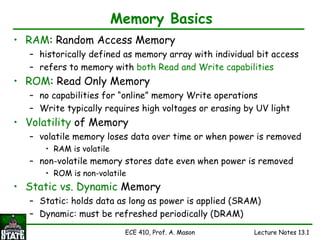
  • 1. ECE 410, Prof. A. Mason Lecture Notes 13.1 Memory Basics • RAM: Random Access Memory – historically defined as memory array with individual bit access – refers to memory with both Read and Write capabilities • ROM: Read Only Memory – no capabilities for “online” memory Write operations – Write typically requires high voltages or erasing by UV light • Volatility of Memory – volatile memory loses data over time or when power is removed • RAM is volatile – non-volatile memory stores date even when power is removed • ROM is non-volatile • Static vs. Dynamic Memory – Static: holds data as long as power is applied (SRAM) – Dynamic: must be refreshed periodically (DRAM)
  • 2. ECE 410, Prof. A. Mason Lecture Notes 13.2 SRAM Basics • SRAM = Static Random Access Memory – Static: holds data as long as power is applied – Volatile: can not hold data if power is removed • 3 Operation States – hold – write – read • Basic 6T (6 transistor) SRAM Cell – bistable (cross-coupled) INVs for storage – access transistors MAL & MAR • access to stored data for read and write – word line, WL, controls access • WL = 0, hold operation • WL = 1, read or write operation WL MAR MAL bit bit
  • 3. ECE 410, Prof. A. Mason Lecture Notes 13.3 • Hold – word line = 0, access transistors are OFF – data held in latch • Write – word line = 1, access tx are ON – new data (voltage) applied to bit and bit_bar – data in latch overwritten with new value • Read – word line = 1, access tx are ON – bit and bit_bar read by a sense amplifier • Sense Amplifier – basically a simple differential amplifier – comparing the difference between bit and bit_bar • if bit > bit_bar, output is 1 • if bit < bit_bar, output is 0 • allows output to be set quickly without fully charging/discharging bit line SRAM Operations WL=0 MAR MAL bit bit WL=1 MAR MAL bit bit
  • 4. ECE 410, Prof. A. Mason Lecture Notes 13.4 SRAM Bit Cell Circuit • Two SRAM cells dominate CMOS industry – 6T Cell • all CMOS transistors • better noise immunity – 4T Cell • replaces pMOS with high resistance (~1GΩ) resistors • slightly smaller than 6T cell • requires an extra high-resistance process layer
  • 5. ECE 410, Prof. A. Mason Lecture Notes 13.5 6T Cell Design • Critical Design Challenge – inverter sizing • to ensure good hold and easy/fast overwrite – use minimum sized transistors to save area • unless more robust design required • Write Operation – both bit and bit_bar applied • inputs to inverters both change • unlike DFF where one INV overrides the other – critical size ratio, βA/βn • see resistor model – want Rn & Rp larger than RA » so voltage will drop across Rn, Rp • typical value, βA/βn=2 – so Rn = 2 RA – set by ratio (W/L)A to (W/L)n Resistor Model Write 1 Operation
  • 6. ECE 410, Prof. A. Mason Lecture Notes 13.6 SRAM Cell Layout • Design Challenge – minimum cell size (for high density SRAM array) – with good access to word and bit lines • Example Layout – note WL routed in poly • will create a large RC delay for large SRAM array
  • 7. ECE 410, Prof. A. Mason Lecture Notes 13.7 Multi-Port SRAM • Allows multiple access to the same SRAM cell simultaneously. – Provide high data bandwidth. • Applications – Register file – Cache – Network switch – ASIC etc. D2 D1 D1 D2 Ws1 Ws2 • A multi-port SRAM cell schematic. Each port has – two access transistors – two bit line – one word selection line. – one address decoder inverter feedback loop bit access bit_bar access
  • 8. ECE 410, Prof. A. Mason Lecture Notes 13.8 Multi-Port SRAM (cont.) • Challenges in multi-ports SRAM. – layout size increases quadratically with # of ports • more word selection lines • more bitline lines – Æ lower speed and higher power consumption • Multi-port SRAM options for ECE410 Design Project – Two ports • 1 port read and write • 1 port read only – Three ports • 2 ports for read and 1 port for write
  • 9. ECE 410, Prof. A. Mason Lecture Notes 13.9 SRAM Arrays • N x n array of 1-bit cells – n = byte width; 8, 16, 32, etc. – N = number of bytes – m = number of address bits • max N = 2m • Array I/O – data, in and out • Dn-1 - D0 – address • Am-1 - A0 – control • varies with design • WE = write enable (assert low) – WE=1=read, WE=0=write • En = block enable (assert low) – used as chip enable (CE) for an SRAM chip Data I/O Control Address
  • 10. ECE 410, Prof. A. Mason Lecture Notes 13.10 SRAM Block Architecture • Example: 2-Core design – core width = k•n • n = SRAM word size; 8, 16, etc. • k = multiplier factor, 2,3,4,etc. – shared word-line circuits • horizontal word lines • WL set by row decoder – placed in center of 2 cores – WL in both cores selected at same time • Addressing Operation – address word determines which row is active (which WL =1) via row decoder – row decoder outputs feed row drivers • buffers to drive large WL capacitance • Physical Design – layout scheme matches regular patterning shown in schematic • horizontal and vertical routing Expanded Core View Basic SRAM Block Architecture
  • 11. ECE 410, Prof. A. Mason Lecture Notes 13.11 SRAM Array Addressing • Standard SRAM Addressing Scheme – consider a N x n SRAM array • N = number of bytes, e.g., 512, 2k • n = byte size, e.g., 8 or 16 – m address bits are divided into x row bits and y column bits (x+y=m) • address bits are encoded so that 2m = N • array organized with both both vertical and horizontal stacks of bytes Rows Columns 1 SRAM byte
  • 12. ECE 410, Prof. A. Mason Lecture Notes 13.12 SRAM Array Addressing • Address Latch – D-latch with enable and output buffers – outputs both A and A_bar • Address Bits – Row address bits = Word Lines, WL – Column address bits select a subset of bits activated by WL • Column Organization – typically, organized physically by bits, not by bytes – Example, SRAM with 4-bit bytes in 3 columns (y=3) • 3 4-bit bytes in each row Byte 1 Byte 2 Byte 3 D3 D2 D1 D0 y0 y1 y2 Column Address Address Latch (Row) Word Line 1 SRAM bit 4th bits 1’s bits 3rd bits 2nd bits vertical bit lines bit_bar not shown
  • 13. ECE 410, Prof. A. Mason Lecture Notes 13.13 SRAM Array Column Circuits • SRAM Row Driver – decoder output, Dec_out – enable, En, after address bits decoded • Row Decoder/Driver activate a row of cells – each 2-core row contains 2k bytes (2k•n bits) • Column Multiplexers – address signals select one of the k bytes as final output not used in row decoder – figure shows example for k=3 • for an 8-bit RAM (word size) – MUX used for Read operations – De MUX used for Write op.s • Column Drivers – bit/bit_bar output for Write operations size-scaled buffers Row Driver Circuit Column MUX/DeMUXs Column Driver Circuit pull- ups
  • 14. ECE 410, Prof. A. Mason Lecture Notes 13.14 Column Circuitry • Precharge Concept – common to use dynamic circuits in SRAMS • dynamic circuits have precharge and evaluate phases – precharge high capacitance on bit lines • avoids heavy capacitive loading on each SRAM cell • Precharge Phase – all bit lines pulled to VDD – all bit_bar to ground • Evaluate Phase – bits activated by WL connect to bit lines • if data = 1, keep precharged value • if data = 0, discharge bit line Data In Data Out
  • 15. ECE 410, Prof. A. Mason Lecture Notes 13.15 Bit line (column) Circuitry • expanded (transistor-level) view of SRAM column pMOS precharge loads - charge when φ = 0 nMOS switches select which column/bit is passed to Read/Write circuit word lines (row address) column address
  • 16. ECE 410, Prof. A. Mason Lecture Notes 13.16 Sense Amplifiers • Read sensing scheme – look at differential signal • bit and bit_bar – can get output before bit lines fully charge/discharge by amplifying differential signals • Differential Amplifier – simple analog circuit – output high • if bit > bit_bar – output low • if bit_bar > bit – can implement as dynamic circuit Differential Amplifier
  • 17. ECE 410, Prof. A. Mason Lecture Notes 13.17 DRAM Basics • DRAM = Dynamic Random Access Memory – Dynamic: must be refreshed periodically – Volatile: loses data when power is removed • Comparison to SRAM – DRAM is smaller & less expensive per bit – SRAM is faster – DRAM requires more peripheral circuitry • 1T DRAM Cell – single access nFET – storage capacitor (referenced to VDD or Ground) – control input: word line, WL – data I/O: bit line
  • 18. ECE 410, Prof. A. Mason Lecture Notes 13.18 DRAM Operation • RAM data is held on the storage capacitor – temporary –due to leakage currents which drain charge • Charge Storage – if Cs is charged to Vs – Qs = Cs Vs • if Vs = 0, then Qs = 0: LOGIC 0 • if Vs = large, then Qs > 0: LOGIC 1 • Write Operation – turn on access transistor: WL = VDD – apply voltage, Vd (high or low), to bit line – Cs is charged (or discharged) – if Vd = 0 • Vs = 0, Qs = 0, store logic 0 – if Vd = VDD • Vs = VDD-Vtn, Qs = Cs(VDD=Vtn), logic 1 • Hold Operation – turn off access transistor: WL = 0 • charge held on Cs
  • 19. ECE 410, Prof. A. Mason Lecture Notes 13.19 Hold Time • During Hold, leakage currents will slowly discharge Cs – due to leakage in the access transistor when it is OFF – IL = -δQs/δt = -Cs δVs/δt • if IL is known, can determine discharge time • Hold Time, th – max time voltage on Cs is high enough to be a logic 1 • = time to discharge from Vmax to V1 (in figure above) – th = (Cs/IL)(ΔVs), if we estimate IL as a constant • desire large hold time • th increases with larger Cs and lower IL • typical value, th = 50μsec – with IL = 1nA, Cs=50fF, and ΔVs=1V error in textbook, says 0.5μsec near Eqn. 13. 0.1 1 10 100 1000 10000 100000 1000000 0.0001 0.001 0.01 0.1 1 10 100 leakage current (nA) hold time (usec)
  • 20. ECE 410, Prof. A. Mason Lecture Notes 13.20 Refresh Rate • DRAM is “Dynamic”, data is stored for only short time • Refresh Operation – to hold data as long as power is applied, data must be refreshed – periodically read every cell • amplify cell data • rewrite data to cell • Refresh Rate, frefresh – frequency at which cells must be refreshed to maintain data – frefresh = 1 / 2th – must include refresh circuitry in a DRAM circuit Refresh operation
  • 21. ECE 410, Prof. A. Mason Lecture Notes 13.21 DRAM Read Operation • Read Operation – turn on access transistor – charge on Cs is redistributed on the bit line capacitance, Cbit – this will change the bit line voltage, Vbit – which is amplified to read a 1 or 0 • Charge Redistribution – initial charge on Cs: Qs = Cs Vs – redistributed on Cbit until • Vbit = Vs = Vf (final voltage) – Qs = Cs Vf + Cbit Vf – Cs Vs = Vf (Cs + Cbit) • due to charge conservation – Vf = Cs Vs / (Cs + Cbit), which is always less than Vs • Vf typically very small and requires a good sense amplifier
  • 22. ECE 410, Prof. A. Mason Lecture Notes 13.22 DRAM Read Operation (cont.) • DRAM Read Operation is Destructive – charge redistribution destroys the stored information – read operation must contain a simultaneous rewrite • Sense Amplifier – SA_En is the enable for the sense amplifier – when EQ is high both sides of the sense amp are shorted together. The circuit then holds at it’s midpoint voltage creating a precharge. – the input and output of the sense amp share the same node which allows for a simultaneous rewrite http://jas.eng.buffalo.edu/education/system/senseamp/
  • 23. ECE 410, Prof. A. Mason Lecture Notes 13.23 DRAM Physical Design • Physical design (layout) is CRITICAL in DRAM – high density is required for commercial success – current technology provides > 1Gb on a DRAM chip • Must minimize area of the 1T DRAM cell – typically only 30% of the chip is needed for peripherals (refresh, etc.) • For DRAM in CMOS, must minimize area of storage capacitor – but, large capacitor (> 40fF) is good to increase hold time, th • Storage Capacitor Examples – trench capacitor • junction cap. with large junction area • using etched pit – stacked capacitor • cap. on top of access tx • using poly plate capacitor
  • 24. ECE 410, Prof. A. Mason Lecture Notes 13.24 ROM Basics • ROM: Read Only Memory – no capabilities for “online” memory Write operations – data programmed • during fabrication: ROM • with high voltages: PROM • by control logic: PLA – Non-volatile: data stored even when power is removed • NOR-based ROM – Example: 8b words stored by NOR-based ROM – address selects an active ‘row’ – each output bit connected to the active row will be high – otherwise, output will be low
  • 25. ECE 410, Prof. A. Mason Lecture Notes 13.25 Pseudo-nMOS ROM • Pseudo-nMOS – always ON active pMOS load • pulls output high if nMOS is off – controlled nMOS switch • pulls output low if input is high • competes with pMOS – must be sized properly • consumes power when output is low • ROM Structure – address is decoded to choose and active ‘row’ – each row line turns on nMOS where output is zero – otherwise, output stays high • Set ROM Data – by selectively connecting nMOS to the output lines pMOS pull-ups outputs nMOS pull-downs
  • 26. ECE 410, Prof. A. Mason Lecture Notes 13.26 ROM Arrays • Pseudo nMOS Arrays – most common style for large ROMS • Design Concerns – nMOS must “overdrive” pMOS – need βn > βp so that VOL is low enough • must set Wn > Wp • but, this also increases row line capacitance – requires careful analog design • Programming Methods – mask programmable • create nMOS at all points • define data with poly contacts – layout programmable • only place nMOS where needed • shown in figure Æ
  • 27. ECE 410, Prof. A. Mason Lecture Notes 13.27 ROM Array Layout • very “regular” layout • high packing density – one tx for each data point
  • 28. ECE 410, Prof. A. Mason Lecture Notes 13.28 Programmable ROM • PROM – programmable by user • using special program tools/modes – read only memory • during normal use – non-volatile • Read Operation – like any ROM: address bits select output bit combinations • Write Operation – typically requires high voltage (~15V) control inputs to set data • Erase Operation – to change data – EPROM: erasable PROM: uses UV light to reset all bits – EEPROM: electrically-erasable PROM, erase with control voltage
  • 29. ECE 410, Prof. A. Mason Lecture Notes 13.29 PROM Storage Cells • Physical Structure – pair of stacked poly gates • top gate acts as normal access/control gate • bottom gate is ‘floating’, changes threshold voltage • Cell Operation – no charge on floating gate • transistor has normal Vtn – negative charge on floating gate • opposes action of applied gate voltage • keeps transistor turned off – unless a high VtnH is applied; VtnH > VDD so will not turn on with normal voltages
  • 30. ECE 410, Prof. A. Mason Lecture Notes 13.30 EPROM Arrays • Structure is similar to a RAM Array • WL selects which word of data will connect to output • When WL is high – each tx in the selected data byte will set the output bit line • if floating gate has no charge, bit line will pull down for a LOGIC 0 • if floating gate is charged, tx will not turn on and bit line will remain high for a LOGIC 1 • Column circuitry can be used to form arrays, as in RAM one word in an 8b-wide EPROM
  • 31. ECE 410, Prof. A. Mason Lecture Notes 13.31 Programming & Erasing E2PROMs • Programming techniques – hot electron method • charge (electrons) transferred to the floating gate by quantum mechanical tunneling of hot electrons (high energy electrons) • accomplished by applying a high voltage (~12-30V) to the drain node • charge can remain on floating gate for 10-20 years! – Fowler-Nordheim emission • uses modified gate geometry to allow quantum mechanical tunneling from the drain into the floating gate • Erasure Techniques – bit erasure: by reversing programming voltages – flash EPROMs: erase large block simultaneously
  • 32. ECE 410, Prof. A. Mason Lecture Notes 13.32 Programmable Logic Arrays • Programmable Logic Array: PLA – circuit which can be programmed to provide various logic functions • Example: Sum-of-Products PLA – with four inputs (a, b, c, d), the possible SOP outputs are • f = Σ mi(a,b,c,d) [OR minterms] • where mi(a,b,c,d) are the minterms [AND inputs] – has an AND-OR structure which can be reproduced in circuits
  • 33. ECE 410, Prof. A. Mason Lecture Notes 13.33 AND-OR PLA Implementation • Logic Array Diagram – example for • fx = m0 + m4 + m5 • fy = m3 + m4 + m5 + m15 • etc. • Programming PLA – transistor switch at each optional connection location – turn tx on to make connection • VLSI Implementation – replace AND-OR with NOR gates 15 error in text
  • 34. ECE 410, Prof. A. Mason Lecture Notes 13.34 Gate Arrays • Gate array chip contains – a huge array of logic gates – programmable connections • allows gates to be combined to make larger functions (e.g., DFF) • Field Programmable Gate Array (FGPA) – connections can be programmed easily to redefine function – can have more than 100,000 logic gates on an FPGA • capable of emulating complex functions, like a 32-bit microprocessor – program techniques: the antifuse concept • physical design: built-in fuses where connections might be wanted • high current short-circuits the fuse to create low resistance path