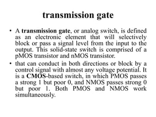
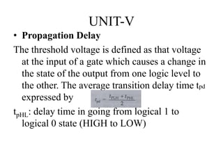
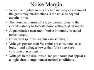
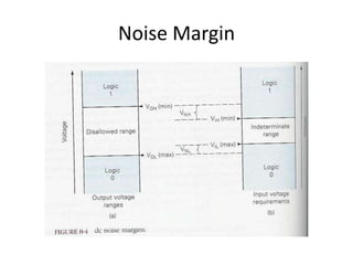
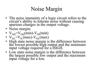
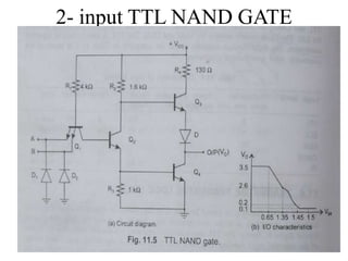
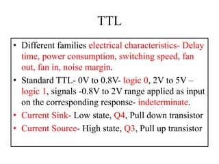
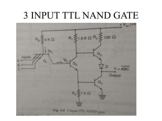
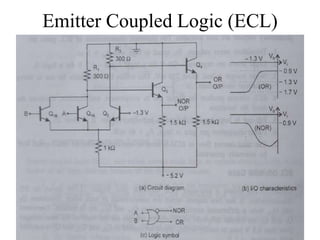
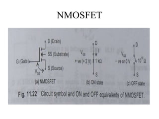
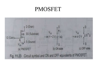
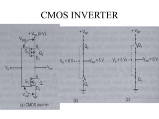
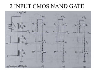
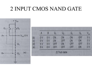
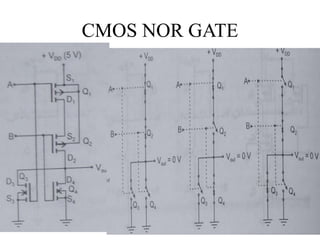
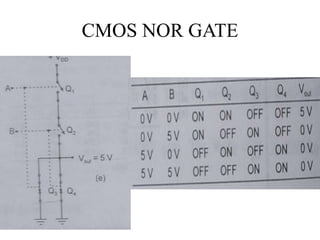
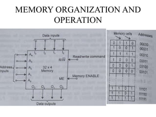
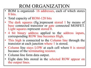
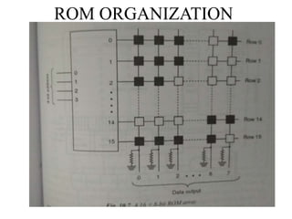
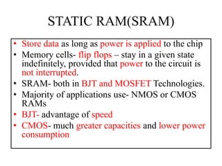
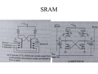
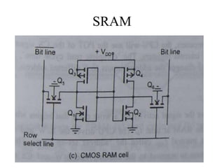
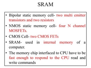
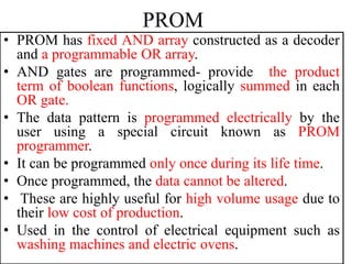
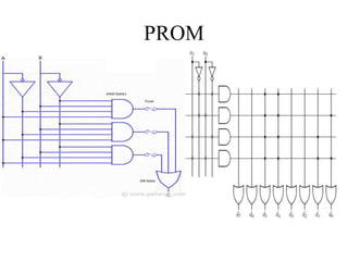
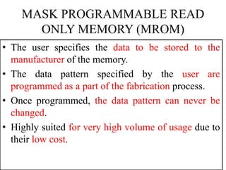
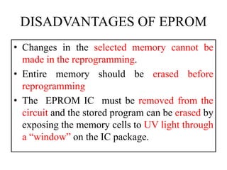
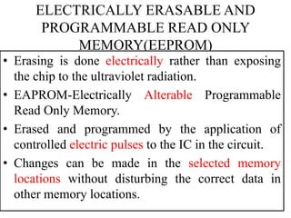
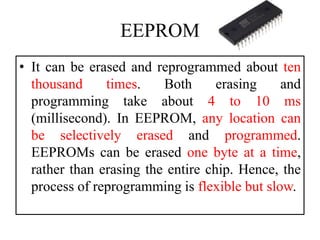
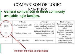
The document discusses various logic families and memory concepts. It provides details on propagation delay, noise margin, TTL NAND gate, ECL logic family characteristics, MOS transistor advantages, CMOS inverter and NAND gate structure, SRAM and DRAM organization and operation, and comparisons between different types of ROM such as PROM, EPROM, and EEPROM.
This document provides an overview of memory types and logic families. It discusses static and dynamic memories, including SRAM and DRAM. Circuit diagrams are presented to illustrate one-bit and larger memory designs. Flash memory and its operation are also covered. The history of transistors, FETs, and integrated circuits is reviewed. Memory timing diagrams and the evolution of programmable logic devices are summarized as well.
The document discusses a 5T SRAM cell for embedded cache memory. It begins by explaining the basic operations of memory and different types of memory like RAM and ROM. It then discusses the structure and operation of a typical 6T SRAM cell. It introduces a 5T SRAM cell that aims to reduce leakage and increase density compared to 6T cells. The document outlines the read and write operations of the 5T cell and provides results of implementing the cell showing improvements in leakage and area. It concludes by discussing potential applications and areas for future work.
This document summarizes a student project to design a 32KB SRAM memory array using Cadence Virtuoso and a 45nm technology. It includes the design of a 6 transistor SRAM cell, row and column decoders, critical path components like the precharge circuit and sense amplifiers. Two types of sense amplifiers - differential and latched-based were modeled and their read delay, power consumption and sizing were compared through simulation. The results showed that the latched-based sense amplifier consumed 14x less power, had less read delay and size making it a better choice compared to the differential sense amplifier.
This document discusses digital logic concepts including binary logic, logic gates, logic families, and programmable logic devices. It defines binary logic as consisting of binary variables and logical operations. It states that the three basic logic gates are AND, OR, and NOT. It also discusses combinational logic circuits, including half adders, full adders, decoders, encoders, multiplexers and comparators. Finally, it covers programmable logic devices such as ROM, PROM, EPROM and EEPROM.
This document provides an overview of the design of a dual port SRAM using Verilog HDL. It begins with an introduction describing the objectives and accomplishments of the project. It then reviews relevant literature on SRAM design. The document describes the FPGA design flow and introduces Verilog. It provides the design and operation of the SRAM, and discusses simulation results and conclusions. The proposed 8-bit dual port SRAM utilizes negative bitline techniques during write operations to improve write ability and reduce power consumption and area compared to conventional designs.
Designed a fully customized 128x10b SRAM by constructing schematic & virtuoso layout of memory cell array (6T cell), row & column decoder, pre-charge circuit, write circuit and sense amplifier using Cadence. Manually placed and routed all components, performed DRC & LVS debugging of constructed schematic and layout and ran PEX to generate the final Netlist, Hspice Spectre simulation of final design for verification of the correct functionality and analysis of best read, best write cycles & the worst case timing for read and write. Timing and power consumed is analyzed through STA-Primetime (Static timing Analysis)
The document describes a proposed novel 8T SRAM cell for ultra-low voltage applications. It begins with an objective to design an 8T SRAM cell that can operate at ultra-low voltages while maintaining low power consumption and improved write and read margins compared to a conventional 6T SRAM cell. It then analyzes the performance of the proposed 8T cell, finding it can operate reliably down to 335mV, with a hold static noise margin of 130mV. The 8T cell exhibits improved write and read stability compared to a 6T cell at ultra-low voltages. In conclusion, the 8T cell design meets the goals of enabling ultra-low voltage operation while improving performance.
Implementation of High Reliable 6T SRAM Cell Designiosrjce
Memory can be formed with the integration of large number of basic storing element called cells.
SRAM cell is one of the basic storing unit of volatile semiconductor memory that stores binary logic '1' or '0' bit.
Modified read and write circuits were proposed in this paper to address incorrect read and write operations in
conventional 6T SRAM cell design available in open literature. Design of a new highly reliable 6T SRAM cell
design is proposed with reliable read, write operations and negative bit line voltage (NBLV). Simulations are
carried out using MENTOR GRAPHICS
In the project#1, IBM 130nm process is used to design and manual layout a 128 word SRAM, with word size 10bits. Cadence's Virtuoso is applied for layout editing, DRC and LVS running and circuit simulation.
This lecture discusses advanced SRAM technologies including FinFET-based SRAM issues and alternatives. It begins with fundamentals of 6T SRAM design and reviews state-of-the-art SRAM performance. Key challenges for FinFET-based SRAM include variability impacts and design tradeoffs. The lecture explores techniques to improve SRAM stability for FinFETs and reviews Intel's 22nm tri-gate SRAM technology. Finally, it discusses SRAM alternatives such as 8T cells, SDRAM, and context memory to address scaling challenges.
A Simplied Bit-Line Technique for Memory Optimizationijsrd.com
High fan-in and fan-out in read-write of memory requires more area, power, and causes large propagation delay .The number of transistor counts also increases due to large fan-in and fan-out. A simplified bit line technique for power optimization of memory proposed consumes steady power, requires less number of transistors and hence reduces the propagation delay for any fan-in and fan-out of read-write memory. Adopting simplified bit line technique, we implemented 32-word 16-bits/word, 32-word 16-bits/word and so on, 1-read, 1-write ported register files in a 1.2-V/2.5V. By using this technique 2n word x m-bits/words can be achieved with steady power consumption of 2.4mW for 1.2V/2.5V, this power consumption can be further reduced to half of present level by constraining the parameters such as temperature, speed, frequency of operation etc for processing technology.
This document summarizes different types of computer memory technologies including ROM, RAM, EEPROM, SRAM, and DRAM. It describes the volatility of different memory types and how SRAM uses 6 transistors per bit while DRAM uses only 1 transistor per bit by storing data as a charged or discharged capacitor. It also explains the refresh requirement for DRAM to prevent data loss from charge leakage and describes traditional DRAM timing with RAS and CAS signals.
The document discusses Dynamic Random Access Memory (DRAM). DRAM uses a capacitor and transistor to store each bit of data, which allows it to be implemented using less space than SRAM. However, DRAM is volatile and requires periodic refreshing to prevent data loss as the capacitor charge leaks over time. Common DRAM configurations include one transistor cells, three transistor cells, and four transistor cells. The document outlines the read and write operations for DRAM and how refreshing maintains the stored data.
This document contains questions and answers related to the 8085 microprocessor and its architecture. Some key details include:
- The 8085 is an 8-bit microprocessor that uses registers like the accumulator, temporary, instruction, and stack pointer registers. The stack pointer and program counter are 16-bits.
- It uses flags like sign, zero, auxiliary, parity, and carry. The stack is LIFO and the program counter stores the address of the next instruction.
- When the HLT instruction is executed, the processor enters a halt state and the buses are tri-stated. Interrupts are classified as hardware or software.
This document summarizes a research paper that proposes a low power 11T SRAM cell using a Schmitt trigger. It begins by introducing the need for low power VLSI circuits and operation in the sub-threshold region. It then describes existing 6T and 7T SRAM cell designs and discusses schmitt triggers. The proposed 11T SRAM cell replaces the cross-coupled inverters in previous designs with a schmitt trigger pair. Simulation results show the proposed cell reduces power consumption and delay compared to existing cells. In conclusion, the proposed 11T SRAM cell is better suited for low power applications due to its lower power-delay product.
This document discusses different digital logic families and characteristics. It describes Resistor-Transistor Logic (RTL) which consists of resistors and transistors, with the emitters connected to ground and collectors tied through a resistor. Transistor-Transistor Logic (TTL) is also discussed, which depends solely on transistors. TTL uses multiple emitter transistors for inputs and a totem-pole output for high speed and low impedance. The document provides details on RTL and TTL gate operations.
This is a project implemented in VHDL. It is design of a multi-level cache memory for a uni-processor system. The document also includes some of the simulation and synthesis results.
Design and Simulation Low power SRAM Circuitsijsrd.com
SRAMs), focusing on optimizing delay and power. As the scaling trends in the speed and power of SRAMs with size and technology and find that the SRAM delay scales as the logarithm of its size as long as the interconnect delay is negligible. Non-scaling of threshold mismatches with process scaling, causes the signal swings in the bitlines and data lines also not to scale, leading to an increase in the relative delay of an SRAM, across technology generations. Appropriate methods for reduction of power consumption were studied such as capacitance reduction, very low operating voltages, DC and AC current reduction and suppression of leakage currents to name a few.. Many of reviewed techniques are applicable to other applications such as ASICs, DSPs, etc. Battery and solar-cell operation requires an operating voltage environment in low voltage area. These conditions demand new design approaches and more sophisticated concepts to retain high device reliability. The proposed techniques (USRS and LPRS) are topology based and hence easier to implement.
This document is a presentation on RAM that was presented by Tipu Sultan and Md Shakhawat Hossain Sujon to Tafisr Ahmed Khan. It summarizes the key differences between SRAM and DRAM. SRAM does not require refresh cycles but is more expensive and slower than DRAM. A typical SRAM cell uses 6 transistors arranged in two cross-coupled inverters, while a DRAM cell uses one transistor and one capacitor. DRAM must perform periodic refresh cycles to maintain its data due to capacitor leakage, whereas SRAM maintains its data statically without refresh.
Research Inventy : International Journal of Engineering and Scienceresearchinventy
This document analyzes the write power consumption of single gate and dual gate MOS-based SRAM cells. It first discusses the issues with single gate MOSFETs related to stray capacitance and leakage current that increase write power. It then presents the design of a dual gate MOSFET cell and shows that dual gate MOSFETs require less operating voltage and decrease leakage current during write access compared to single gate cells. Simulation results of inverters, 1-bit SRAM cells, 8-bit SRAM arrays show the dual gate cells have lower write power consumption. A table compares the write power of single and dual gate 6T SRAM cells at different technology nodes.
Design of a 64-bit ultra low latency memory using 6T SRAM cells and PDK 45nm technology on CADENCE to simulate the results of our chosen implementation.
MOS and CMOS technologies are types of field-effect transistors. MOS transistors use a metal gate separated from a semiconductor channel by an oxide layer. There are two types of MOS transistors: nMOS with a negatively doped silicon channel and pMOS with a positively doped channel. CMOS circuits combine both nMOS and pMOS transistors to construct logic gates. CMOS circuits have low power dissipation, higher noise immunity, and higher fan-out compared to other logic families.
Track e low voltage sram - adam teman bguchiportal
This document discusses challenges in designing low voltage SRAM and existing solutions. Standard 6T SRAM cells experience issues at voltages under 700-800mV due to loss of read and write margins from mismatch. Existing solutions to improve read margins include differential readout and write assist techniques like word line boosting. However, write margins still limit operation to around 700mV. The document introduces work by the Low Power Circuits and Systems Lab to modify the internal SRAM cell structure, such as a quasi-static RAM cell that floats internal nodes to drastically reduce leakage. This and other innovative solutions are being examined and tested.
TTL and CMOS are the two main logic families. TTL uses bipolar transistors and was previously dominant, while CMOS now dominates due to its lower power consumption. TTL provides high speed but uses more power, while CMOS is slower but more power efficient. Both have evolved over time with different sub-families for various applications.
Memory is organized in a hierarchy to balance speed, size, and cost. This includes registers, cache, main memory, and secondary storage. The memory hierarchy places faster but smaller and more expensive memory closer to the CPU. Main memory uses DRAM chips that are organized into rows and columns. Cache memory uses SRAM and exploits locality to provide faster access than main memory.
UNIT-4-Logic styles for low power_part_2.pptRavi Selvaraj
There are two approaches to realize digital circuits using MOS technology: gate logic and switch logic. Gate logic uses inverters and gates like NAND and NOR, while switch logic uses pass transistors. There are also two types of gates - static and dynamic. Static gates do not need a clock, while dynamic gates use intrinsic capacitors that must be refreshed regularly to avoid information loss. The document discusses three logic styles for low power design: static CMOS logic, dynamic CMOS logic, and pass transistor logic (PTL), outlining their advantages and disadvantages in area, power, speed, and complexity.
NOR flash is attractive for storing programs on embedded platforms because:
- NOR flash allows reading at the byte level, making individual instruction fetches very fast (on the order of 120ns). This fast random read speed is important for program execution.
- In contrast, NAND flash only allows reading in larger page sizes like 512 bytes, so each memory access would involve reading a whole page, slowing down instruction fetching.
- While NOR flash has slower write speeds compared to NAND flash (on the order of 520ms for a full erase vs 3.5ms for NAND), program code is typically read-only after being written initially. So the slower write speed of NOR is not as critical as its fast random read capability
The document discusses various techniques for reducing power consumption at different levels, from circuit-level optimizations like transistor sizing and voltage scaling, to logic synthesis techniques like clock gating and state encoding, to algorithm-level optimizations and architecturally-static pipelining supported by an optimizing compiler. It notes that power optimization is important for cost, dependability, and extending battery life, and that while proposed approaches show potential, accurate energy assessments of new techniques are still needed.
1. Dynamic RAM (DRAM) and Static RAM (SRAM) are the main types of semiconductor memory. DRAM is simpler and cheaper but requires refreshing, while SRAM is faster but more expensive.
2. DRAM stores bits as electric charges in capacitors, requiring refreshing even when powered. SRAM uses flip-flops to store bits without refreshing.
3. Memory technologies continue to evolve, with synchronous DRAM (SDRAM) and double data rate SDRAM (DDR SDRAM) allowing faster data transfer rates by synchronizing with a clock or transferring data on both edges of the clock cycle.
Unit- 4 Computer Oganization and Architecturethangamsuresh3
The document discusses different types of computer memory. It begins by introducing random access memory (RAM) and read-only memory (ROM). It then discusses performance measures of memory and requirements for memory management. The document outlines cache memory and virtual memory. It describes various memory technologies like magnetic, optical, and multilevel memories. It provides details on RAM, including static and dynamic RAM. It explains the organization and operation of different types of DRAM like asynchronous and synchronous DRAM.
The document provides an introduction to embedded systems and Internet of Things. It discusses embedded systems, their characteristics, categories including stand-alone, real-time, networked and mobile systems. It also covers ARM processors, their architecture featuring RISC load/store architecture and features like reduced instruction set. Real-time scheduling algorithms like Rate Monotonic, Deadline Monotonic and dynamic algorithms like Earliest Deadline First, Least Laxity First are also summarized.
A 16-bit computer can address up to 65,536 memory locations, while a 32-bit computer can address 4,294,967,296 locations and a 40-bit computer can address 1,099,511,627,776 locations. Most commercial machines are byte-addressable. RAM is random access memory where any location can be accessed in a fixed amount of time regardless of its address. Dynamic RAMs need to be periodically refreshed to retain data stored in capacitors, while static RAMs retain data as long as power is supplied. Larger memories can be constructed using multiple memory chips organized into rows and columns.
The document discusses the memory system of computers. It begins by outlining the basic concepts of memory including that memory speed impacts program execution speed. Ideal memory would be fast, large, and inexpensive but it is impossible to meet all three simultaneously. The document then discusses different types of memory including semiconductor RAM, ROM, cache memory, and virtual memory. It describes the internal organization and operation of static RAM and dynamic RAM chips.
Memory is a device used to store data or programs either temporarily or permanently for use in a computer. There are different types of memory based on their characteristics such as location, capacity, unit of transfer, access method, performance, physical type and organization. Common memory types include RAM, ROM, and external memory such as magnetic disks. The memory hierarchy consists of registers, cache, main memory and external storage. Cache memory uses the principle of locality to improve memory access time by storing recently accessed data from main memory.
Digital logic families classify integrated circuits by their circuit technology. A logic family consists of chips that perform logic functions like AND and OR with similar input/output characteristics. Popular families include TTL, ECL, MOS, and CMOS. CMOS uses fewer transistors than other families for inversion and is known for low power. Logic levels and noise margins define input and output voltage thresholds. Transition times and capacitive loading affect a circuit's propagation delay.
This document provides an introduction to computers, including:
- The basic components of a computer like the CPU, RAM, motherboard, power supply, hard drive, and connectors.
- Classification of computers into supercomputers, mainframes, minicomputers, and microcomputers.
- Computer processing speeds measured in milliseconds, microseconds, nanoseconds, and picoseconds.
- Networking fundamentals like topologies, cabling, IP addressing, and network devices like hubs, switches, and routers.
This document provides an overview of memory basics including RAM, ROM, volatility, SRAM, and DRAM. Key points include:
- RAM is volatile memory that can be read from and written to, while ROM is non-volatile but cannot be written to online.
- SRAM is static RAM that holds data as long as power is applied, using a basic 6 transistor cell. It is faster but more expensive than DRAM.
- DRAM is dynamic RAM that must be periodically refreshed to maintain data in its single transistor cells since charge leaks over time. It has lower cost per bit but requires refresh circuitry.
1. The document discusses different types of semiconductor memory including RAM, ROM, PROM, EPROM, EEPROM, and flash memory.
2. It describes the operation and structure of both dynamic RAM (DRAM) and static RAM (SRAM). DRAM uses capacitors to store bits and requires refreshing, while SRAM uses flip-flops and does not require refreshing.
3. The document also covers various RAM technologies including synchronous DRAM (SDRAM), double data rate SDRAM (DDR SDRAM), Rambus DRAM (RDRAM), error correction codes, and cache DRAM.
DRAM Cell - Working and Read and Write OperationsNaman Bhalla
DRAM stores each bit in a separate capacitor within an integrated circuit. It is volatile memory that loses its data when power is removed. DRAM uses row and column address lines to access individual memory cells for read/write operations. During reads, the charge level of the capacitor is amplified and transmitted on the column line. Writes override the charge level using a write driver. DRAM must periodically refresh all cells in a row to restore charge levels before they dissipate. Modern DRAM improves performance using techniques like banking, pipelining, and prefetching multiple data words on each memory access.
The document discusses the ARM Cortex-M3 processor architecture. It describes key features of the Cortex-M3 such as its Harvard bus architecture, 3-stage pipeline, configurable interrupt controller, and optional components like the memory protection unit. It also covers the ARM instruction set architecture, including Thumb-2 instructions, conditional execution, registers, memory mapping, and data processing instructions.
TRACK D: A breakthrough in logic design drastically improving performances fr...chiportal
The document discusses a new register architecture called CARME that can be used as an alternative to standard cell-based register implementations. CARME register packs are structured like standard cells and allow for seamless replacement of synthesized registers while improving speed and density. Benchmark results show CARME outperforming standard cell registers at 65nm, with faster speeds, smaller area, and lower power. CARME addresses many challenges in optimizing register files for logic designs.
Third generation semiconductor memories provide improvements over earlier magnetic-based computer memories. There are two main types of semiconductor memory - RAM and ROM. RAM allows reading and writing and is used for temporary data storage, while ROM only allows reading and is used for permanent storage. Over time, new technologies like DRAM, SRAM, EEPROM, Flash memory were developed with improvements in speed, density, power consumption and non-volatility. Research continues into developing even more advanced memory technologies.
Philippine Edukasyong Pantahanan at Pangkabuhayan (EPP) CurriculumMJDuyan
(𝐓𝐋𝐄 𝟏𝟎𝟎) (𝐋𝐞𝐬𝐬𝐨𝐧 𝟏)-𝐏𝐫𝐞𝐥𝐢𝐦𝐬
𝐃𝐢𝐬𝐜𝐮𝐬𝐬 𝐭𝐡𝐞 𝐄𝐏𝐏 𝐂𝐮𝐫𝐫𝐢𝐜𝐮𝐥𝐮𝐦 𝐢𝐧 𝐭𝐡𝐞 𝐏𝐡𝐢𝐥𝐢𝐩𝐩𝐢𝐧𝐞𝐬:
- Understand the goals and objectives of the Edukasyong Pantahanan at Pangkabuhayan (EPP) curriculum, recognizing its importance in fostering practical life skills and values among students. Students will also be able to identify the key components and subjects covered, such as agriculture, home economics, industrial arts, and information and communication technology.
𝐄𝐱𝐩𝐥𝐚𝐢𝐧 𝐭𝐡𝐞 𝐍𝐚𝐭𝐮𝐫𝐞 𝐚𝐧𝐝 𝐒𝐜𝐨𝐩𝐞 𝐨𝐟 𝐚𝐧 𝐄𝐧𝐭𝐫𝐞𝐩𝐫𝐞𝐧𝐞𝐮𝐫:
-Define entrepreneurship, distinguishing it from general business activities by emphasizing its focus on innovation, risk-taking, and value creation. Students will describe the characteristics and traits of successful entrepreneurs, including their roles and responsibilities, and discuss the broader economic and social impacts of entrepreneurial activities on both local and global scales.
Elevate Your Nonprofit's Online Presence_ A Guide to Effective SEO Strategies...TechSoup
Whether you're new to SEO or looking to refine your existing strategies, this webinar will provide you with actionable insights and practical tips to elevate your nonprofit's online presence.
How to Manage Reception Report in Odoo 17Celine George
A business may deal with both sales and purchases occasionally. They buy things from vendors and then sell them to their customers. Such dealings can be confusing at times. Because multiple clients may inquire about the same product at the same time, after purchasing those products, customers must be assigned to them. Odoo has a tool called Reception Report that can be used to complete this assignment. By enabling this, a reception report comes automatically after confirming a receipt, from which we can assign products to orders.
🔥🔥🔥🔥🔥🔥🔥🔥🔥
إضغ بين إيديكم من أقوى الملازم التي صممتها
ملزمة تشريح الجهاز الهيكلي (نظري 3)
💀💀💀💀💀💀💀💀💀💀
تتميز هذهِ الملزمة بعِدة مُميزات :
1- مُترجمة ترجمة تُناسب جميع المستويات
2- تحتوي على 78 رسم توضيحي لكل كلمة موجودة بالملزمة (لكل كلمة !!!!)
#فهم_ماكو_درخ
3- دقة الكتابة والصور عالية جداً جداً جداً
4- هُنالك بعض المعلومات تم توضيحها بشكل تفصيلي جداً (تُعتبر لدى الطالب أو الطالبة بإنها معلومات مُبهمة ومع ذلك تم توضيح هذهِ المعلومات المُبهمة بشكل تفصيلي جداً
5- الملزمة تشرح نفسها ب نفسها بس تكلك تعال اقراني
6- تحتوي الملزمة في اول سلايد على خارطة تتضمن جميع تفرُعات معلومات الجهاز الهيكلي المذكورة في هذهِ الملزمة
واخيراً هذهِ الملزمة حلالٌ عليكم وإتمنى منكم إن تدعولي بالخير والصحة والعافية فقط
كل التوفيق زملائي وزميلاتي ، زميلكم محمد الذهبي 💊💊
🔥🔥🔥🔥🔥🔥🔥🔥🔥
A Free 200-Page eBook ~ Brain and Mind Exercise.pptxOH TEIK BIN
(A Free eBook comprising 3 Sets of Presentation of a selection of Puzzles, Brain Teasers and Thinking Problems to exercise both the mind and the Right and Left Brain. To help keep the mind and brain fit and healthy. Good for both the young and old alike.
Answers are given for all the puzzles and problems.)
With Metta,
Bro. Oh Teik Bin 🙏🤓🤔🥰
A Visual Guide to 1 Samuel | A Tale of Two HeartsSteve Thomason
These slides walk through the story of 1 Samuel. Samuel is the last judge of Israel. The people reject God and want a king. Saul is anointed as the first king, but he is not a good king. David, the shepherd boy is anointed and Saul is envious of him. David shows honor while Saul continues to self destruct.
1. LOGIC FAMILIES AND MEMORY
K.N.BALUPRITHVIRAJ
ASSISTANT PROFESSOR
DEPARTMENT OF EIE
KONGU ENGINEERING COLLEGE
2. UNIT-V
• Propagation Delay
The threshold voltage is defined as that voltage
at the input of a gate which causes a change in
the state of the output from one logic level to
the other. The average transition delay time tpd
expressed by
tpHL: delay time in going from logical 1 to
logical 0 state (HIGH to LOW)
3. Noise Margin
• When the digital circuits operate in noisy environment
the gates may malfunctions if the noise is beyond
certain limits.
• The noise immunity of a logic circuit refers to the
circuit’s ability to tolerate noise voltages at its inputs.
• A quantitative measure of noise immunity is called
noise margin.
• Unwanted spurious signals - noise margin.
• Voltages greater than VOH(min) are considered as a
logic 1 and voltages lower than VOL (max) are
considered as a logic 0.
• Voltages in the disallowed ranges should not appear at
a logic circuit output under normal conditions.
5. Noise Margin
• The noise immunity of a logic circuit refers to the
circuit’s ability to tolerate noise without causing
spurious changes in the output voltage.
• Noise margin:
• VNH=VOH(min)-VIH(min)
• VNL=VIL(max)-VOL(max)
• High state noise margin is the difference between
the lowest possible high output and the minimum
input voltage required for a HIGH.
• Low state noise margin is the difference between
the largest possible low output and the maximum
input voltage for a low.
7. Transistor Transistor Logic (TTL)
• Dependence on transistors
• Most widely used bipolar digital IC family
• Operating at saturated mode
• Faster of the saturated logic families
• Merits-Good speed, low manufacturing cost, wide
range of circuits
• Demerits- High power consumption, moderate
package density, generating of noise spikes,
susceptibility to power transmit.
8. TTL
• Different families electrical characteristics- Delay
time, power consumption, switching speed, fan
out, fan in, noise margin.
• Standard TTL- 0V to 0.8V- logic 0, 2V to 5V –
logic 1, signals -0.8V to 2V range applied as input
on the corresponding response- indeterminate.
• Current Sink- Low state, Q4, Pull down transistor
• Current Source- High state, Q3, Pull up transistor
11. ECL- High frequency applications
• Current mode logic or Current Steering logic
• Faster of all logic families
• Non saturated logic(Emitter Follower mode),
Storage time delay- eliminated, speed- increases
• Current kept high and output impedence – low,
output stray capacitances quickly charged and
discharged.
• Limited voltage swing
• Uses of BJT, Coupled(joined) at their emitters
• Difficult to achieve good noise immunity
• Power consumption increases.
• Current drawn from supply- steady and do not
experience large switching transient.
12. MOS Transistor
• Simpler and inexpensive to fabricate
• Less power
• Better noise margin
• Greater supply voltage range
• Higher fan-out
• Less chip area
• Slower in operating speed and susceptible to static
charge damage.
• Propagation delay- MOS gates is large(50ns)-
higher output resistance
13. MOS Transistor
• Very small space- requires only one basic
element- NMOS or PMOS transistor
• Low power dissipation- suited for LSI,VLSI
and ULSI for applications such as memories,
calculator chips, large microprocessor etc.
• Operating speed- slower than TTL
• Greater package density-MOS ICs- high
reliability in the number of external
connections
14. MOS Transistor
• Two types of MOSFETs- Depletion type and
enhancement type.
• The MOSFET can be NMOS type and PMOS type.
• Modern MOSFET circuitry- constructed using NMOS
devices- operate about 3 times speed and twice the
package density of PMOS.
• CMOS-uses both P &N channel MOSFET- same circuit
• CMOS-greater complexity and the lowest package
density of all the MOS families.
• CMOS- higher speed and much lower power
dissipation.
• CMOS- Operating at high voltage- improved noise
margin.
15. CMOS Transistor
• Applications from general purpose logic to
microprocessors
• Useful for watches and calculators.
• CMOS- very high input resistance –draws zero current
from the driving gate and fan out is very high.
• Output resistance – small, so faster than NMOS.
• CMOS loses some of its advantages at high
frequencies.
• CMOS- battery power or battery backup power.
• CMOS slower than TTL
24. Memory organization
• Storing binary information or bits
• Each location identified by an address.
• Word- group of bits used to represent one
entity of information- one numerical value.
• Word size- the number of bits/bytes in a word.
• 8 bit-8 latches- Each latch- one bit of a word-
cell
• 2^10=1024 (1K), 2^11=2048 (2K)
25. ROM ORGANIZATION
• ROM is organized- 16 addresses, each of which stores
8 bits.
• Total capacity of ROM-128 bits
• The dark squares (fig.)represent stored 1 by means of
base connected transistor or gate connected MOSFET.
Light squares represent stored 0.
• 4 bit binary address applied to the address inputs,
corresponding ROW line becomes High.
• This high is connected to the Column line through the
transistor at each junction where 1 is stored.
• Column line stays LOW at each cell where 0 is stored
because of the terminating resistor.
• Column line form data output.
• Eight data bits stored in the selected ROW appear on
the output lines.
27. RAM and ROM
• ROM- cannot be written into.
• ROM-permanent storage of programs and data
• ROM-non-volatile
• RAM-read/write memory(RWM)-accessed for both
these kind of operations.
• RAM- semiconductor devices- all data will be lost if
power is removed or interrupted or turned off
• RAM-Volatile
• RAM- memory locations can be accessed directly and
immediately
• RAM-Temporary storage of programs and data
28. RAM
• CMOS RAM- use small amount of power in
the standby mode- powered from batteries
whenever the main power is interrupted.
• RAM- number of registers- storing a single
data word and having unique address.
29. RAM and ROM
• IC Memories- BJT and MOSFET
Technologies
• MOSFET- easily manufactured than BJT,
occupy less space and more dominant
• BJT- faster than MOSFET. Used in high speed
applications.
30. APPLICATIONS OF ROM
• Microcomputer program storage(Firmware)
• Bootstrap memory
• Data tables
• Data converters
• Character generators
• Function generator
32. STATIC RAM(SRAM)
• Store data as long as power is applied to the chip
• Memory cells- flip flops – stay in a given state
indefinitely, provided that power to the circuit is
not interrupted.
• SRAM- both in BJT and MOSFET Technologies.
• Majority of applications use- NMOS or CMOS
RAMs
• BJT- advantage of speed
• CMOS- much greater capacities and lower power
consumption
35. SRAM
• Bipolar static memory cell- two multi emitter
transistors and two resistors
• NMOS static memory cell- four N channel
MOSFETs.
• CMOS Cell- two CMOS FETs
• SRAM- used in internal memory of a
computer.
• The memory chip interfaced to CPU have to be
fast enough to respond to the CPU read and
write commands
36. SRAM APPLICATIONS
• Microprocessor controlled instruments and
small memory capacity requirements.
• Digital Storage Oscilloscopes and Logic
Analyzers require very high speed memory.
• Computers- functions requiring maximum
speed such as video graphics.
• SRAM is thus used as cache memory and has
very fast access.
37. CHARACTERISTICS OF SRAM
• Long life
• No need to refresh
• Faster
• Used as cache memory
• Large size
• Expensive
• High power consumption
38. DYNAMIC RAM (DRAM)
• DRAM store data as charges on capacitors.
• The stored data will disappear because of
capacitance discharge.
• Necessary to periodically refresh the data to
replenish the stored charges.
• DRAM – only MOSFET Technology
• Very large number(high capacity) of memory
cells in the single circuit and low power
consumption.
40. DRAM
• The single transistor cell- serve as a transmission
gate controlled by the address line.
• To read, the address line- high, turning on the
transmission gate and capacitor voltage appears
on the bit line.
• To write, the address line- high, the voltage on the
bit lines charges or discharges the capacitor
through the transmission gate.
• Every read operation is followed by write
operation.
41. DRAM
• Additional circuitry to implement the memory
refresh operation during the time intervals when
the memory was not accessed for read or write
operation.
• For small memories(<64K words)- integrated
RAM(iRAM) IC- refresh circuitry on same chip.
• For large memories(>64K)- uses LSI chips-
dynamic memory controllers- contain all of the
necessary logic for refreshing the DRAM chips
that make up the system. Reduce extra circuitry.
42. DRAM
• DRAM- four times the density of SRAM
• One fourth- same amount of memory.
• Cost per bit of DRAM-one fifth to one fourth
that of SRAM
• DRAM-lower power consumption- one sixth
to one half that of a SRAM
• Internal memory of personal computers is
DRAM.
43. CHARACTERISTICS OF DRAM
• Short data lifetime
• Needs to be refreshed continuously
• Slower as compared to SRAM
• Used as RAM
• Smaller in size
• Less expensive
• Less power consumption
44. TYPES OF ROM
• PROM(Programmable Read Only Memory)
• MROM(Mask Read Only Memory)
• EPROM(Electrically Programmable Read
Only Memory)
• EEPROM(Electrically Erasable Programmable
Read Only Memory)
45. PROM
• PROM has fixed AND array constructed as a decoder
and a programmable OR array.
• AND gates are programmed- provide the product
term of boolean functions, logically summed in each
OR gate.
• The data pattern is programmed electrically by the
user using a special circuit known as PROM
programmer.
• It can be programmed only once during its life time.
• Once programmed, the data cannot be altered.
• These are highly useful for high volume usage due to
their low cost of production.
• Used in the control of electrical equipment such as
washing machines and electric ovens.
47. MASK PROGRAMMABLE READ
ONLY MEMORY (MROM)
• The user specifies the data to be stored to the
manufacturer of the memory.
• The data pattern specified by the user are
programmed as a part of the fabrication process.
• Once programmed, the data pattern can never be
changed.
• Highly suited for very high volume of usage due to
their low cost.
49. ERASABLE PROGRAMMABLE
READ ONLY MEMORY(EPROM)
• Data can be written any number of times, i.e,
reprogrammable.
• Before it is reprogrammed, the contents already stored
are erased by exposing the chip to ultraviolet radiation
for about 30 minutes.
• Programming done using- PROM Programmer
• The data bits are represented by the presence or
absence of a stored charge.
• EPROM Cell- n channel enhancement MOSFET with
insulated gate structure.
• Consist of Floating gate formed within SiO2 layer and
control gate.
50. EPROM
• During programming, an electrical charge is
trapped in an insulated gate region. The charge
is retained for more than 10 years because the
charge has no leakage path. For erasing this
charge, ultra-violet light is passed through a
quartz crystal window (lid). This exposure to
ultra-violet light dissipates the charge. During
normal use, the quartz lid is sealed with a
sticker.
52. DISADVANTAGES OF EPROM
• Changes in the selected memory cannot be
made in the reprogramming.
• Entire memory should be erased before
reprogramming
• The EPROM IC must be removed from the
circuit and the stored program can be erased by
exposing the memory cells to UV light through
a “window” on the IC package.
53. ELECTRICALLY ERASABLE AND
PROGRAMMABLE READ ONLY
MEMORY(EEPROM)
• Erasing is done electrically rather than exposing
the chip to the ultraviolet radiation.
• EAPROM-Electrically Alterable Programmable
Read Only Memory.
• Erased and programmed by the application of
controlled electric pulses to the IC in the circuit.
• Changes can be made in the selected memory
locations without disturbing the correct data in
other memory locations.
54. EEPROM
• It can be erased and reprogrammed about ten
thousand times. Both erasing and
programming take about 4 to 10 ms
(millisecond). In EEPROM, any location can
be selectively erased and programmed.
EEPROMs can be erased one byte at a time,
rather than erasing the entire chip. Hence, the
process of reprogramming is flexible but slow.
56. ECL-absence of minority charge
storage
• Emitter-Coupled Logic (ECL) is a high-speed integrated circuit bipolar
transistor logic family. ECL uses an overdriven BJT differential amplifier
with single-ended input and limited emitter current to avoid the saturated
(fully on) region of operation and its slow turn-off behavior.[2] As the
current is steered between two legs of an emitter-coupled pair, ECL is
sometimes called current-steering logic (CSL),[3] current-mode logic
(CML)[4] or current-switch emitter-follower (CSEF) logic.[5]
• In ECL, the transistors are never in saturation, the input/output voltages
have a small swing (0.8 V), the input impedance is high and the output
resistance is low; as a result, the transistors change states quickly, gate
delays are low, and the fanout capability is high.[6] In addition, the
essentially constant current draw of the differential amplifiers minimises
delays and glitches due to supply-line inductance and capacitance, and the
complementary outputs decrease the propagation time of the whole circuit
by reducing inverter count.
• ECL's major disadvantage is that each gate continuously draws current,
which means that it requires (and dissipates) significantly more power than
those of other logic families, especially when quiescent.
57. transmission gate
• A transmission gate, or analog switch, is defined
as an electronic element that will selectively
block or pass a signal level from the input to the
output. This solid-state switch is comprised of a
pMOS transistor and nMOS transistor.
• that can conduct in both directions or block by a
control signal with almost any voltage potential. It
is a CMOS-based switch, in which PMOS passes
a strong 1 but poor 0, and NMOS passes strong 0
but poor 1. Both PMOS and NMOS work
simultaneously.