
More Related Content
What's hot
What's hot (20)
Similar to Cb and cc configu
Similar to Cb and cc configu (20)
Recently uploaded
Recently uploaded (20)
Cb and cc configu
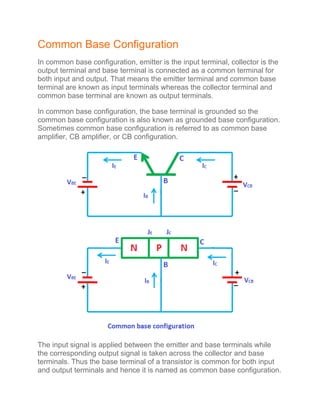
- 1. Common Base Configuration In common base configuration, emitter is the input terminal, collector is the output terminal and base terminal is connected as a common terminal for both input and output. That means the emitter terminal and common base terminal are known as input terminals whereas the collector terminal and common base terminal are known as output terminals. In common base configuration, the base terminal is grounded so the common base configuration is also known as grounded base configuration. Sometimes common base configuration is referred to as common base amplifier, CB amplifier, or CB configuration. The input signal is applied between the emitter and base terminals while the corresponding output signal is taken across the collector and base terminals. Thus the base terminal of a transistor is common for both input and output terminals and hence it is named as common base configuration.
- 2. The supply voltage between base and emitter is denoted by VBE while the supply voltage between collector and base is denoted by VCB. As mentioned earlier, in every configuration, the base-emitter junction JE is always forward biased and collector-base junction JC is always reverse biased. Therefore, in common base configuration, the base-emitter junction JE is forward biased and collector-base junction JC is reverse biased. The common base configuration for both NPN and PNP transistors is shown in the below figure. From the above circuit diagrams of npn and pnp transistors, it can be seen that for both npn and pnp transistors, the input is applied to the emitter and the output is taken from the collector. The common terminal for both the circuits is the base. Current flow in common base amplifier For the sake of understanding, let us consider NPN transistor in common base configuration.
- 3. The npn transistor is formed when a single p-type semiconductor layer is sandwiched between two n-type semiconductor layers. The base-emitter junction JE is forward biased by the supply voltage VBE while the collector-base junction JC is reverse biased by the supply voltage VCB. Due to the forward bias voltage VBE, the free electrons (majority carriers) in the emitter region experience a repulsive force from the negative terminal of the battery similarly holes (majority carriers) in the base region experience a repulsive force from the positive terminal of the battery. As a result, free electrons start flowing from emitter to base similarly holes start flowing from base to emitter. Thus free electrons which are flowing from emitter to base and holes which are flowing from base to emitter conducts electric current. The actual current is carried by free electrons which are flowing from emitter to base. However, we follow
- 4. the conventional current direction which is from base to emitter. Thus electric current is produced at the base and emitter region. The free electrons which are flowing from emitter to base will combine with the holes in the base region similarly the holes which are flowing from base to emitter will combine with the electrons in the emitter region. From the above figure, it is seen that the width of the base region is very thin. Therefore, only a small percentage of free electrons from emitter region will combine with the holes in the base region and the remaining large number of free electrons cross the base region and enters into the collector region. A large number of free electrons which entered into the collector region will experience an attractive force from the positive terminal of the battery. Therefore, the free electrons in the collector region will flow towards the positive terminal of the battery. Thus, electric current is produced in the collector region.
- 5. The electric current produced at the collector region is primarily due to the free electrons from the emitter region similarly the electric current produced at the base region is also primarily due to the free electrons from emitter region. Therefore, the emitter current is greater than the base current and collector current. The emitter current is the sum of base current and collector current. IE = IB + IC We know that emitter current is the input current and collector current is the output current. The output collector current is less than the input emitter current, so the current gain of this amplifier is actually less than 1. In other words, the common base amplifier attenuates the electric current rather than amplifying it. The base-emitter junction JE at input side acts as a forward biased diode. So the common base amplifier has a low input impedance (low opposition to incoming current). On the other hand, the collector-base junction JC at output side acts somewhat like a reverse biased diode. So the common base amplifier has high output impedance. Therefore, the common base amplifier provides a low input impedance and high output impedance. Transistors with low input impedance and high output impedance provide a high voltage gain. Even though the voltage gain is high, the current gain is very low and the overall power gain of the common base amplifier is low as compared to the other transistor amplifier configurations. The common base transistor amplifiers are primarily used in the applications where low input impedance is required. The common base amplifier is mainly used as a voltage amplifier or current buffer. This type of transistor arrangement is not very common and is not as widely used as the other two transistor configurations.
- 6. The working principle of pnp transistor with CB configuration is same as the npn transistor with CB configuration. The only difference is in npn transistor free electrons conduct most of the current whereas in pnp transistor the holes conduct most of the current. To fully describe the behavior of a transistor with CB configuration, we need two set of characteristics: they are Input characteristics Output characteristics. Input characteristics The input characteristics describe the relationship between input current (IE) and the input voltage (VBE). First, draw a vertical line and horizontal line. The vertical line represents y- axis and horizontal line represents x-axis. The input current or emitter current (IE) is taken along the y-axis (vertical line) and the input voltage (VBE)is taken along the x-axis (horizontal line). To determine the input characteristics, the output voltage VCB (collector- base voltage) is kept constant at zero volts and the input voltage VBE is increased from zero volts to different voltage levels. For each voltage level of the input voltage (VBE), the input current (IE) is recorded on a paper or in any other form. A curve is then drawn between input current IE and input voltage VBE at constant output voltage VCB (0 volts).
- 7. Next, the output voltage (VCB) is increased from zero volts to a certain voltage level (8 volts) and kept constant at 8 volts. While increasing the output voltage (VCB), the input voltage (VBE) is kept constant at zero volts. After we kept the output voltage (VCB) constant at 8 volts, the input voltage VBE is increased from zero volts to different voltage levels. For each voltage level of the input voltage (VBE), the input current (IE) is recorded on a paper or in any other form. A curve is then drawn between input current IE and input voltage VBE at constant output voltage VCB (8 volts). This is repeated for higher fixed values of the output voltage (VCB). When output voltage (VCB) is at zero volts and emitter-base junction JE is forward biased by the input voltage (VBE), the emitter-base junction acts like a normal p-n junction diode. So the input characteristics are same as the forward characteristics of a normal pn junction diode. The cut in voltage of a silicon transistor is 0.7 volts and germanium transistor is 0.3 volts. In our case, it is a silicon transistor. So from the
- 8. above graph, we can see that after 0.7 volts, a small increase in input voltage (VBE) will rapidly increase the input current (IE). When the output voltage (VCB) is increased from zero volts to a certain voltage level (8 volts), the emitter current flow will be increased which in turn reduces the depletion region width at emitter-base junction. As a result, the cut in voltage will be reduced. Therefore, the curves shifted towards the left side for higher values of output voltage VCB. Output characteristics The output characteristics describe the relationship between output current (IC) and the output voltage (VCB). First, draw a vertical line and a horizontal line. The vertical line represents y-axis and horizontal line represents x-axis. The output current or collector current (IC) is taken along the y-axis (vertical line) and the output voltage (VCB)is taken along the x-axis (horizontal line). To determine the output characteristics, the input current or emitter current IE is kept constant at zero mA and the output voltage VCB is increased from zero volts to different voltage levels. For each voltage level of the output voltage VCB, the output current (IC) is recorded. A curve is then drawn between output current IC and output voltage VCB at constant input current IE (0 mA). When the emitter current or input current IE is equal to 0 mA, the transistor operates in the cut-off region.
- 9. Next, the input current (IE) is increased from 0 mA to 1 mA by adjusting the input voltage VBE and the input current IE is kept constant at 1 mA. While increasing the input current IE, the output voltage VCB is kept constant. After we kept the input current (IE) constant at 1 mA, the output voltage (VCB) is increased from zero volts to different voltage levels. For each voltage level of the output voltage (VCB), the output current (IC) is recorded. A curve is then drawn between output current IC and output voltage VCB at constant input current IE (1 mA). This region is known as the active region of a transistor. This is repeated for higher fixed values of input current IE (I.e. 2 mA, 3 mA, 4 mA and so on). From the above characteristics, we can see that for a constant input current IE, when the output voltage VCB is increased, the output current IC remains constant. At saturation region, both emitter-base junction JE and collector-base junction JC are forward biased. From the above graph, we can see that a
- 10. sudden increase in the collector current when the output voltage VCB makes the collector-base junction JC forward biased. Early effect Due to forward bias, the base-emitter junction JE acts as a forward biased diode and due to reverse bias, the collector-base junction JC acts as a reverse biased diode. Therefore, the width of the depletion region at the base-emitter junction JE is very small whereas the width of the depletion region at the collector- base junction JC is very large. If the output voltage VCB applied to the collector-base junction JC is further increased, the depletion region width further increases. The base region is lightly doped as compared to the collector region. So the depletion region penetrates more into the base region and less into the collector region. As a result, the width of the base region decreases. This dependency of base width on the output voltage (VCB) is known as an early effect. If the output voltage VCB applied to the collector-base junction JC is highly increased, the base width may be reduced to zero and causes a voltage breakdown in the transistor. This phenomenon is known as punch through. Transistor parameters Dynamic input resistance (ri) Dynamic input resistance is defined as the ratio of change in input voltage or emitter voltage (VBE) to the corresponding change in input current or emitter current (IE), with the output voltage or collector voltage (VCB) kept at constant. The input resistance of common base amplifier is very low. Dynamic output resistance (ro)
- 11. Dynamic output resistance is defined as the ratio of change in output voltage or collector voltage (VCB) to the corresponding change in output current or collector current (IC), with the input current or emitter current (IE) kept at constant. The output resistance of common base amplifier is very high. Current gain (α) The current gain of a transistor in CB configuration is defined as the ratio of output current or collector current (IC) to the input current or emitter current (IE). The current gain of a transistor in CB configuration is less than unity. The typical current gain of a common base amplifier is 0.98.
- 12. Common Collector Configuration In this configuration, the base terminal of the transistor serves as the input, the emitter terminal is the output and the collector terminal is common for both input and output. Hence, it is named as common collector configuration. The input is applied between the base and collector while the output is taken from the emitter and collector. In common collector configuration, the collector terminal is grounded so the common collector configuration is also known as grounded collector configuration.
- 13. Sometimes common collector configuration is also referred to as emitter follower, voltage follower, common
- 14. collector amplifier, CC amplifier, or CC configuration. This configuration is mostly used as a voltage buffer. The input supply voltage between base and collector is denoted by VBC while the output voltage between emitter and collector is denoted by VEC . In this configuration, input current or base current is denoted by IB and output current or emitter current is denoted by IE .The common collector amplifier has high input impedance and low output impedance. It has low voltage gain and high current gain. The power gain of the common collector amplifier is medium. To fully describe the behavior of a transistor with CC configuration, we need two set of characteristics - input characteristics and output characteristics. Input characteristics The input characteristics describe the relationship between input current or base current (IB ) and input voltage or base-collector voltage (VBC ). First, draw a vertical line and a horizontal line. The vertical line represents y-axis and horizontal line represents x-ax The input current or base current (IB ) is taken along y-axis (vertical line) and the input voltage or base-collector voltage (VBC ) is taken along x-axis (horizontal line).
- 15. To determine the input characteristics, the output voltage VEC is kept constant at 3V and the input voltage VBC is increased from zero volts to different voltage levels. For each level of input voltage VBC, the corresponding input current IB is noted. A curve is then drawn between input current IB and input voltage VBC at constant output voltage VEC (3V). Next, the output voltage VEC is increased from 3V to different voltage level, say for example 5V and then kept constant at 5V. While increasing the output voltage VEC , the input voltage VBC is kept constant at zero volts. After we kept the output voltage VEC constant at 5V, the input voltage VBC is increased from zero volts to different voltage levels. For each level of input voltage VBC , the corresponding input current IB is noted. A curve is then
- 16. drawn between input current IB and input voltage VBC at constant output voltage VEC (5V). This process is repeated for higher fixed values of output voltage (VEC ). Output characteristics The output characteristics describe the relationship between output current or emitter current (IE ) and output voltage or emitter-collector voltage (VEC ). First, draw a vertical line and a horizontal line. The vertical line represents y-axis and horizontal line represents x- axis. The output current or emitter current (IE ) is taken along y- axis (vertical line) and the output voltage or emitter- collector voltage (VEC ) is taken along x-axis (horizontal line). To determine the output characteristics, the input current IB is kept constant at zero micro amperes and the output voltage VEC is increased from zero volts to different voltage levels. For each level of output voltage VEC , the corresponding output current IE is noted. A curve is then drawn between output current IE and output voltage VEC at constant input current IB (0 μA).
- 17. Next, the input current (IB ) is increased from 0 μA to 20 μA and then kept constant at 20 μA. While increasing the input current (IB ), the output voltage (VEC ) is kept constant at 0 volts. After we kept the input current (IB ) constant at 20 μA, the output voltage (VEC ) is increased from zero volts to different voltage levels. For each level of output voltage (VEC ), the corresponding output current (IE ) is recorded. A curve is then drawn between output current IE and output voltage VEC at constant input current IB (20μA). This region is known as the active region of a transistor. This process is repeated for higher fixed values of input current IB (I.e. 40 μA, 60 μA, 80 μA and so on).
- 18. In common collector configuration, if the input current or base current is zero then the output current or emitter current is also zero. As a result, no current flows through the transistor. So the transistor will be in the cutoff region. If the base current is slightly increased then the output current or emitter current also increases. So the transistor falls into the active region. If the base current is heavily increased then the current flowing through the transistor also heavily increases. As a result, the transistor falls into the saturation region. Transistor parameters Dynamic input resistance (ri) Dynamic input resistance is defined as the ratio of change in input voltage or base voltage (VBC ) to the corresponding change in input current or base current (IB ), with the output voltage or emitter voltage (VEC ) kept at constant. The input resistance of common collector amplifier is high. Dynamic output resistance (ro) Dynamic output resistance is defined as the ratio of change in output voltage or emitter voltage (VEC ) to the corresponding change in output current or emitter current (IE ), with the input current or base current (IB ) kept at constant. The output resistance of common collector amplifier is low.
- 19. Current amplification factor (γ) The current amplification factor is defined as the ratio of change in output current or emitter current IE to the change in input current or base current IB . It is expressed by γ. The current gain of a common collector amplifier is high.