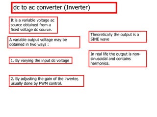
1. A variable output voltage can be obtained from an inverter in two ways: by varying the input DC voltage or by adjusting the gain of the inverter using pulse width modulation control.
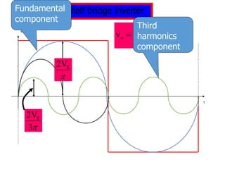
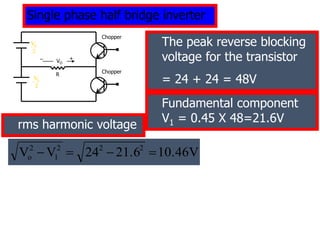
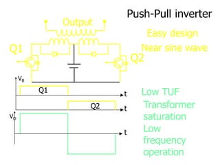
2. The output of an inverter is theoretically a sine wave but in reality is non-sinusoidal and contains harmonics that can be represented by Fourier series.
3. The fundamental component of the output voltage determines the useful power while harmonic components cause power loss and increased load temperature.