This document discusses the bipolar junction transistor (BJT) including:
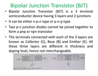
- Its structure as a 3-terminal semiconductor device with 3 layers and 2 junctions.
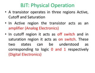
- Its 3 operating regions: active, cutoff, and saturation.
- Different configurations including common emitter, collector, and base modes.
- Key parameters like current gains and reverse saturation currents.
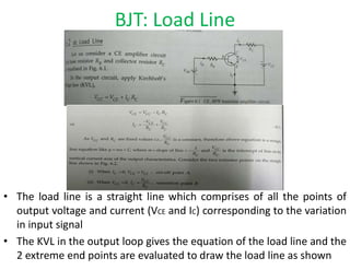
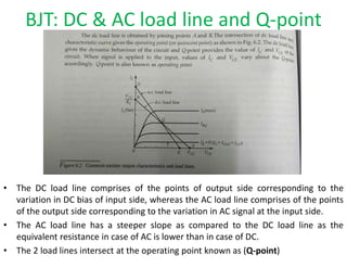
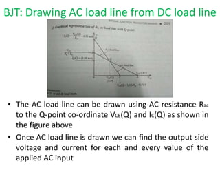
- Drawing load lines and setting the operating point to design BJT amplifiers.
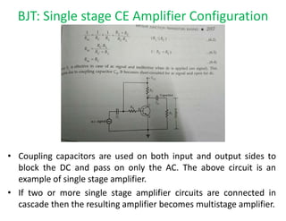
- Single stage common emitter amplifier configuration using coupling capacitors.
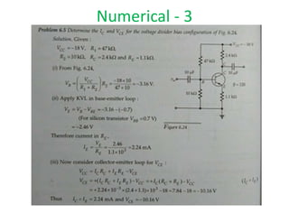
- Numerical examples calculating voltages and currents in BJT circuits.