Downloaded 684 times


This document discusses junction transistors and semiconductor devices. It describes the basic structure and operation of NPN and PNP transistors, including how current flows when the emitter-base and collector-base junctions are forward and reverse biased. It also explains the characteristics of transistors in common base and common emitter configurations, including the phase relationships between input and output signals. Finally, it defines various gains such as current gain, voltage gain, and transconductance.
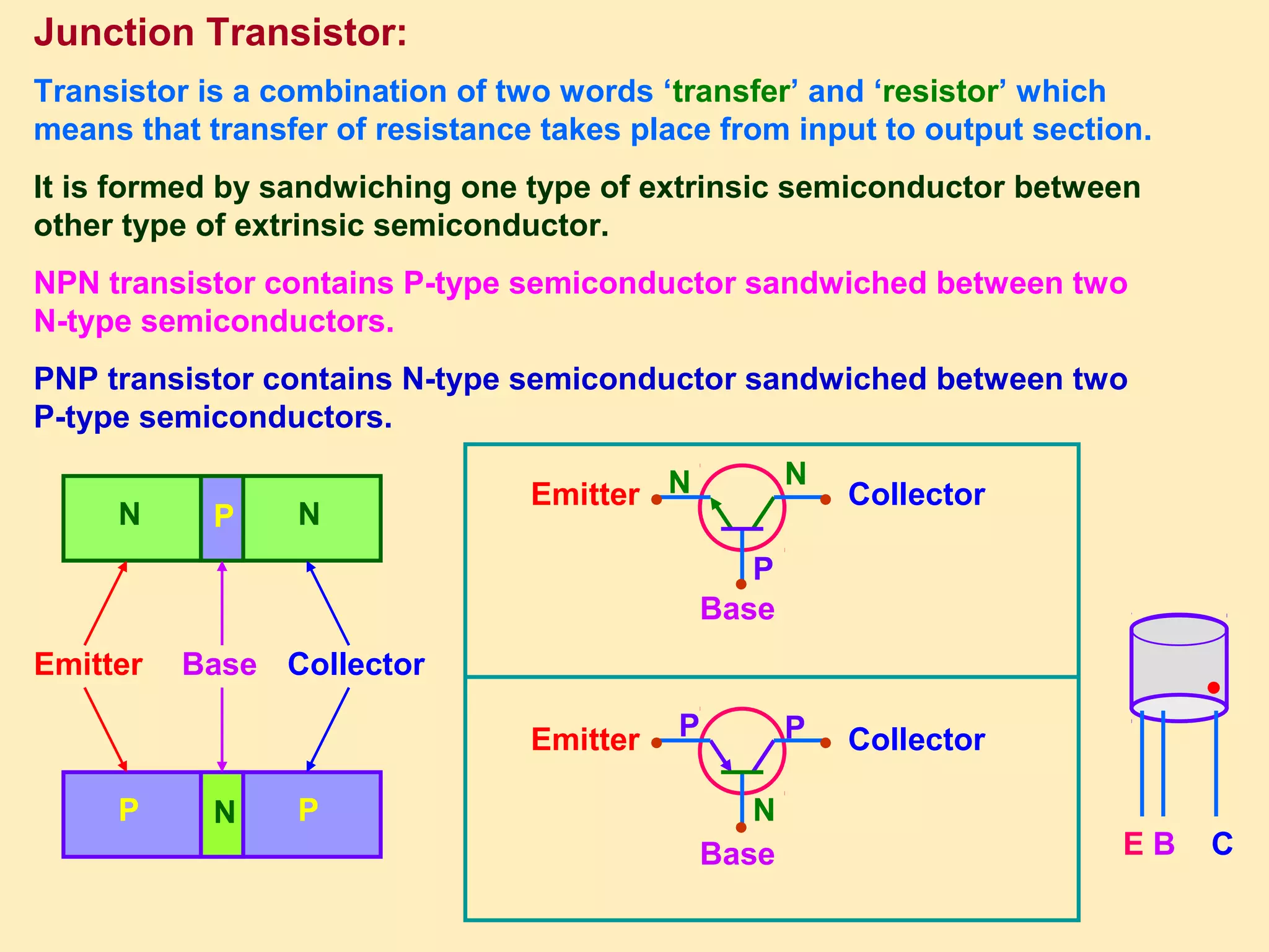
Introduction to junction transistors, concepts of NPN and PNP transistors, and their configurations.
NPN and PNP transistors explained as combinations of semiconductor types, illustrating structure and current flow.
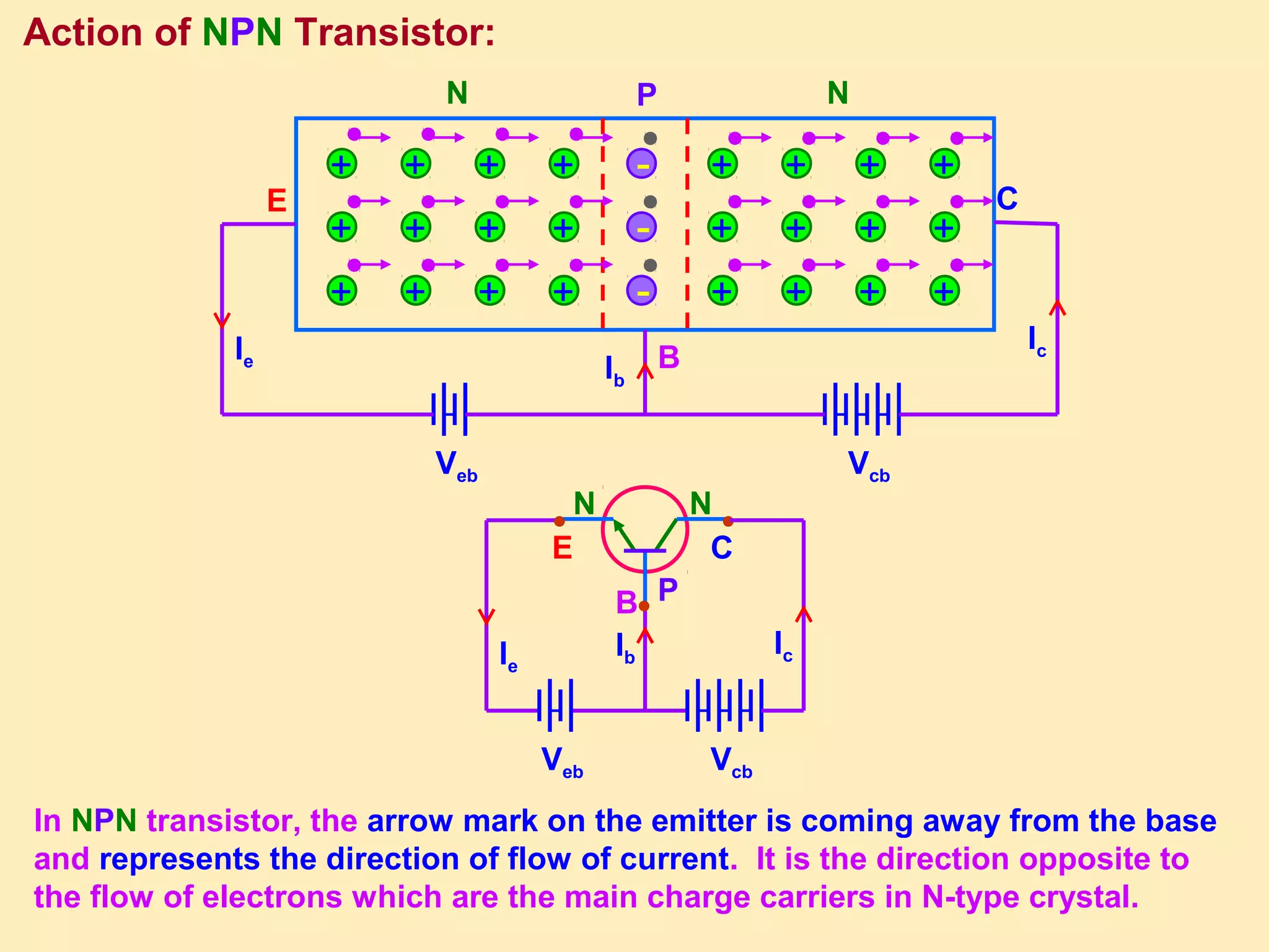
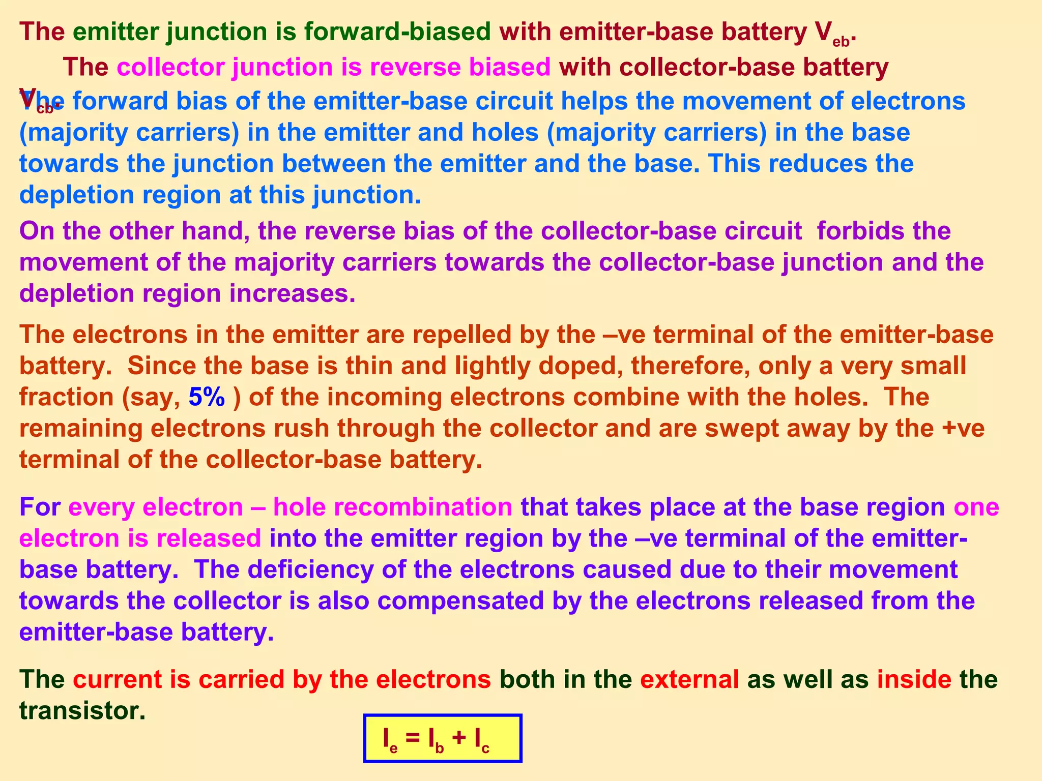
Details on the operation of NPN transistors focusing on current flow, electron movement, and relations Ie, Ib, Ic.
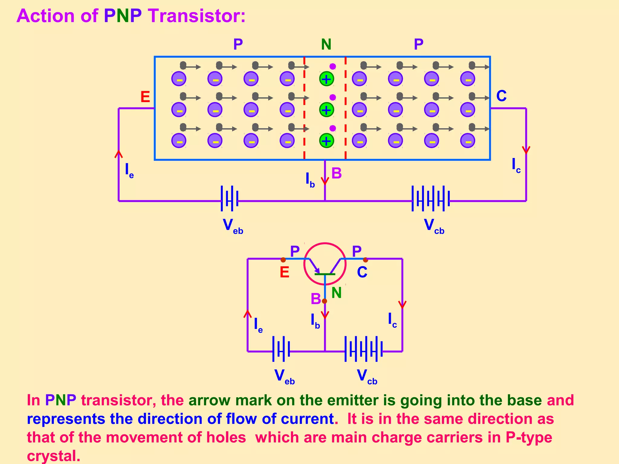
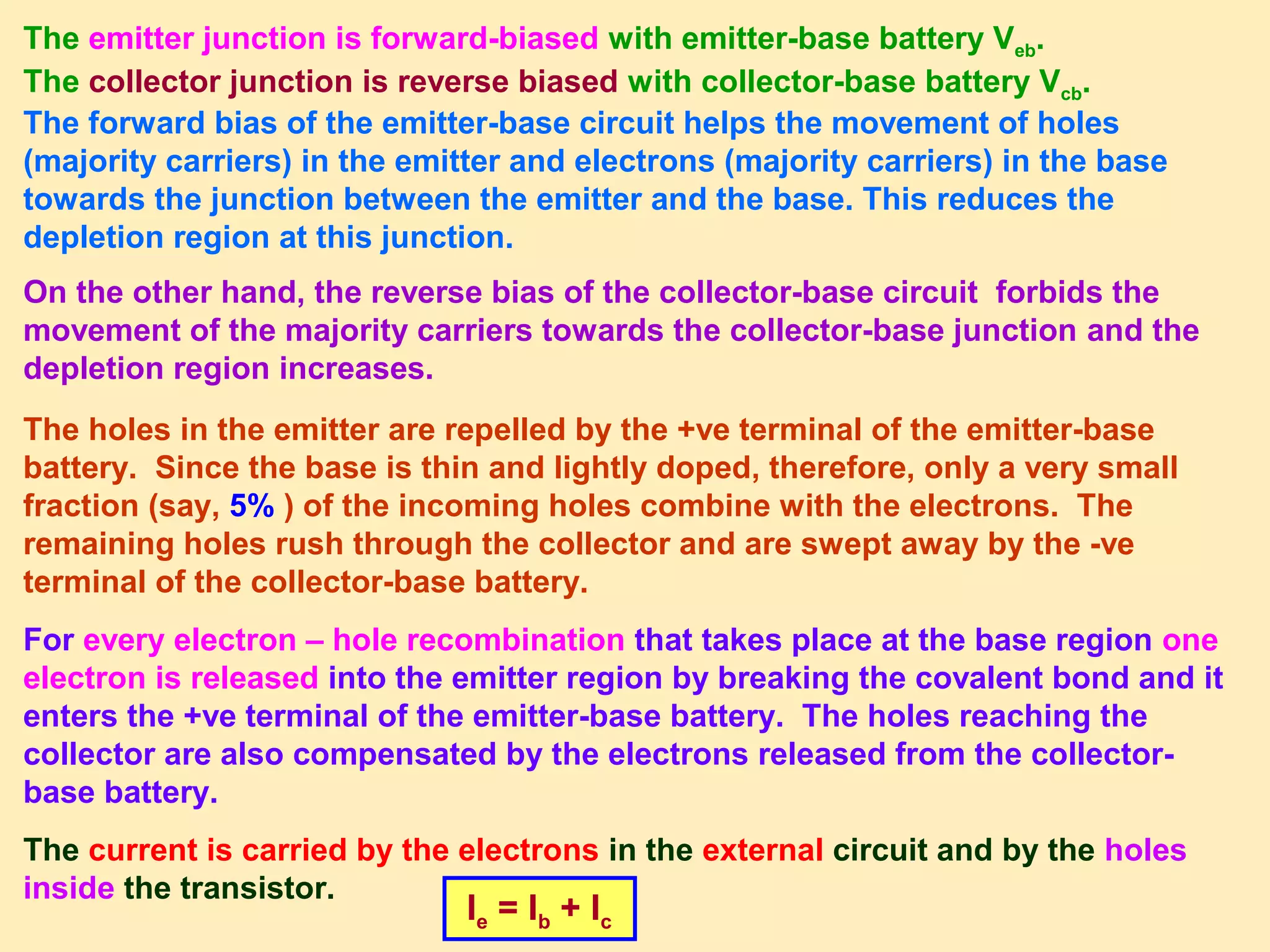
Describes PNP transistor operations, emphasizing hole movement, current relations similar to NPN.
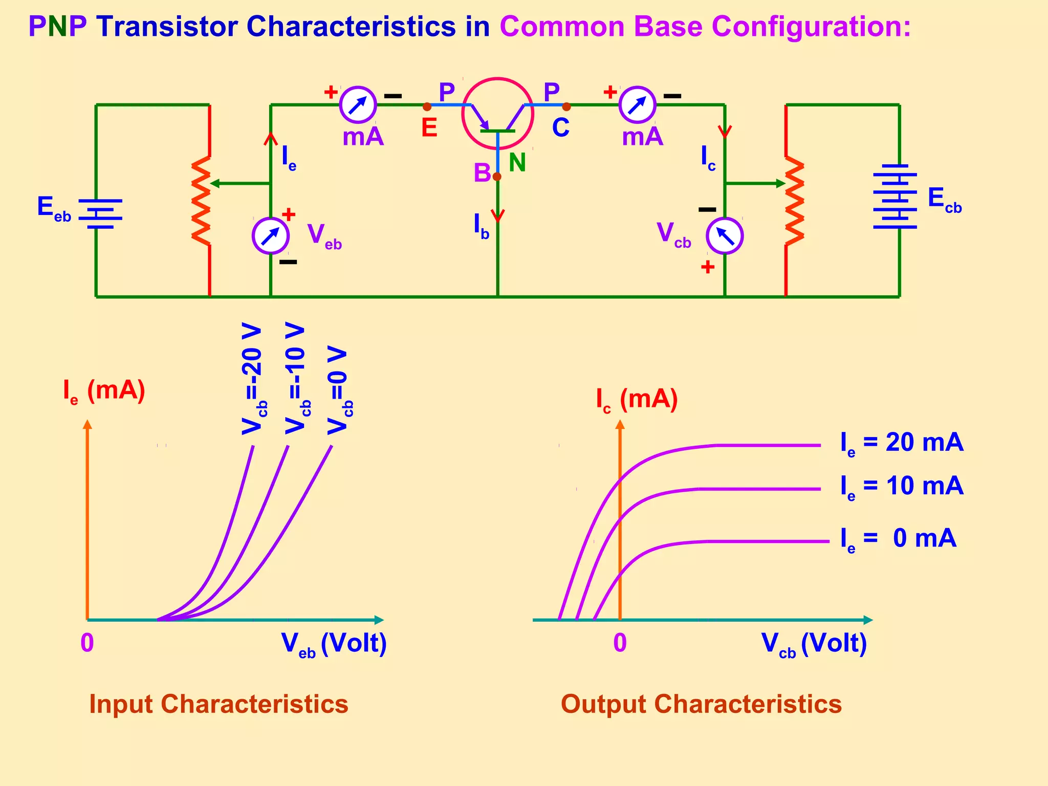
Characteristics of PNP transistors in common base and emitter configurations, including input/output graphs.
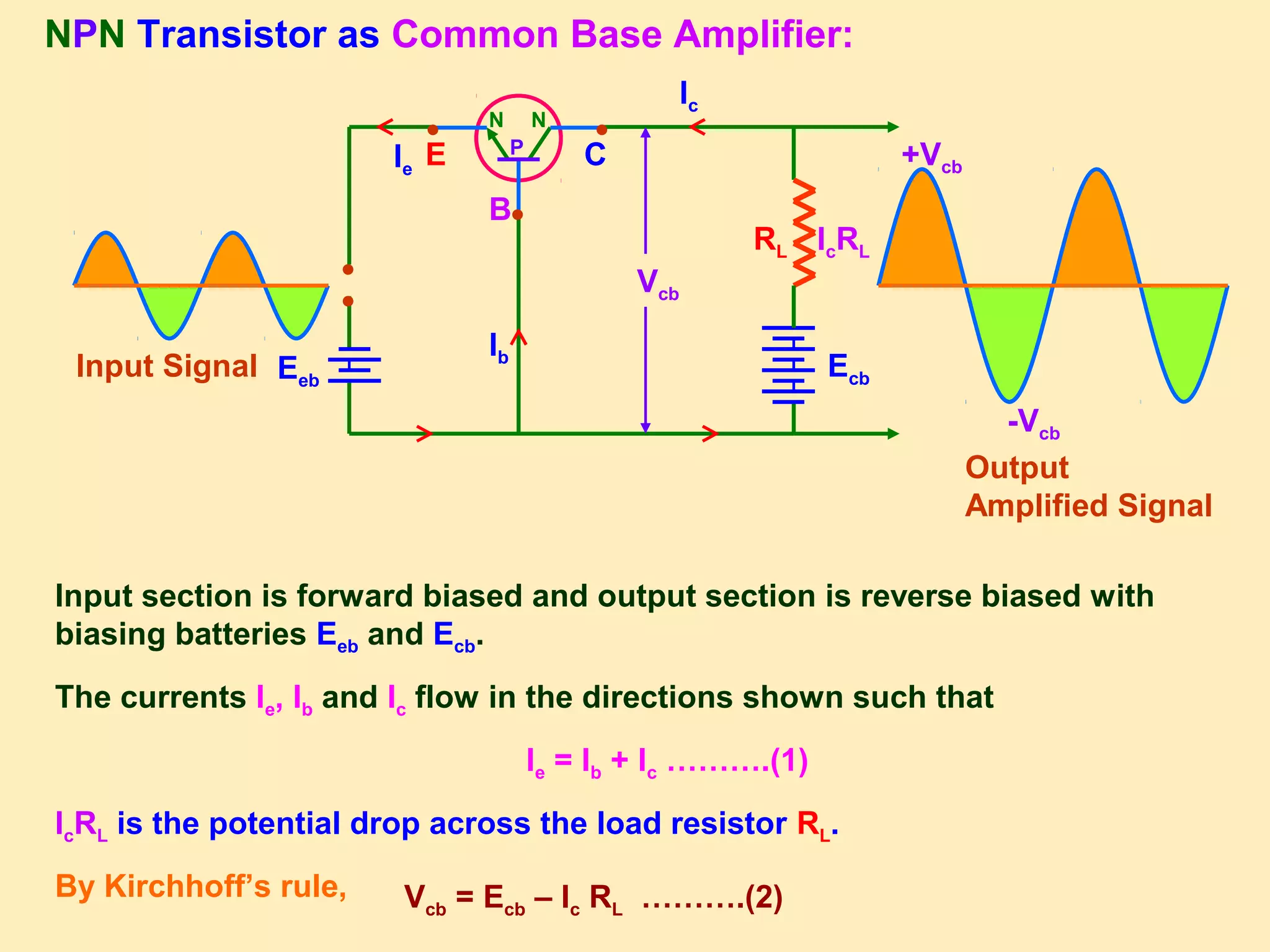
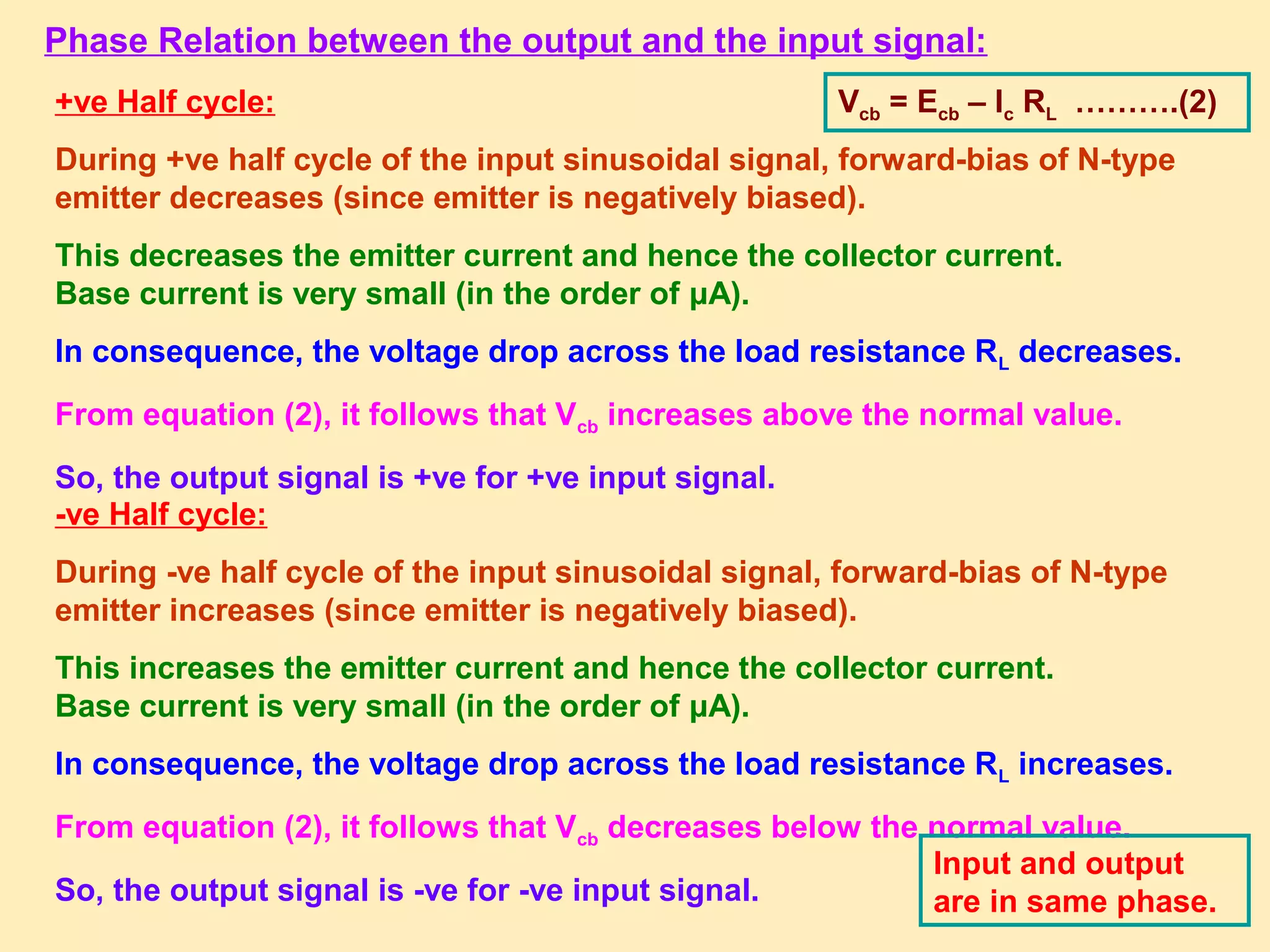
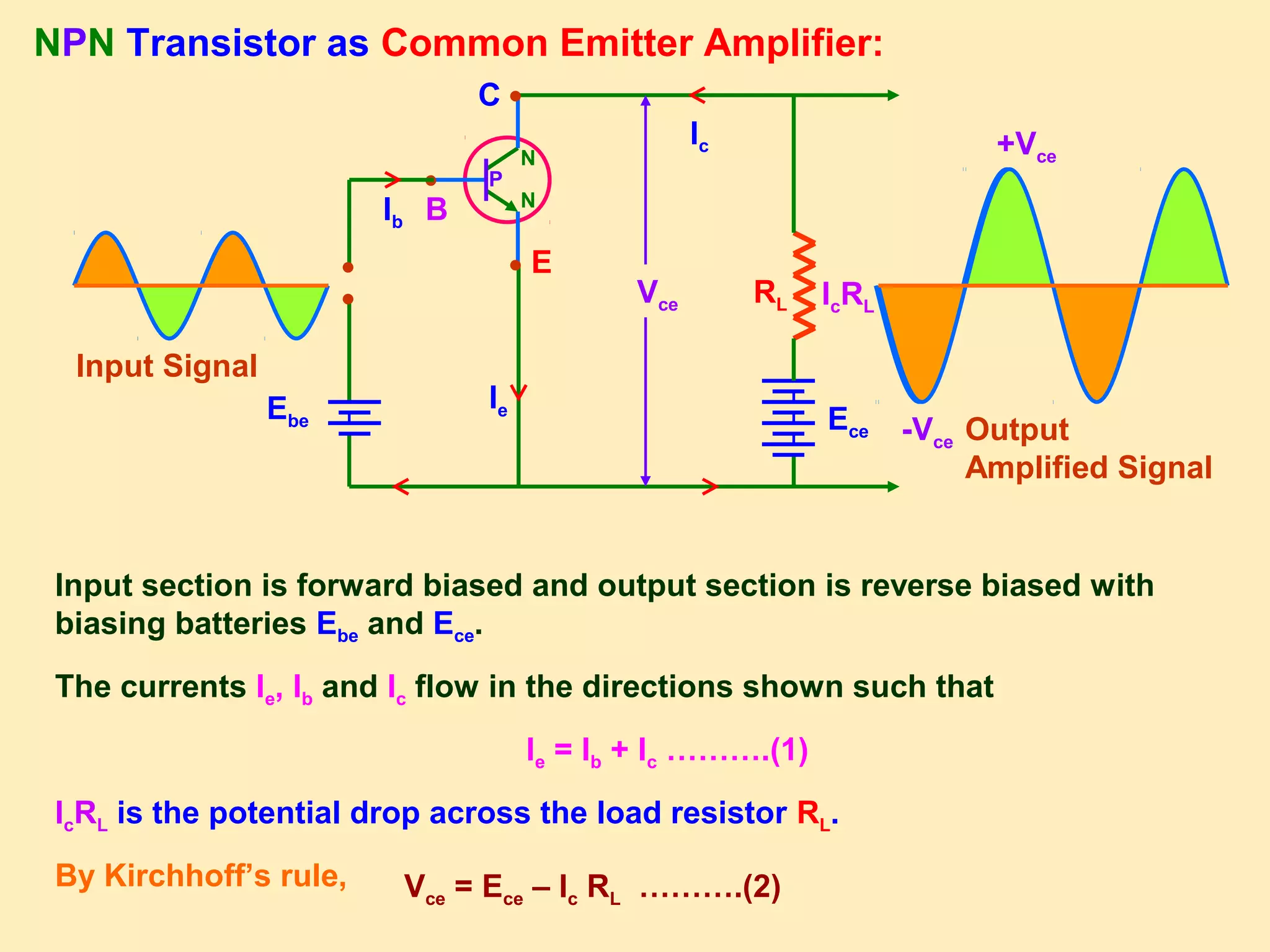
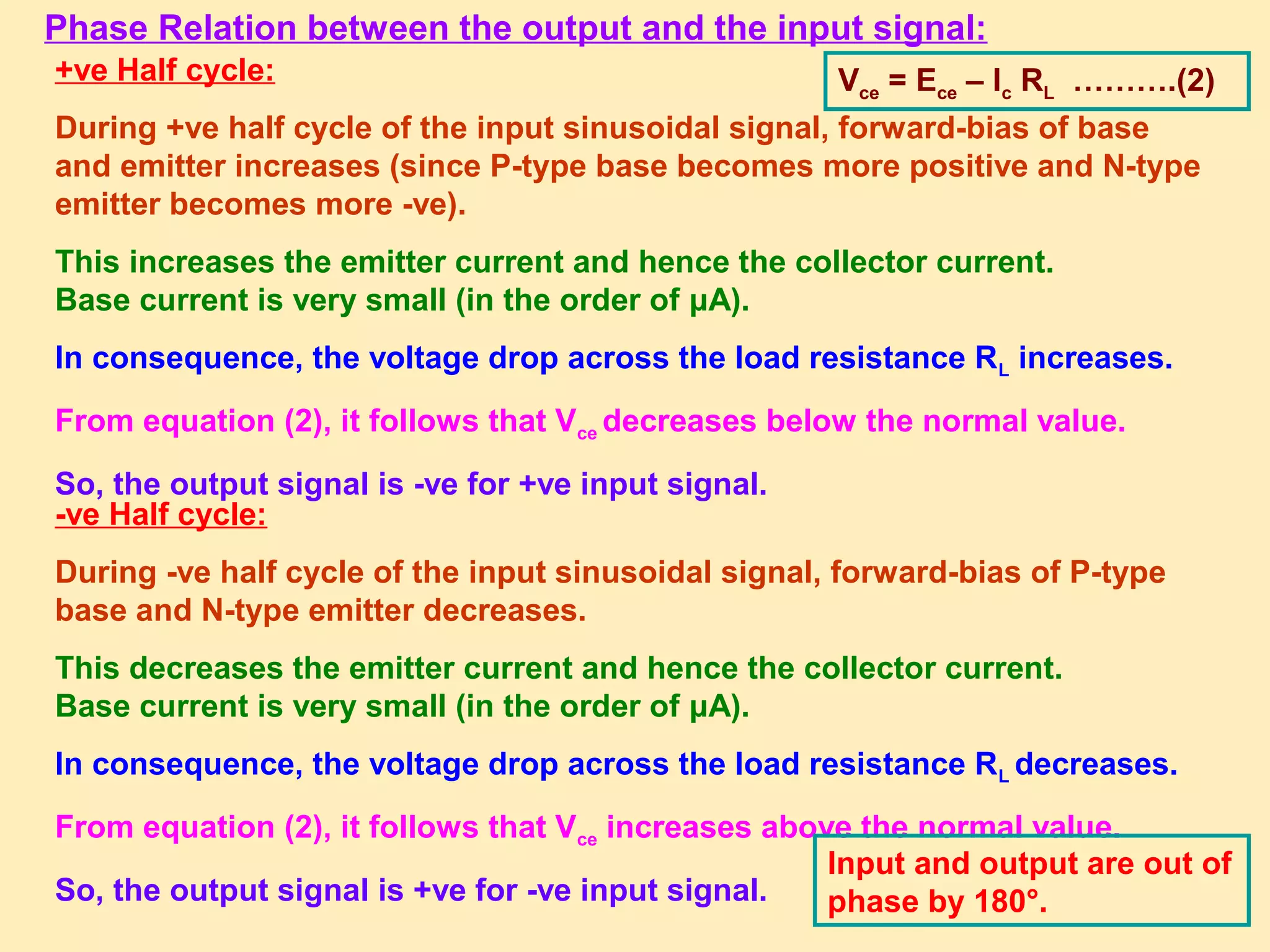
Describes NPN transistor amplifiers, input/output relations, phase inversions during signal cycles.
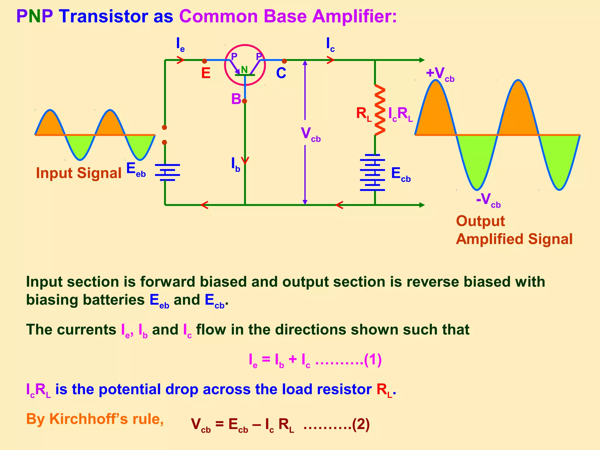
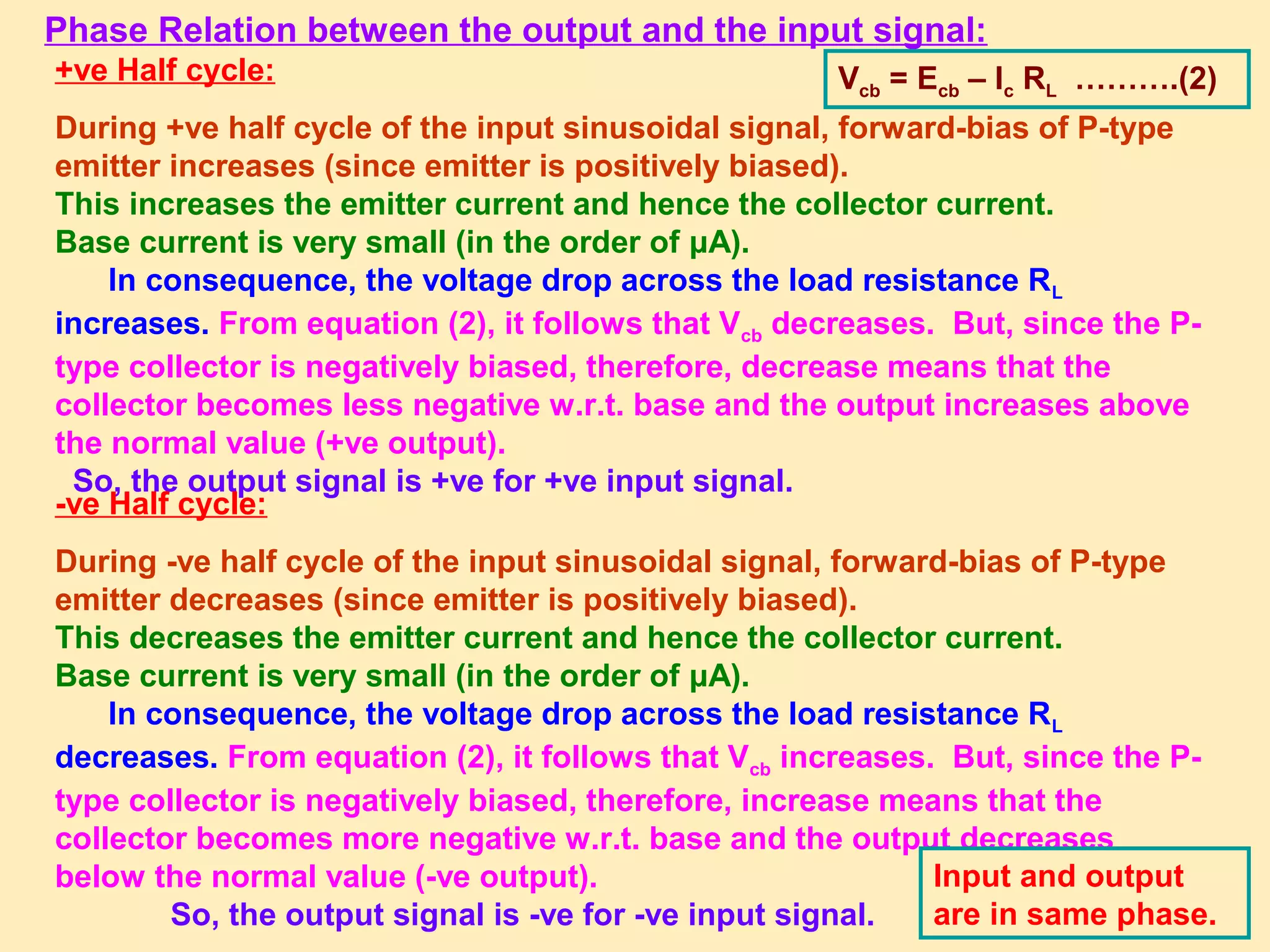
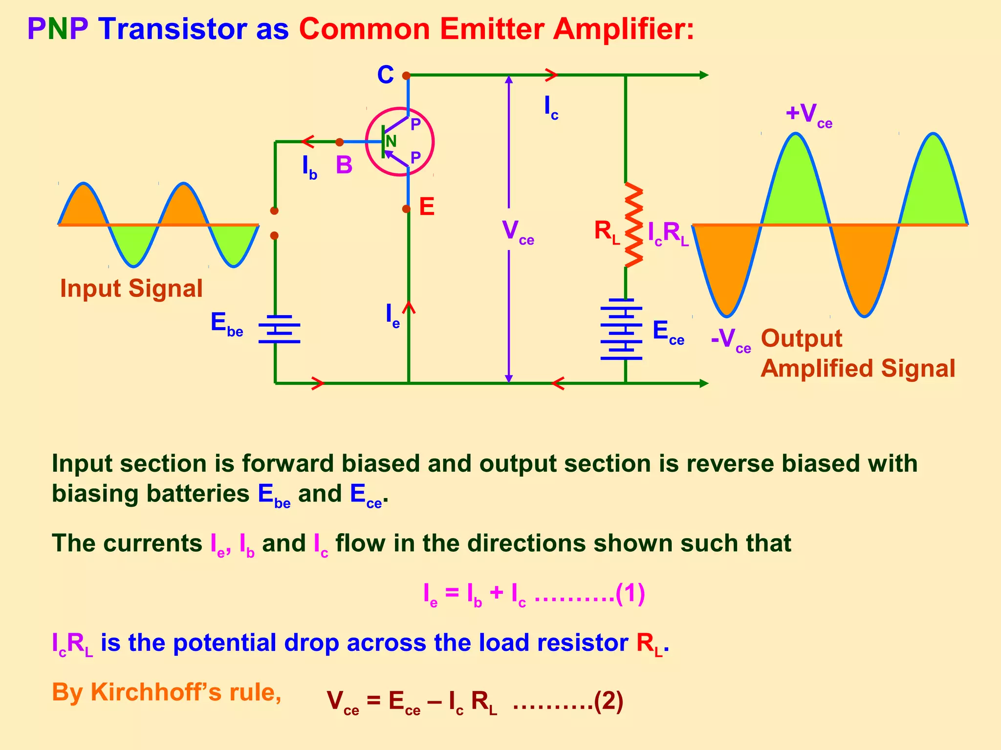
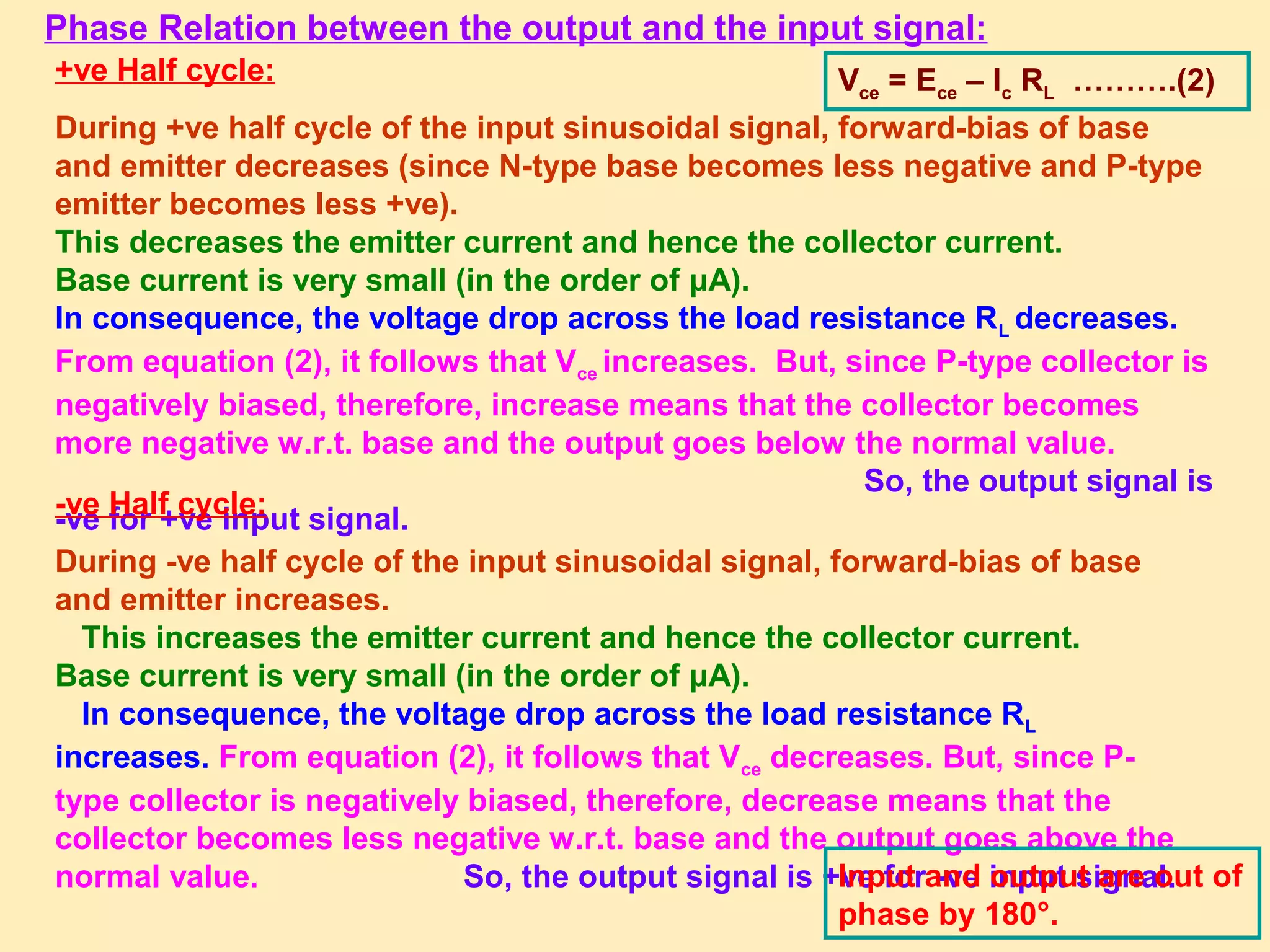
Detailed operations of PNP transistors as amplifiers, phase relation of output during input signal changes.
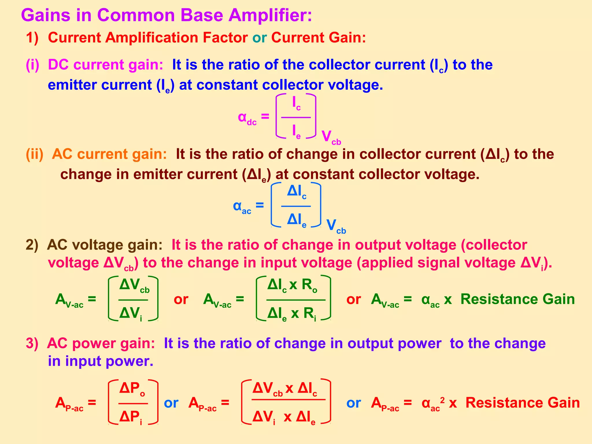
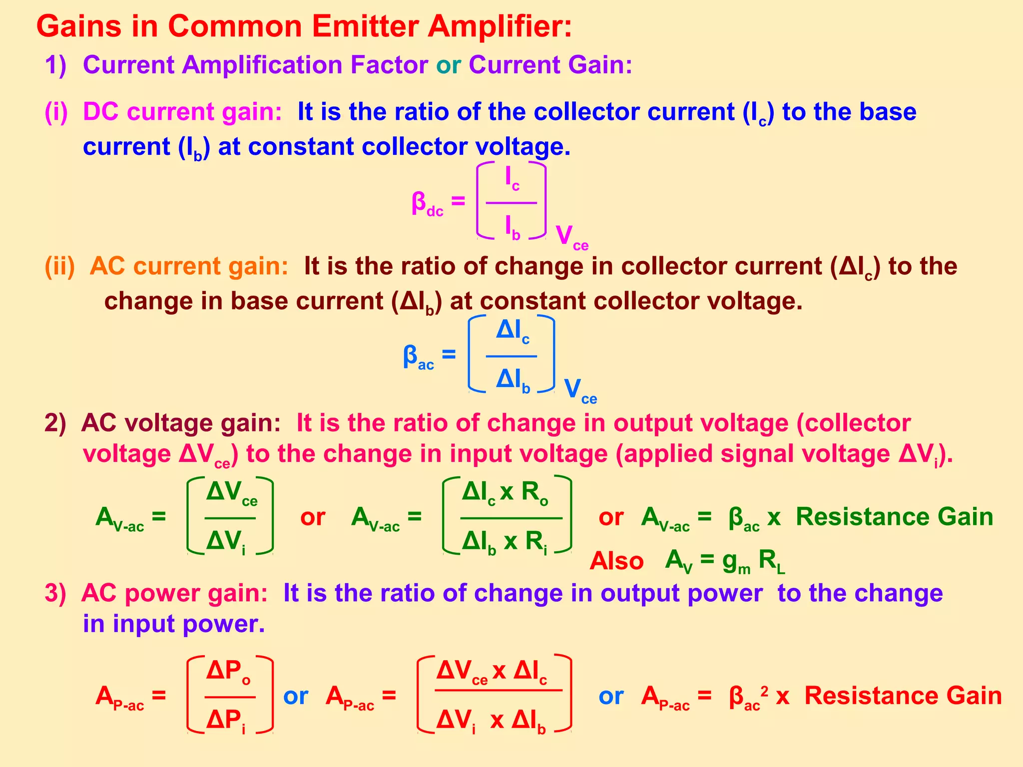
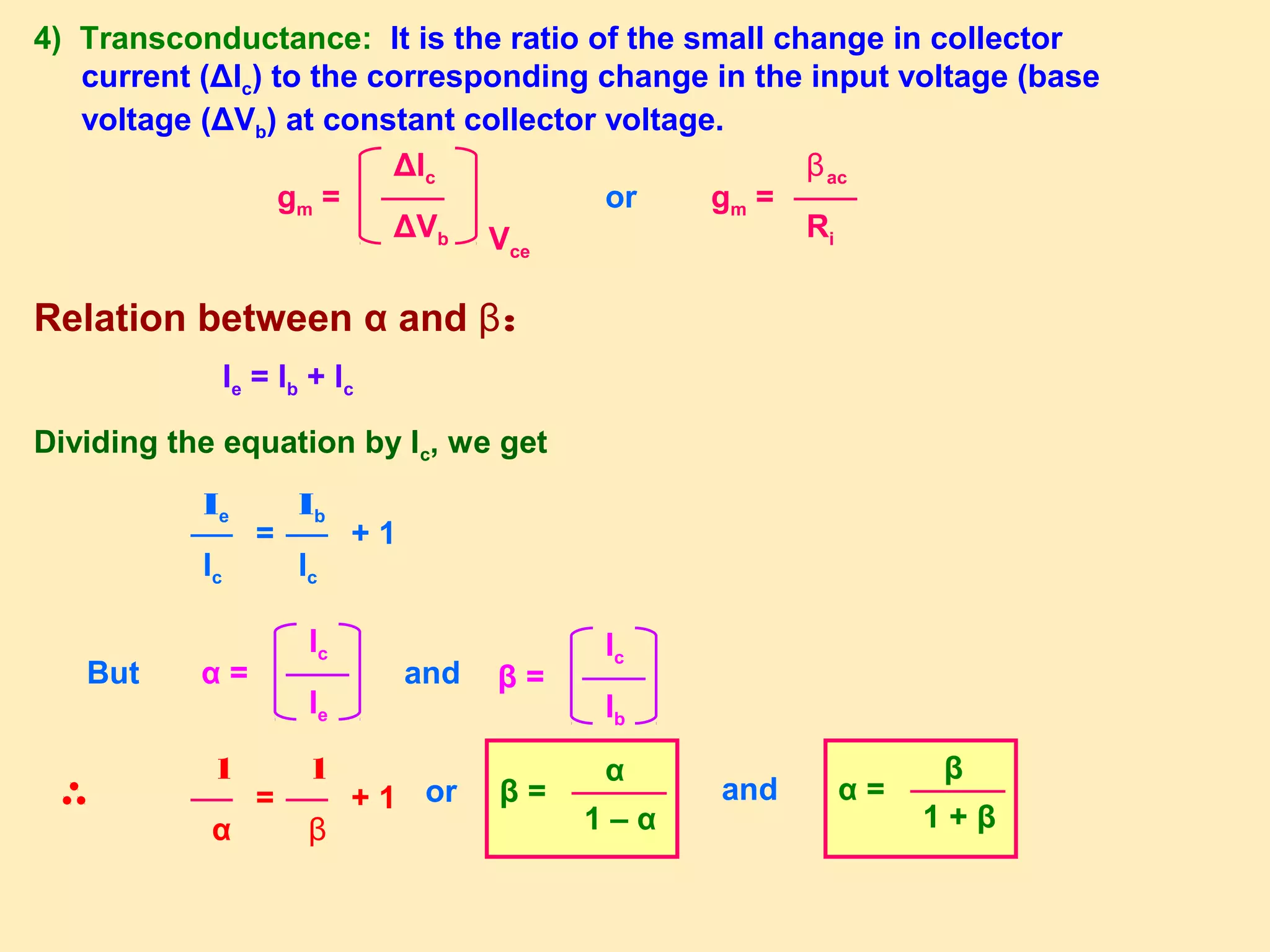
Gains defined such as current amplification factors, voltage and power gain, including mathematical expressions.
NPN common emitter amplifiers explained, emphasizing output signal phases and their relation to input.
Functions of PNP common emitter amplifiers with detailed signal phase relations and behaviors.
Definitions for current amplification factor and transconductance with equations for better understanding.
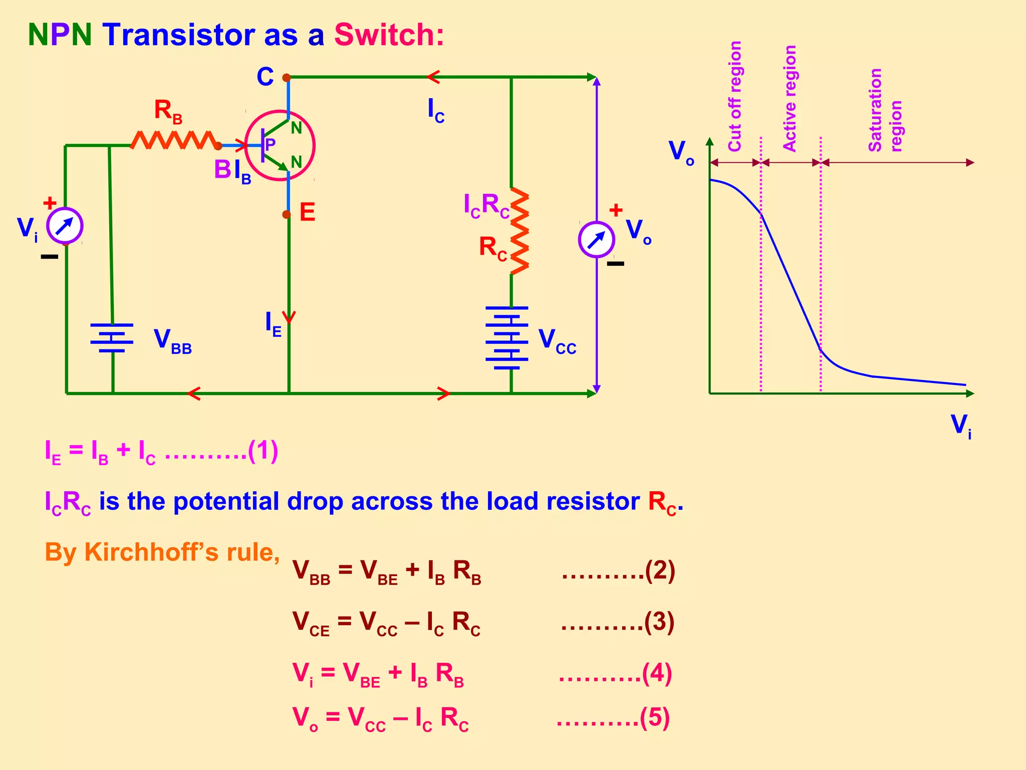
Application of transistors as switches, detailing the active, cutoff, and saturation regions with Kirchhoff's rules.
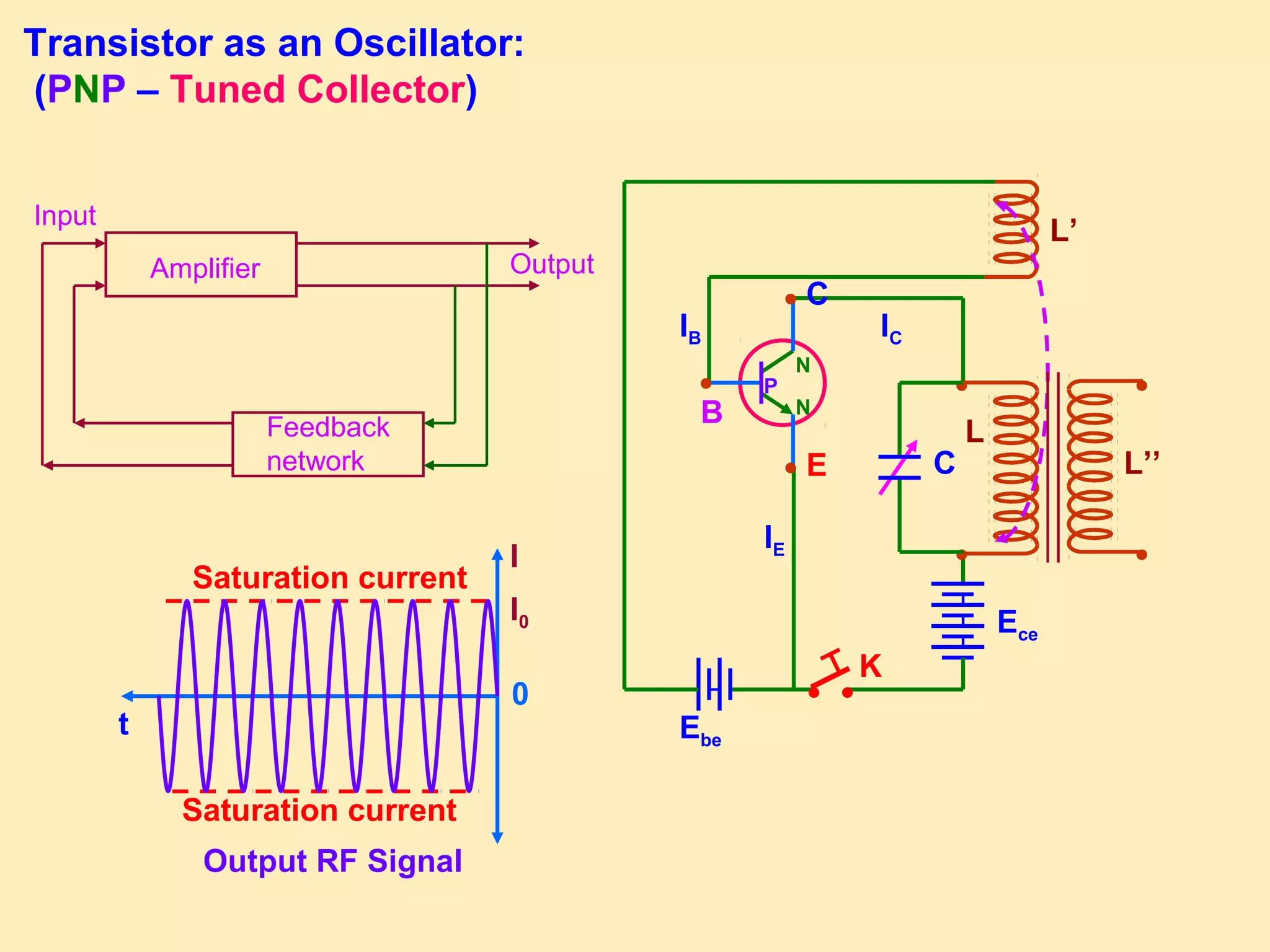
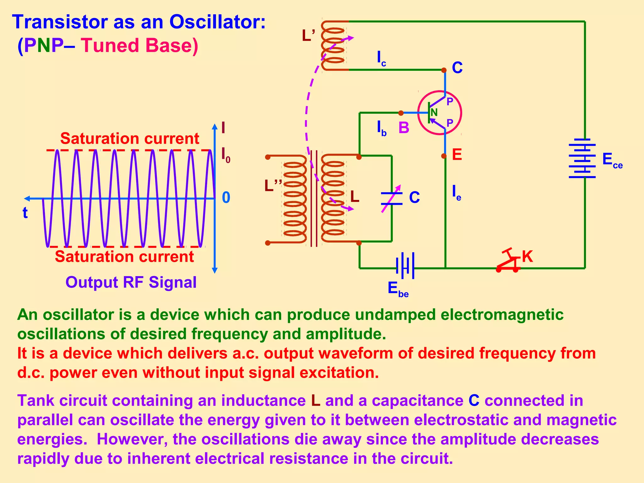
Introduction to transistor oscillators, functionality overview and principles of producing undamped oscillations.
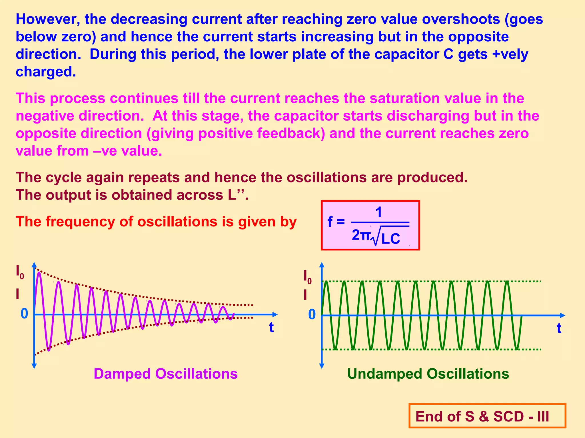
Mechanism of how transistors provide positive feedback in oscillation, explaining current behavior and cycles.
Mathematics related to oscillation frequencies in tuned circuits, emphasizing the role of inductance and capacitance.


