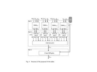
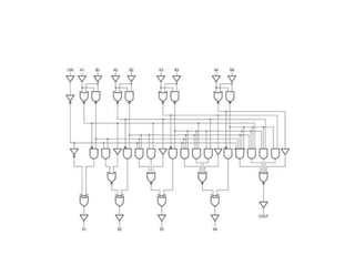
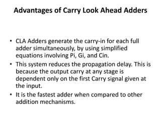
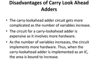
PRESENTATION ON
Carry Maskable look ahead adder
for approixmate computing
GUIDE PRESENTED BY
objective
• The objective of this work is to present a new
look ahead adder design circuits combined
with carry mask
• To enhance the performance of adder by
reducing the propagation delay, area on chip
& reducing the complexity of circuit.
introduction
The proposed adder is based on the
conventional carry look-ahead adder, and its
configurability of accuracy is realized by
masking the carry propagation at runtime.
Compared with the conventional carry look-
ahead adder.
CLA
• Typically, a CLA consists of three parts: (1) half
adders for carry generation (G) and
propagation (P) signals preparation,(2) carry
look-ahead units for carry generation, and (3)
XOR gates for sum generation
• Pi = Ai⨁Bi, Gi= Ai ⋅ B i (1)
• Ci= Gi + Pi ⋅ C i-1 (2)
• S i= Pi⨁C i-1 (3)
where i is denoted the bit position from the least
significant bit ,Note that owing to reuse of the circuit of Ai XOR Bi for Si
generation, here Pi is defined as Ai XOR Bi instead of Ai OR
Bi.Because C0 is equal to G0 , if G0 is 0, C0 will be0.From (2), we find that
C1 is equal to G1 when C0 is 0. In other words, if G0 and G1 are equal to
0, C0 and C1 will be 0.
• So By expanding the above to i , Ci will be 0 when G0, G1, … , Gi are all 0.
This means that the carry propagation from C0 to Ci is masked. From (3),
we can obtain that Si is equal to Pi when Ci-1 is 0.
if G is controllable and can be controlled to be 0, the carry propagation
will be masked and S (=P) can be considered as an approximate
sum. In other words, we can obtain the selectivity of S between
the accurate and approximate sum if we can control G to be A
AND B or 0. Evidently, we can achieve selectivity by adding a
select signal. Figure 1(a) is a conventional half adder and Fig.
1(b) is a half adder to which the select signal has been added.
Compared with the conventional half adder, we add a signal
named “M_X” as the select signal and use a 3-input AND gate
to replace the 2-input one. When M_X = 1, the function of G is
the same as that of a conventional half adder; when M_X = 0, G
is equal to 0.
Carry maskable half adder
Toward better accuracy results for the approximate sum, we use an OR
function instead
of an XOR function for P generation when M_X = 0. Thus, the
difference will be reduced to 1. A 2-input XOR gate can be
implemented by using a 2-input NAND gate, a 2-input OR gate,
and a 2-input AND gate. An equivalent circuit of the
conventional half adder is shown in Fig. 2. This is called a
carrymaskable half adder (CMHA). The dashed frame represents
the equivalent circuit of a 2-input XOR (M_X = 1). We can obtain
the following: P is equal to A XOR B, and G is equal to A AND
B when M_X = 1; when M_X = 0, P is equal to A OR B and G
is 0. Thus, M_X can be considered as a carry mask signal.
Carry maskable half adder
CMHA
Four groups (CMHA3-0, CMHA7-4, CMHA11-
8, and CMHA15-12) are used to prepare the P and G signals. Each
group comprises four CMHAs There is no mask signal for
CMHA15-12 in this example; therefore, accurate P15-12 (= A15-12
XOR B15-12) and G15-12 (= A15-12 AND B15-12) are always
obtained. P15-0 and G15-0 are the outputs from Part 1 and are
connected to Part 2. Note that P15-0 is also connected to Part 3
for sum generation. In Part 2, four 4-bit carry look-ahead units
(unit 0, 1, 2, 3) generate four PGs (PG0, PG1, PG2, and PG3),
four GGs (GG0, GG1, GG2, and GG3), and 12 carries (C2-0, C6-
4, C10-8, and C14-12) first, and then the carry look-ahead unit 4
generates the remaining four carries (C3, C7, C11, and C15) by
using the PGs and GGs. C15-0 is the output of Part 2 and is
connected to Part 3. The fifteen 2-input XOR gates in Part 3
generate the sum.
Advantages of Carry Look Ahead Adders
• CLA Adders generate the carry-in for each full
adder simultaneously, by using simplified
equations involving Pi, Gi, and Cin.
• This system reduces the propagation delay. This is
because the output carry at any stage is
dependent only on the first Carry signal given at
the input.
• It is the fastest adder when compared to other
addition mechanisms.
Disadvantages of Carry Look Ahead
Adders
• The carry-lookahead adder circuit gets more
complicated as the number of variables increase.
• The circuit for a carry-lookahead adder is
expensive as it involves more hardware.
• As the number of variables increases, the circuit
implements more hardware. Thus, when the
carry-lookahead adder is implemented as an IC,
the area is bound to increase.
Conclusion
without suffering the cost of the increase in
power or in delay for configurability was
proposed. The proposed adder is based on the
conventional CLA, and its configurability of
accuracy is realized by masking the carry pro
pagation at runtime. The experimental results
demonstrate that the proposed adder delivers
significant power savings and speedup with a
small area overhead than those of the
conventional CLA.

carry maskable look ahead adder for approximate computing

  • 1.
    PRESENTATION ON Carry Maskablelook ahead adder for approixmate computing GUIDE PRESENTED BY
  • 2.
    objective • The objectiveof this work is to present a new look ahead adder design circuits combined with carry mask • To enhance the performance of adder by reducing the propagation delay, area on chip & reducing the complexity of circuit.
  • 3.
    introduction The proposed adderis based on the conventional carry look-ahead adder, and its configurability of accuracy is realized by masking the carry propagation at runtime. Compared with the conventional carry look- ahead adder.
  • 4.
    CLA • Typically, aCLA consists of three parts: (1) half adders for carry generation (G) and propagation (P) signals preparation,(2) carry look-ahead units for carry generation, and (3) XOR gates for sum generation
  • 5.
    • Pi =Ai⨁Bi, Gi= Ai ⋅ B i (1) • Ci= Gi + Pi ⋅ C i-1 (2) • S i= Pi⨁C i-1 (3)
  • 6.
    where i isdenoted the bit position from the least significant bit ,Note that owing to reuse of the circuit of Ai XOR Bi for Si generation, here Pi is defined as Ai XOR Bi instead of Ai OR Bi.Because C0 is equal to G0 , if G0 is 0, C0 will be0.From (2), we find that C1 is equal to G1 when C0 is 0. In other words, if G0 and G1 are equal to 0, C0 and C1 will be 0. • So By expanding the above to i , Ci will be 0 when G0, G1, … , Gi are all 0. This means that the carry propagation from C0 to Ci is masked. From (3), we can obtain that Si is equal to Pi when Ci-1 is 0.
  • 7.
    if G iscontrollable and can be controlled to be 0, the carry propagation will be masked and S (=P) can be considered as an approximate sum. In other words, we can obtain the selectivity of S between the accurate and approximate sum if we can control G to be A AND B or 0. Evidently, we can achieve selectivity by adding a select signal. Figure 1(a) is a conventional half adder and Fig. 1(b) is a half adder to which the select signal has been added. Compared with the conventional half adder, we add a signal named “M_X” as the select signal and use a 3-input AND gate to replace the 2-input one. When M_X = 1, the function of G is the same as that of a conventional half adder; when M_X = 0, G is equal to 0.
  • 9.
    Carry maskable halfadder Toward better accuracy results for the approximate sum, we use an OR function instead of an XOR function for P generation when M_X = 0. Thus, the difference will be reduced to 1. A 2-input XOR gate can be implemented by using a 2-input NAND gate, a 2-input OR gate, and a 2-input AND gate. An equivalent circuit of the conventional half adder is shown in Fig. 2. This is called a carrymaskable half adder (CMHA). The dashed frame represents the equivalent circuit of a 2-input XOR (M_X = 1). We can obtain the following: P is equal to A XOR B, and G is equal to A AND B when M_X = 1; when M_X = 0, P is equal to A OR B and G is 0. Thus, M_X can be considered as a carry mask signal.
  • 10.
  • 11.
  • 12.
    Four groups (CMHA3-0,CMHA7-4, CMHA11- 8, and CMHA15-12) are used to prepare the P and G signals. Each group comprises four CMHAs There is no mask signal for CMHA15-12 in this example; therefore, accurate P15-12 (= A15-12 XOR B15-12) and G15-12 (= A15-12 AND B15-12) are always obtained. P15-0 and G15-0 are the outputs from Part 1 and are connected to Part 2. Note that P15-0 is also connected to Part 3 for sum generation. In Part 2, four 4-bit carry look-ahead units (unit 0, 1, 2, 3) generate four PGs (PG0, PG1, PG2, and PG3), four GGs (GG0, GG1, GG2, and GG3), and 12 carries (C2-0, C6- 4, C10-8, and C14-12) first, and then the carry look-ahead unit 4 generates the remaining four carries (C3, C7, C11, and C15) by using the PGs and GGs. C15-0 is the output of Part 2 and is connected to Part 3. The fifteen 2-input XOR gates in Part 3 generate the sum.
  • 15.
    Advantages of CarryLook Ahead Adders • CLA Adders generate the carry-in for each full adder simultaneously, by using simplified equations involving Pi, Gi, and Cin. • This system reduces the propagation delay. This is because the output carry at any stage is dependent only on the first Carry signal given at the input. • It is the fastest adder when compared to other addition mechanisms.
  • 16.
    Disadvantages of CarryLook Ahead Adders • The carry-lookahead adder circuit gets more complicated as the number of variables increase. • The circuit for a carry-lookahead adder is expensive as it involves more hardware. • As the number of variables increases, the circuit implements more hardware. Thus, when the carry-lookahead adder is implemented as an IC, the area is bound to increase.
  • 17.
    Conclusion without suffering thecost of the increase in power or in delay for configurability was proposed. The proposed adder is based on the conventional CLA, and its configurability of accuracy is realized by masking the carry pro pagation at runtime. The experimental results demonstrate that the proposed adder delivers significant power savings and speedup with a small area overhead than those of the conventional CLA.