Download to read offline
![Design and Verification of 4 X 4 Wallace Tree
Multiplier
Mohd Esa and Konasagar Achyut
Abstract. The aim of this paper is to study 4x4 Wallace tree multiplier. In high
performance processing units & computing systems, multiplication of two
binary numbers is primitive and most frequently used arithmetic operation.
Wallace tree multiplier is area efficient & high speed multiplier. This paper
presents design and verification of Wallace tree multiplier. Design is carried out
in Xilinx ISE Design Suite 14.7 using Verilog HDL and verification is carried
out in Questa Sim 10.4e using System Verilog HVL environment.
Keywords: Wallace Multiplier, HVL, HDL, RTL.
1 Introduction
echnology is growing rapidly and being developed since years, today human is
totally dependent on technology over the entire range of things. All these
things which are manufactured and brought to market has its own
disadvantages & advantages with its scaled reliability, product designers keep the
three metaphoric terms constantly in the vision and improve them year by year: Area,
Speed and Power. This paper is the entirety of the multiplication done in digital
electronics by means of binary system.
Binary arithmetic consists of subtraction, multiplication, addition & division.
This paper is all about designing and verifying the functionality of Wallace tree
multiplier. A binary number system has only 1 and 0 as digits. Multipliers play a
necessary role in today’s digital signal processing and various other applications.
Wallace tree multiplier is structured hardware implementation of digital circuit which
multiplies two integers as formulated by Chris Wallace, an Australian computer
scientist in 1964. The prominent components used in this multiplier are:
(a) Full Adder:
Combinational logic is a concept in which two or more input states describe one or
more output states. Design of a full adder [1], First, we must create a truth table
showing the various input and output values for all the possible cases. Fig.1 shows the
logical diagram having three inputs A, B, Cin and two outputs, Sum and Cout. There
are eight possible cases for three inputs, and for each case the desired output values
are listed. For example the case A = T, B = F and Cin = T. The full adder must add
these three bits to produce a sum of F and a carry (Cout) of T [2]. Two half adders and
T
The International journal of analytical and experimental modal analysis
Volume XI, Issue X, October/2019
ISSN NO: 0886-9367
Page No:655](https://image.slidesharecdn.com/72-october-2591-200321062623/75/Design-and-Verification-of-4-X-4-Wallace-Tree-Multiplier-1-2048.jpg)
![OR gate can be combined to make a full adder as shown in fig.1. Table 1 shows that
there are four cases where sum is to be a T and four cases where sum is F [3].
Table 1.Full adder truth table
Input Output
A B Cin Sum Cout
F F F F F
F T F T F
T F F T F
T T F F T
F F T T F
F T T F T
T F T F T
T T T T T
Fig. 1. Logic diagram of full adder
(b) Half Adder:
Full adder operates on three inputs to produce a sum and a carry output. In some
cases, a circuit is needed that will perform addition of only two input bits, to produce
a sum and a carry output.
Table 2.Half adder truth table
Input Output
A B Sum Cout
F F F F
T T F T
T F T F
F T T F Fig. 2. Logic diagram of half adder
An example would be the addition of LSB position of two binary numbers where
there is no carry input to be added. A special logic circuit can be designed to take two
input bits, A & B, and to produce sum and carry (Cout) outputs. This circuit is called
half adder whose task is similar to that of a full adder except that it functions on only
two bits. The simplest half adder design includes an XOR gate for sum and an AND
gate for Cout. The input variables of half adder are called augend and addend bits.
With the emergence of Large Scale Integration, engineers are able to put
thousands of gates on a single chip. At this instance design process started getting
very difficult and engineers sensed the need to automate the process. Electronic
Design Automation (EDA) techniques began to emerge. Because of the complexity of
the circuits it wasn’t possible to verify these circuits on breadboard and analyse it
The International journal of analytical and experimental modal analysis
Volume XI, Issue X, October/2019
ISSN NO: 0886-9367
Page No:656](https://image.slidesharecdn.com/72-october-2591-200321062623/75/Design-and-Verification-of-4-X-4-Wallace-Tree-Multiplier-2-2048.jpg)
![accurately. Thus HDLs came into existence [4]. The Verilog Hardware description
Language (HDL) became the most extensively used language for hardware
description. Verification is intended to be fundamentally different activity than
design. This splitting has led to development of narrow focused language for
verification.
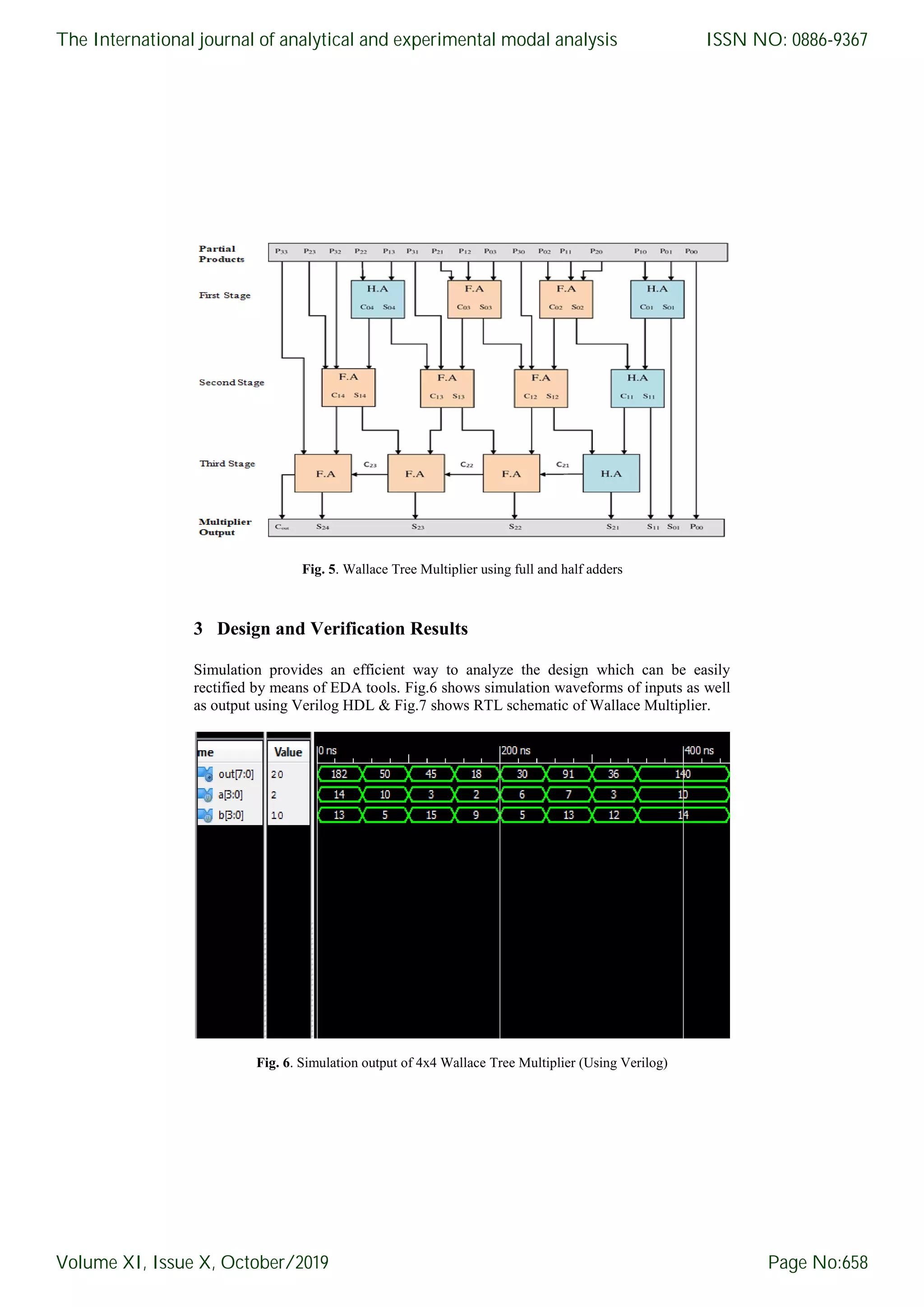
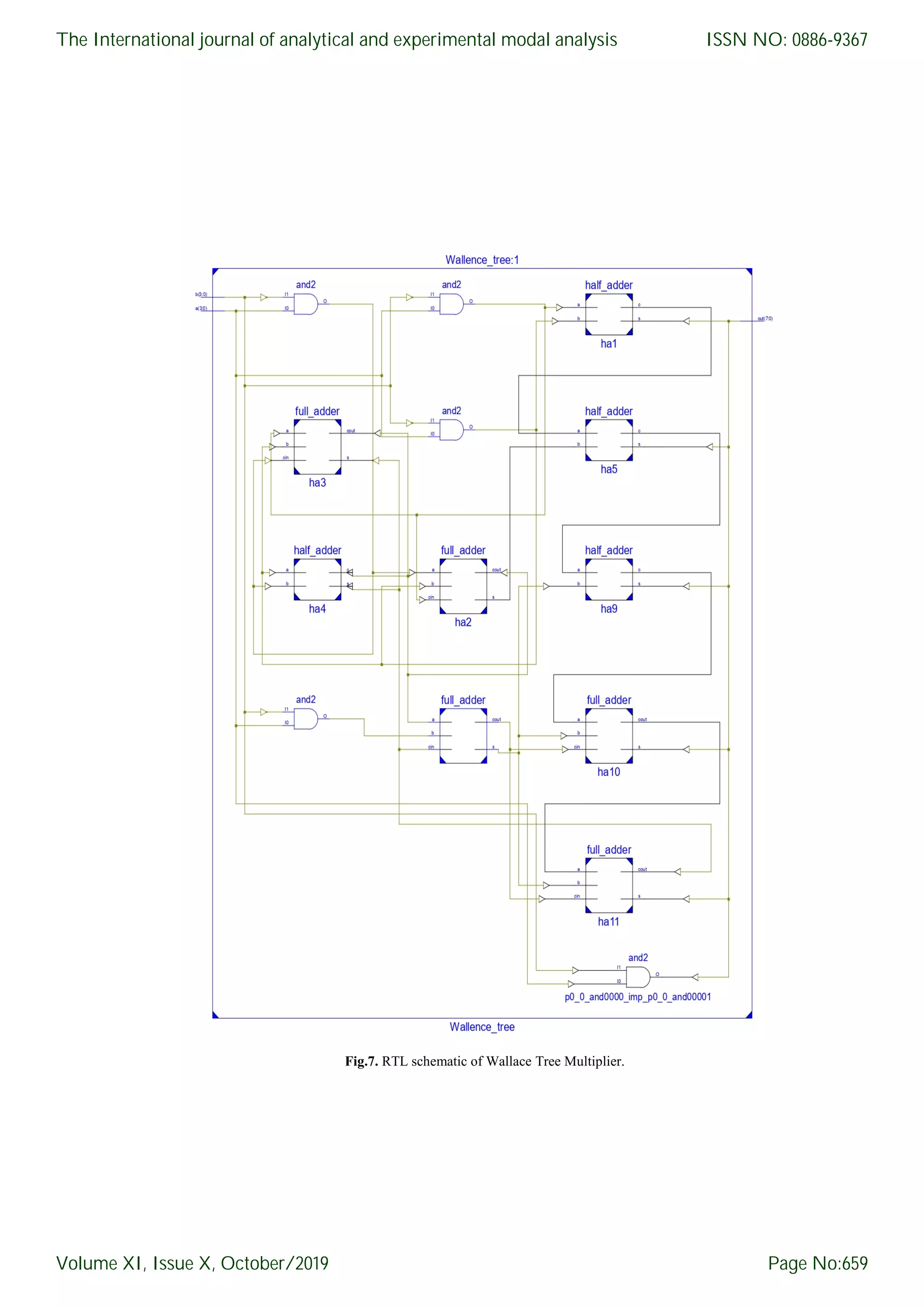
2 Wallace Tree Multiplier
The initial step is the formation of partial products by multiplying each bit from the
multiplier to same bit position of multiplicand. Secondly, groups of three adjacent
rows are collected. Each group of three rows is reduced by using half adders and full
adders.
Fig. 3. Operation of 4x4 Wallace Tree Multiplier
Half adders are used in each column where there are two bits whereas full adders are
used in each column where there are three bits, any single bit in column is passed to
next stage in the same column without any operation. This reduction procedure is
repeated in each successive stage until only two rows remain. In the final stage, the
remaining two rows are added. After completing all the three stages we get 8 bit of
output as shown in fig.5.
Fig.4.Block diagram of Wallace Tree Multiplier
The International journal of analytical and experimental modal analysis
Volume XI, Issue X, October/2019
ISSN NO: 0886-9367
Page No:657](https://image.slidesharecdn.com/72-october-2591-200321062623/75/Design-and-Verification-of-4-X-4-Wallace-Tree-Multiplier-3-2048.jpg)
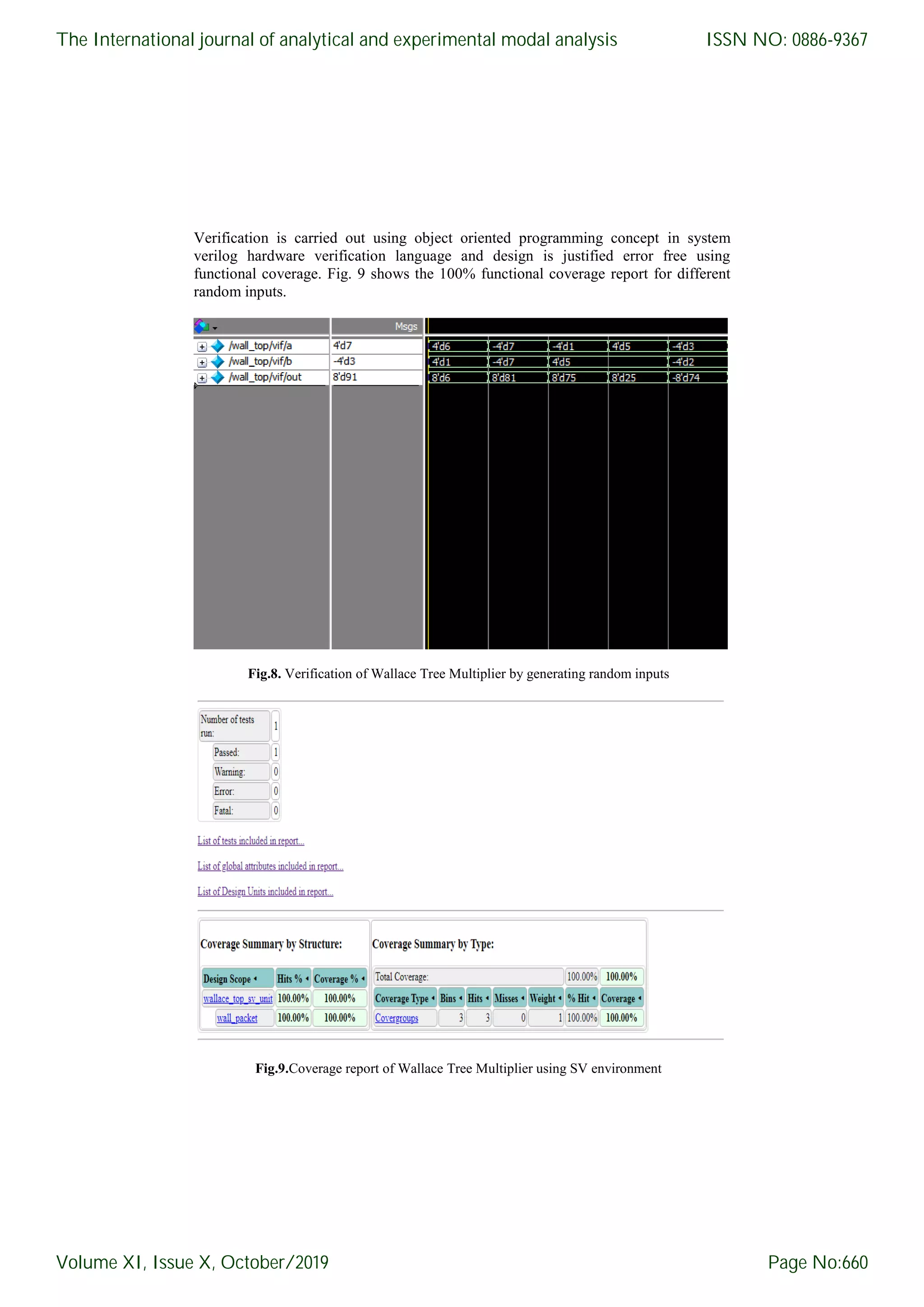

This paper studies the design and verification of a 4x4 Wallace tree multiplier, which is a high-speed and area-efficient hardware implementation for multiplying binary numbers. The design is created using Verilog HDL and verified using System Verilog HVL, achieving 100% functional coverage through extensive simulations. The work highlights the importance of multipliers in digital signal processing and demonstrates a rigorous approach to verifying digital circuit designs.