High –Speed Implementation of Design and Analysis by Using Parallel Prefix Ad...IOSRJECE
The binary adder is the critical element in most digital circuit designs including the digital signal processors (DSP) and microprocessor data unit path. As such as extensive research continues to be focused on improving the power, delay, improvement of the adder. The design and analysis of the parallel prefix adders (carry select adders) is to be implemented by using Verilog. In VLSI implementations, parallel prefix adders are very high speed performance. Binary adders are one of the most essential logic elements within a digital system. Therefore, binary addition is essential that any improvement in binary addition can result in a performance boost for any computing system and hence, help improve the performance of the entire system. Parallel-prefix adders (also known as carry-tree adders) are known to have the best performance in VLSI designs. This paper investigates (the Kogge-Stone, sparse Kogge-Stone, Ladner fischer adder, Brent-Kung adder) and compares them to the simple Ripple Carry Adder (RCA) for high number of binary bits.
An efficient model for design of 64-bit High Speed Parallel Prefix VLSI adderIJMER
International Journal of Modern Engineering Research (IJMER) is Peer reviewed, online Journal. It serves as an international archival forum of scholarly research related to engineering and science education.
International Journal of Engineering Research and Applications (IJERA) is an open access online peer reviewed international journal that publishes research and review articles in the fields of Computer Science, Neural Networks, Electrical Engineering, Software Engineering, Information Technology, Mechanical Engineering, Chemical Engineering, Plastic Engineering, Food Technology, Textile Engineering, Nano Technology & science, Power Electronics, Electronics & Communication Engineering, Computational mathematics, Image processing, Civil Engineering, Structural Engineering, Environmental Engineering, VLSI Testing & Low Power VLSI Design etc.
DUAL FIELD DUAL CORE SECURE CRYPTOPROCESSOR ON FPGA PLATFORMVLSICS Design
This paper is devoted to the design of dual core crypto processor for executing both Prime field and binary field instructions. The proposed design is specifically optimized for Field programmable gate array (FPGA) platform. Combination of two different field (prime field GF(p) and Binary field GF(2m)) instructions execution is analysed.The design is implemented in Spartan 3E and virtex5. Both the performance results are compared. The implementation result shows the execution of parallelism using dual field instructions
International Journal of Computational Engineering Research(IJCER) is an intentional online Journal in English monthly publishing journal. This Journal publish original research work that contributes significantly to further the scientific knowledge in engineering and Technology.
High Speed Area Efficient 8-point FFT using Vedic MultiplierIJERA Editor
A high speed fast fourier transform (FFT) design by using three algorithm is presented in this paper. In algorithm 3, 4-bit Vedic multiplier based technique are used in FFT. In this technique used in three 4-bit ripple carry adder and four 2*2 Vedic multiplier. The main parameter of this paper is number of slice, 4-input LUTS and maximum combinational path delay were calculate.
CFA based SBOX and Modified Mixcolumn Implementation of 8 Bit Datapath for AESidescitation
Secure data transmission is very important in any communication systems.
Network Security provides many techniques for efficient data transmission through
unprotected network. Cryptography provides a method for securing the transmission of
information by the process of encryption. Encryption converts the message in to unreadable
form (Cipher Text) . Decryption converts this Cipher Text back to original message.
Advanced Encryption Standard (AES) has been used as the first choice of cryptographic
algorithm for many security based applications because of the high level of security and
flexibility of implementation in hardware and software. This paper presents an area
efficient, low power design for AES based on an 8-bit data path making it suitable for
wireless security applications. It has a significant power-area-latency performance
improvements over other existing AES designs. For high performance applications, AES S-
box and inverse S-box implemented using composite field Arithmetic (CFA). Also low
resource Mixcolumn structure is used in this structure. The 8 bit data path architecture is
implemented in XILINX 13.2 and simulated using MODELSIM 6.5 software. Also the
power and area calculation is done with the help of SYNOPSYS software.
Implementation of an arithmetic logic using area efficient carry lookahead adderVLSICS Design
An arithmetic logic unit acts as the basic building blocks or cell of a central processing unit of a computer.
And it is a digital circuit comprised of the basic electronics components, which is used to perform various
function of arithmetic and logic and integral operations further the purpose of this work is to propose the
design of an 8-bit ALU which supports 4-bit multiplication. Thus, the functionalities of the ALU in this
study consist of following main functions like addition also subtraction, increment, decrement, AND, OR,
NOT, XOR, NOR also two complement generation Multiplication. And the functions with the adder in the
airthemetic logic unit are implemented using a Carry Look Ahead adder joined by a ripple carry approach.
The design of the following multiplier is achieved using the Booths Algorithm therefore the proposed ALU
can be designed by using verilog or VHDL and can also be designed on Cadence Virtuoso platform.
A study to Design and comparison of Full Adder using Various TechniquesIOSR Journals
Abstract: Adders is widely used in applications such as digital signal processing (DSP) and microprocessors. In this paper Half adders are simulated and analyzed based on power dissipation, area and speed on 90nm technology using Microwind and Dsch tool. Half Adder is the basic building block in Parallel Feedback Carry Adder (PFCA). Keywords: Full adder, Half adder, PFCA, VLSI
Braun’s Multiplier Implementation using FPGA with Bypassing Techniques.VLSICS Design
The developing an Application Specific Integrated Circuits (ASICs) will cost very high, the circuits should be proved and then it would be optimized before implementation. Multiplication which is the basic building block for several DSP processors, Image processing and many other. The Braun multipliers can easily be implemented using Field Programmable Gate Array (FPGA) devices. This research presented the comparative study of Spartan-3E, Virtex-4, Virtex-5 and Virtex-6 Low Power FPGA devices. The implementation of Braun multipliers and its bypassing techniques is done using Verilog HDL. We are proposing that adder block which we implemented our design (fast addition) and we compared the results of that so that our proposed method is effective when compare to the conventional design. There is the reduction in the resources like delay LUTs, number of slices used. Results are showed and it is verified using the Spartan-3E, Virtex-4 and Virtex-5 devices. The Virtex-5 FPGA has shown the good performance as compared to Spartan-3E and Virtex-4 FPGA devices.
International Journal of Engineering Research and Applications (IJERA) is an open access online peer reviewed international journal that publishes research and review articles in the fields of Computer Science, Neural Networks, Electrical Engineering, Software Engineering, Information Technology, Mechanical Engineering, Chemical Engineering, Plastic Engineering, Food Technology, Textile Engineering, Nano Technology & science, Power Electronics, Electronics & Communication Engineering, Computational mathematics, Image processing, Civil Engineering, Structural Engineering, Environmental Engineering, VLSI Testing & Low Power VLSI Design etc.
Low Power Parellel Chein Search Architecture using Two- Step ApproachMonalSarada
This brief proposes a new power-efficient Chien search (CS) architecture for parallel Bose-Chaudhuri-Hocquenghem (BCH) codes. In the proposed architecture, the searching process is decomposed into two steps based on the binary matrix representation. Unlike the first step accessed every cycle, the second step is activated only when the first step is successful, resulting in remarkable power saving.
A Novel VLSI Architecture for FFT Utilizing Proposed 4:2 & 7:2 CompressorIJERD Editor
With the appearance of new innovation in the fields of VLSI and correspondence, there is likewise a perpetually developing interest for fast transforming and low range outline. It is likewise a remarkable certainty that the multiplier unit structures a fundamental piece of processor configuration. Because of this respect, rapid multiplier architectures turn into the need of the day. In this paper, we acquaint a novel structural engineering with perform high velocity duplication utilizing old Vedic math's strategies. Another fast approach using 4:2 compressors and novel 7:2 compressors for expansion has additionally been joined in the same and has been investigated. Upon examination, the compressor based multiplier present in this paper, is just about two times quicker than the mainstream routines for augmentation. Likewise we outline a FFT utilizing compressor based multiplier. This all configuration and examinations were done on a Xilinx Spartan 3e arrangement of FPGA and the timing and zone of the outline, on the same have been ascertained.
Implementation and Design of High Speed FPGA-based Content Addressable Memoryijsrd.com
CAM stands for content addressable memory. It is a special type of computer memory used in very high speed searching application. A CAM is a memory that implements the high speed lookup-table function in a single clock cycle using dedicated comparison circuitry. It is also known as associative memory or associative array although the last term used for a programming data structure. Unlike standard computer memory (RAM) in which user supplies the memory address and the RAM returns the data word stored in that memory address, CAM is designed in such a way that user supplies data word and CAM searches its entire memory to see if that data word stored anywhere in it. If the data word is found, the CAM returns a list of one or more storage address where the word was found. This design coding, simulation, logic synthesis and implementation will be done using various EDA tools.
IOSR journal of VLSI and Signal Processing (IOSRJVSP) is a double blind peer reviewed International Journal that publishes articles which contribute new results in all areas of VLSI Design & Signal Processing. The goal of this journal is to bring together researchers and practitioners from academia and industry to focus on advanced VLSI Design & Signal Processing concepts and establishing new collaborations in these areas.
Design and realization of microelectronic systems using VLSI/ULSI technologies require close collaboration among scientists and engineers in the fields of systems architecture, logic and circuit design, chips and wafer fabrication, packaging, testing and systems applications. Generation of specifications, design and verification must be performed at all abstraction levels, including the system, register-transfer, logic, circuit, transistor and process levels
Introduction to CMOS VLSI Design:
This Presentations is design in way to provide basic summary of CMOS Vlsi design
This Presentation is Made at Eutectics.blogspot.in
the following is the structure of presentation :
2: Outline
3: Introduction
4: MOS capacitor
5: Terminal Voltage
6: nMOS Cutoff
7: nMOS Linear
8: nMOS Saturation
9: I-V Characteristics
10 : Channel Charge
11: Carrier velocity
12: nMOS Linear I-V
13: nMOS Saturation
14: nMOS I-V Summary
15: Example
16: pMOS I-V
17: Capacitance
18: Gate Capacitance
19: Diffusion Capacitane
20: Pass Transistor
21: Pass transistor ckts
22: Effective Resistance
23: RC Delay Model
24: RC values
25: Inverter Delay Estimate
Phytochemical, cytotoxic, in-vitro antioxidant and anti-microbial investigati...IOSR Journals
Zizyphus rugosa Lam. (Family: Rhamnaceae), locally known as “Bon Boroi” or as “Jongli Boroi” in Bangladesh generally found as a herb on the hills in bunches on thorny branches of the Zizyphus rugosa trees. Its bark and wood are used medicinally for dysentery in China, India, Laos, Burma, Sri Lanka, Thailand and Vietnam. Phytochemical screening of the Leaf extract of Zizyphus rugosa Lam showed different phytoconstituents including carbohydrates (monosaccharides, reducing and mixed-reducing sugars), alkaloid, glycosides, steroids, tannins and saponin. No flavonoid was detected. In DPPH and NO radical scavenging methods, IC50 was moderately satisfactory. IC50 was found 179.713μg/ml and 769.909μg/ml respectively compare with the reference ascorbic acid (15.707μg/ml and 82.642μg/ml respectively). In LPO (Lipid peroxidation) assay the Leaf fraction extract showed moderate inhibition potentiality (IC50 402.835μg/ml) in comparison to standard drug BHT (IC50 32.94μg/ml). In CUPRAC assays, the fraction was found to possess low Total antioxidant content, good flavonoid, and moderate amounts of phenolics, tannin and alkaloid content. The Leaf fraction extract was found to show good toxicity to Brine Shrimp nauplii, (LC50 212.402μg/ml & LC90 10715.91μg/ml) compare with the reference anticancer drug vincristine sulphate (LC50 2.47μg/ml & LC90 42μg/ml). In the antimicrobial study the fraction showed moderate activity against only one bacterium (Shiggla sonni) while the standard drug Chloramphenicol showed very good zone of inhibition against all five types (Salmonella typhi, Staphylococcus aureus, Shiggla sonni, Salmonella paratyphi, Salmonella grb) of bacteria. These findings provide scientific basis for the use of Zizyphus rugosa Lam. leaf ethanolic extract in traditional medicine in the treatment of aforementioned diseases. The plant also possesses moderate antimicrobial activity, good cytotoxic and good to moderate antioxidant activity.
Qualitative Chemistry Education: The Role of the TeacherIOSR Journals
Abstract: This paper discussed the role of a chemistry teacher towards improving the quality of education in Nigeria. The decline in the quality of education has been attributed to many factors. Some of these factors are unqualified teachers, examination malpractice,, lack of practical skills, method of classroom instruction, to mention but a few. The role of a chemistry teacher among others is to change the method of classroom instruction from lecture method to innovative learning strategy such as cooperative learning and concept mapping, and to make use of improvised materials in the absence of standard equipments . It also examine the problems associated with the fall in quality of education. Finally it is recommended that Government should ensure that adequate funds are released to train science teachers, since teachers are the main determinant of quality in Education.
Educational Process Mining-Different PerspectivesIOSR Journals
Process mining methods have in recent years enabled the development of more sophisticated Process
models which represent and detect a broader range of student behaviors than was previously possible. This
paper summarizes key Process mining perspectives that have supported student modeling efforts, discussing
also the specific constructs that have been modeled with the use of educational process mining and key
upcoming directions that are needed for educational process mining research to reach its full potential. Process
mining aims to discover, monitor and improve real processes by extracting knowledge from event logs readily
available in today’s information systems. This paper is designed to give a view on the capabilities of process
mining techniques in the context of higher education system which involves and deals with administrative and
academic tasks like enrolment of students in a particular case, alienation of traditional classroom teaching
model, detection of unfair means used in online examination, detection of abnormal values in the result sheet of
students, prediction about students performance, identify the drop outs, and students who need special attention
and allow the teacher to provide appropriate advising /counseling and so on.
(𝛕𝐢, 𝛕𝐣)− RGB Closed Sets in Bitopological SpacesIOSR Journals
In this paper we introduce and study the concept of a new class of closed sets called (𝜏𝑖, 𝜏𝑗)− regular generalized b- closed sets (briefly(𝜏𝑖, 𝜏𝑗)− rgb-closed) in bitopological spaces.Further we define and study new neighborhood namely (𝜏𝑖, 𝜏𝑗)− rgb- neighbourhood (briefly(𝜏𝑖, 𝜏𝑗)− rgb-nhd) and discuss some of their properties in bitopological spaces. Also, we give some characterizations and applications of it.
Spectrophotometric Determination of Drugs and Pharmaceuticals by Cerium (IV) ...IOSR Journals
Simple, sensitive, accurate, and precise spectrophotometric methods for quantitative determination of drugs, viz., Darifenacin (DAR), Esmolol Hydrochloride (ESM), Montelukast Sodium (MON), Sildenafil citrate (SIL),Terbinafine (TER) and Tramadol Hydrochloride (TRA) were developed. The method of each drug depends upon oxidation of drugs by Ce (IV) (Excess) and estimating the amount of unreacted Ce (IV) by amaranth dye at 523nm. The calibration curves obeyed Beer’s law over the concentration range of 1.4-7.0 μg ml-1 (DAR), 2-14 μg ml-1 (ESM), 2-10 μg ml-1 (MON), 20-70 μg ml-1 (SIL), 3-21 μg ml-1 (TER) & 2-14 μg ml-1 (TRA). The methods have been validated in terms of guidelines of ICH and applied to analysis of pharmaceuticals.
Area, Delay and Power Comparison of Adder TopologiesVLSICS Design
Adders form an almost obligatory component of every contemporary integrated circuit. The prerequisite of the adder is that it is primarily fast and secondarily efficient in terms of power consumption and chip area. This paper presents the pertinent choice for selecting the adder topology with the tradeoff between delay, power consumption and area. The adder topology used in this work are ripple carry adder, carry lookahead adder, carry skip adder, carry select adder, carry increment adder, carry save adder and carry bypass adder. The module functionality and performance issues like area, power dissipation and propagation delay are analyzed at 0.12µm 6metal layer CMOS technology using microwind tool.
Design Of 64-Bit Parallel Prefix VLSI Adder For High Speed Arithmetic CircuitsIJRES Journal
Parallel prefix adder is a kind of process for speeding up the addition of the system of writing and calculating with numbers which use only two digits. Parallel prefix adders are also known as carry-tree adders and they are known to have the best performance in VLSI designs. Due to constraints on logic blog configurations a routing overhead, this performance advantage does not translate directly into FPGA implementations. Identifying the absolutely accurate area-delay tradeoff curve of the parallel prefix is an interesting problem that has received more attention in research because parallel prefix adder on the other hand represents a type of general adder structure that displays publically in flexible area-time tradeoffs for the design of adder. Many different types of parallel prefix adders are made to increase for optimizing area, fan out, speed and performance. For high speed performance tree like structure is must which helps in greater way. There are many different method used for designing parallel prefix adder based on their speed, size and performance. For area optimization we use Brent-Kung method. If our main purpose is to get the least timing then we have to use Kogg-Stone adder method.
Design of 32 bit Parallel Prefix Adders IOSR Journals
In this paper, we propose 32 bit Kogge-Stone, Brent-Kung, Ladner-Fischer parallel prefix adders. In
general N-bit adders like Ripple Carry Adders (slow adders compare to other adders), and Carry Look Ahead
adders (area consuming adders) are used in earlier days. But now the most Industries are using parallel prefix
adders because of their advantages compare to other adders. Parallel prefix adders are faster and area
efficient. Parallel prefix adder is a technique for increasing the speed in DSP processor while performing
addition. We simulate and synthesis different types of 32-bit prefix adders using Xilinx ISE 10.1i tool. By using
these synthesis results, we noted the performance parameters like number of LUTs and delay. We compare these three adders in terms of LUTs (represents area) and delay values.
Design of 32 bit Parallel Prefix AddersIOSR Journals
Abstract: In this paper, we propose 32 bit Kogge-Stone, Brent-Kung, Ladner-Fischer parallel prefix adders. In general N-bit adders like Ripple Carry Adders (slow adders compare to other adders), and Carry Look Ahead adders (area consuming adders) are used in earlier days. But now the most Industries are using parallel prefix adders because of their advantages compare to other adders. Parallel prefix adders are faster and area efficient. Parallel prefix adder is a technique for increasing the speed in DSP processor while performing addition. We simulate and synthesis different types of 32-bit prefix adders using Xilinx ISE 10.1i tool. By using these synthesis results, we noted the performance parameters like number of LUTs and delay. We compare these three adders in terms of LUTs (represents area) and delay values. Keywords− prefix adder, carry operator, Kogge-Stone, Brent-Kung, Ladner-Fischer
International Journal of Engineering Research and Applications (IJERA) is an open access online peer reviewed international journal that publishes research and review articles in the fields of Computer Science, Neural Networks, Electrical Engineering, Software Engineering, Information Technology, Mechanical Engineering, Chemical Engineering, Plastic Engineering, Food Technology, Textile Engineering, Nano Technology & science, Power Electronics, Electronics & Communication Engineering, Computational mathematics, Image processing, Civil Engineering, Structural Engineering, Environmental Engineering, VLSI Testing & Low Power VLSI Design etc.
An Efficient High Speed Design of 16-Bit Sparse-Tree RSFQ AdderIJERA Editor
In this paper, we propse 16-bit sparse tree RSFQ adder (Rapid single flux quantam), kogge-stone adder, carry lookahead adder. In general N-bit adders like Ripple carry adder s(slow adders compare to other adders), and carry lookahead adders(area consuming adders) are used in earlier days. But now the most of industries are using parallel prefix adders because of their advantages compare to kogge-stone adder, carry lookahead adder, Our prefix sparse tree adders are faster and area efficient. Parallel prefix adder is a technique for increasing the speed in DSP processor while performing addition. We simulate and synthesis different types of 16-bit sparse tree RSFQ adders using Xilinx ISE10.1i tool, By using these synthesis results, We noted the performance parameters like number of LUT’s and delay. We compare these three adders interms of LUT’s represents area) and delay values.
Design of High Speed 128 bit Parallel Prefix AddersIJERA Editor
In this paper, we propose 128-bit Kogge-Stone, Ladner-Fischer, Spanning tree parallel prefix adders and
compared with Ripple carry adder. In general N-bit adders like Ripple Carry Adders (slow adders compare to
other adders), and Carry Look Ahead adders (area consuming adders) are used in earlier days. But now the most
Industries are using parallel prefix adders because of their advantages compare to other adders. Parallel prefix
adders are faster and area efficient. Parallel prefix adder is a technique for increasing the speed in DSP processor
while performing addition. While when we want to design any 128-bit operating systems and processors we can
use these adders in place of regular adders. We simulate and synthesis different types of 128-bit prefix adders
using Xilinx ISE 12.3 tool. By using these synthesis results, we noted the performance parameters like number
of LUTs and delay. We compare these three adders in terms of LUTs (represents area) and delay values.
Design and Estimation of delay, power and area for Parallel prefix addersIJERA Editor
In Very Large Scale Integration (VLSI) designs, Parallel prefix adders (PPA) have the better delay performance. This paper investigates four types of PPA’s (Kogge Stone Adder (KSA), Spanning Tree Adder (STA), Brent Kung Adder (BKA) and Sparse Kogge Stone Adder (SKA)). Additionally Ripple Carry Adder (RCA), Carry Look ahead Adder (CLA) and Carry Skip Adder (CSA) are also investigated. These adders are implemented in verilog Hardware Description Language (HDL) using Xilinx Integrated Software Environment (ISE) 13.2 Design Suite. These designs are implemented in Xilinx Spartan 6 Field Programmable Gate Arrays (FPGA). Delay and area are measured using XPower analyzer and all these adder’s delay, power and area are investigated and compared finally
128-Bit Area Efficient Reconfigurable Carry Select Adder ijcisjournal
Adders are one of the most critical arithmetic circuits in a system and their throughput affects the overall
performance of the system. Carry Select Adder (CSLA) is one of the fastest adders used in many dataprocessing
processors to perform fast arithmetic functions. From the structure of the CSLA, it is clear that
there is scope for reducing the area and power consumption in the CSLA. In this paper, we proposed an
area-efficient carry select adder by sharing the common Boolean logic term. After logic optimization and
sharing partial circuit, we only need one XOR gate and one inverter gate for sum generation. Through the
multiplexer, we can select the final-sum only and for carry selection we need only one AND gate and one
OR gate. Based on this modification 16-, 32-, 64-, and 128-bit CSLA architecture have been developed and
compared with the conventional CSLA architecture. The proposed design greatly reduces the area
compared to other CSLAs. From this improvement, the gate count of a 128-bit carry select adder can be
reduced from 3320 to 1664. The proposed structure is implemented in Artix-7 FPGA. Compared with the
proposed design, the conventional CSLA has 65.80% less area.
Design and implementation of Closed Loop Control of Three Phase Interleaved P...IJMTST Journal
A single-phase, three-level, single-stage power-factor corrected AC/DC converter operated under closed
loop manner is presented. That operates with a single controller to regulate the output voltage and the input
inductor act as a boost inductor to have a single stage power factor correction with good output response. The
paper deals with a new single stage three level ac-dc converter which performs both power factor correction
and voltage regulation in a single stage. The proposed converter has two separate controllers, one for power
factor correction and the other for regulating the output voltage. A comprehensive review of the existing single
stage topologies has been carried out. Then the operating principle, control scheme and the design of the new
converter are presented. The proposed converter is having an input power factor close to unity and better
voltage regulation compared to the conventional ac-dc converter topologies. Proposed topology is evaluated
through Matlab/Simulink platform and simulation results are conferred.
— Parallel Prefix adders have been one of the most
notable among several designs proposed in the past. The
advantage of utilizing the flexibility in implementing these
structures based upon through put requirements. Due to
continuing integrating intensity and the growing needs of
portable devices, low power and high performance designs are of
prime importance. The classical parallel prefix adder structures
presented in the literature over the years optimize for logic depth,
area, and fan-out and interconnect count of logic circuits. In this
proposed system, Kogge-Stone adder which is one of types of
parallel prefix adder is used. Kogge stone is the fastest adder
because of its minimum fan-out. When parallel prefix adder is
compared with classical adders it is advantageous in every aspect.
The study reveals that Parallel Prefix adder has the least power
delay product when compared with its peer existing adder
structures (Ripple carry adder, Carry save adders etc).
Simulation results are verified using Xilinx 10.1 and
MODELSIM 6.4a softwares.
International Journal of Engineering Research and Applications (IJERA) is an open access online peer reviewed international journal that publishes research and review articles in the fields of Computer Science, Neural Networks, Electrical Engineering, Software Engineering, Information Technology, Mechanical Engineering, Chemical Engineering, Plastic Engineering, Food Technology, Textile Engineering, Nano Technology & science, Power Electronics, Electronics & Communication Engineering, Computational mathematics, Image processing, Civil Engineering, Structural Engineering, Environmental Engineering, VLSI Testing & Low Power VLSI Design etc.
High Speed and Area Efficient Booth Multiplier Using SQRT CSLA with Zero Find...IJERA Editor
Addition is one of the common and widely used fundamental arithmetic operation in many VLSI systems. The critical elements in general purpose and digital-signal processing processors are High performance VLSI integer adders as they are employed in the design of Arithmetic-Logic Units, in floating-point arithmetic data paths and in address generation units. The performance parameters for any adder are area, speed and delay. By using Square Root Carry Select Adder (SQRT CSLA), speed can be achieved. In designing new architecture, the Tradeoff between those parameters plays the major role. We can reduce area by using Zero Finding Logic (ZFC) technique, from the structure of SQRT CSLA. By using the Modified architecture we can reduce area. We can implement Booth multiplier by using the CSLA and SQRT CSLA with Zero finding logic. Implementation of Booth multiplier by using CSLA and SQRT CSLA with Zero finding logic is proposed for better speed applications and efficient area applications.
International Journal of Engineering Research and Applications (IJERA) is an open access online peer reviewed international journal that publishes research and review articles in the fields of Computer Science, Neural Networks, Electrical Engineering, Software Engineering, Information Technology, Mechanical Engineering, Chemical Engineering, Plastic Engineering, Food Technology, Textile Engineering, Nano Technology & science, Power Electronics, Electronics & Communication Engineering, Computational mathematics, Image processing, Civil Engineering, Structural Engineering, Environmental Engineering, VLSI Testing & Low Power VLSI Design etc.
a technical review of efficient and high speed adders for vedic multipliersINFOGAIN PUBLICATION
n the VLSI system design, the main regions of research are the reduced size & increase speed path logic systems. A fundamental requirement of high speed, addition and multiplication is always needed for the high performance digital processors. In the digital system, the speed of addition depend on the propagation of carry, which is generated successively, after the previous bit has been summed & carry is propagated, into the next location. There are numerous types of adders available likes Ripple Carry Adder, Carry Look Ahead Adder, Carry Save Adder, Carry Avoid Adder, and Carry Select Adder, which have their own benefits and drawbacks. With the advances technology, proposal of Carry select adder (CSA) which deals either of the high speed, low power consumption, regularity of layout a smaller amount area and compact VLSI design implementation. Researchers justify that Ripple Carry Adder had a lesser area but having lesser in speed, in comparing with Carry Select Adders are fastest speed but possess a larger area. The Carry Look Ahead Adder is in between the spectrum having proper trade-offs between time and area complexities.
Final project report on grocery store management system..pdfKamal Acharya
In today’s fast-changing business environment, it’s extremely important to be able to respond to client needs in the most effective and timely manner. If your customers wish to see your business online and have instant access to your products or services.
Online Grocery Store is an e-commerce website, which retails various grocery products. This project allows viewing various products available enables registered users to purchase desired products instantly using Paytm, UPI payment processor (Instant Pay) and also can place order by using Cash on Delivery (Pay Later) option. This project provides an easy access to Administrators and Managers to view orders placed using Pay Later and Instant Pay options.
In order to develop an e-commerce website, a number of Technologies must be studied and understood. These include multi-tiered architecture, server and client-side scripting techniques, implementation technologies, programming language (such as PHP, HTML, CSS, JavaScript) and MySQL relational databases. This is a project with the objective to develop a basic website where a consumer is provided with a shopping cart website and also to know about the technologies used to develop such a website.
This document will discuss each of the underlying technologies to create and implement an e- commerce website.
Explore the innovative world of trenchless pipe repair with our comprehensive guide, "The Benefits and Techniques of Trenchless Pipe Repair." This document delves into the modern methods of repairing underground pipes without the need for extensive excavation, highlighting the numerous advantages and the latest techniques used in the industry.
Learn about the cost savings, reduced environmental impact, and minimal disruption associated with trenchless technology. Discover detailed explanations of popular techniques such as pipe bursting, cured-in-place pipe (CIPP) lining, and directional drilling. Understand how these methods can be applied to various types of infrastructure, from residential plumbing to large-scale municipal systems.
Ideal for homeowners, contractors, engineers, and anyone interested in modern plumbing solutions, this guide provides valuable insights into why trenchless pipe repair is becoming the preferred choice for pipe rehabilitation. Stay informed about the latest advancements and best practices in the field.
Industrial Training at Shahjalal Fertilizer Company Limited (SFCL)MdTanvirMahtab2
This presentation is about the working procedure of Shahjalal Fertilizer Company Limited (SFCL). A Govt. owned Company of Bangladesh Chemical Industries Corporation under Ministry of Industries.
Water scarcity is the lack of fresh water resources to meet the standard water demand. There are two type of water scarcity. One is physical. The other is economic water scarcity.
Cosmetic shop management system project report.pdfKamal Acharya
Buying new cosmetic products is difficult. It can even be scary for those who have sensitive skin and are prone to skin trouble. The information needed to alleviate this problem is on the back of each product, but it's thought to interpret those ingredient lists unless you have a background in chemistry.
Instead of buying and hoping for the best, we can use data science to help us predict which products may be good fits for us. It includes various function programs to do the above mentioned tasks.
Data file handling has been effectively used in the program.
The automated cosmetic shop management system should deal with the automation of general workflow and administration process of the shop. The main processes of the system focus on customer's request where the system is able to search the most appropriate products and deliver it to the customers. It should help the employees to quickly identify the list of cosmetic product that have reached the minimum quantity and also keep a track of expired date for each cosmetic product. It should help the employees to find the rack number in which the product is placed.It is also Faster and more efficient way.
Student information management system project report ii.pdfKamal Acharya
Our project explains about the student management. This project mainly explains the various actions related to student details. This project shows some ease in adding, editing and deleting the student details. It also provides a less time consuming process for viewing, adding, editing and deleting the marks of the students.
Student information management system project report ii.pdf
Evaluation of High Speed and Low Memory Parallel Prefix Adders
1. IOSR Journal of Electrical and Electronics Engineering (IOSR-JEEE)
e-ISSN: 2278-1676,p-ISSN: 2320-3331, Volume 8, Issue 4 (Nov. - Dec. 2013), PP 13-20
www.iosrjournals.org
www.iosrjournals.org 13 | Page
Evaluation of High Speed and Low Memory Parallel Prefix
Adders
*
A.Madhu Babu1
, K.Harikrishna2
1
PG Student (M. Tech), Dept. of ECE, Chirala Engineering College, Chirala., A.P, India.
2
Associate Professor, Dept. of ECE, Chirala Engineering College, Chirala., A.P, India.
Abstract: The binary adder is the critical element in most digital circuit designs including digital signal
processors (DSP) and microprocessor data path units. As such, extensive research continues to be focused on
improving the power delay performance of the adder. In VLSI implementations, parallel-prefix adders are
known to have the best performance. Parallel-prefix adders (also known as carry-tree adders) are known to
have the best performance in VLSI designs. This paper investigates three types of carry-tree adders (the Kogge-
Stone, sparse Kogge-Stone, and spanning tree adder) and compares them to the simple Ripple Carry Adder
(RCA). In this project Xilinx-ISE tool is used for simulation, logical verification, and further synthesizing .
Keywords: DSP, Adders, Delay, Power.
I. Introduction
Arithmetic is the oldest and most elementary branch of Mathematics. The name Arithmetic comes from
the Greek word άριθμός (arithmos). Arithmetic is used by almost everyone, for tasks ranging from simple day to
day work like counting to advanced science and business calculations. As a result, the need for faster and
efficient Adders in computers has been a topic of interest over decades. Addition is a fundamental operation for
any digital system, digital signal processing or control system. A fast and accurate operation of a digital system is
greatly influenced by the performance of the resident adders. Adders are also very important component in digital
systems because of their extensive use in other basic digital operations such as subtraction, multiplication and
division. Hence, improving performance of the digital adder would greatly advance the execution of binary
operations inside a circuit compromised of such blocks. The performance of a digital circuit block is gauged by
analyzing its power dissipation, layout area and its operating speed.
To humans, decimal numbers are easy to comprehend and implement for performing arithmetic. However,
in digital systems, such as a microprocessor, DSP (Digital Signal Processor) or ASIC (Application-Specific
Integrated Circuit), binary numbers are more pragmatic for a given computation. This occurs because binary
values are optimally efficient at representing many values.
Binary adders are one of the most essential logic elements within a digital system. In addition, binary
adders are also helpful in units other than Arithmetic Logic Units (ALU), such as multipliers, dividers and
memory addressing. Therefore, binary addition is essential that any improvement in binary addition can result in
a performance boost for any computing system and, hence, help improve the performance of the entire system.
The major problem for binary addition is the carry chain. As the width of the input operand increases, the length
of the carry chain increases. Figure 1 demonstrates an example of an 8- bit binary add operation and how the
carry chain is affected. This example shows that the worst case occurs when the carry travels the longest
possible path, from the least significant bit (LSB) to the most significant bit (MSB). In order to improve the
performance of carry-propagate adders, it is possible to accelerate the carry chain, but not eliminate it.
Consequently, most digital designers often resort to building faster adders when optimizing computer
architecture, because they tend to set the critical path for most computations.
Figure 1 Binary Adder Example.
2. Evaluation Of High Speed And Low Memory Parallel Prefix Adders
www.iosrjournals.org 14 | Page
II. REVIEW Of ADDERS
FULL ADDER
A Full Adder is a combinational circuit that performs the arithmetic sum of three input bits. It consists of
three inputs and two outputs. Three of the input variables can be defined as A, B, Cin and the two output
variables can be defined as S, Cout. The two input variables that we defined earlier A and B represents the two
significant bits to be added. The third input Cin represents the carry bit. We have to use two digits because the
arithmetic sum of the three binary digits needs two digits. The two outputs represents S for sum and Cout for
carry. For designing a full adder circuit, two half adder circuits and an OR gate is required. It is the simplest way
to design a full adder circuit. To design a full adder two XOR gates, two AND gates, one OR gate is required
Figure 2 Full adder structure
S = A ^ B ^ C
cout = A.B + (A ^ B).Cin
PROPOGATION DELAY IN FULL ADDERS
Real logic gates do not react instantaneously to the inputs, and therefore digital circuits have a maximum
speed. Usually, the delay through a digital circuit is measured in gate-delays, as this allows the delay of a design
to be calculated for different devices. AND and OR gates have a nominal delay of 1 gate-delay, and XOR gates
have a delay of 2, because they are really made up of a combination of ANDs and ORs.
A full adder block has the following worst case propagation delays:
o From Ai or Bi to Ci+1: 4 gate-delays (XOR → AND → OR)
o From Ai or Bi to Si: 4 gate-delays (XOR → XOR)
o From Ci to Ci+1: 2 gate-delays (AND → OR)
o From Ci to Si: 2 gate-delays (XOR)
Because the carry-out of one stage is the next's input, the worst case propagation delay is then:
o 4 gate-delays from generating the first carry signal (A0/B0 → C1).
o 2 gate-delays per intermediate stage (Ci → Ci+1).
o 2 gate-delays at the last stage to produce both the sum and carry-out outputs (Cn1 → Cn and Sn-1).
So for an n-bit adder, we have a total propagation delay, tp of:
tp = 4+2(n-2)+2 = 2n+2
Figure 3 Delay in a full adder
This is linear in n, and for a 32-bit number, would take 66 cycles to complete the calculation. This is
somewhat rather slow, and restricts the word length in our device We would like to find ways to speed it up.
CARRY – LOOK AHEAD ADDER
A fast method of adding numbers is called carry-look ahead adder. This method doesn't require the carry
signal to propagate stage by stage, causing a bottleneck. Instead it uses additional logic to expedite the
propagation and generation of carry information, allowing fast addition at the expense of more hardware
requirements. Rather than waiting for carry signals to ripple from the least significant to the most significant bit,
CLA adders divided the inputs into groups of r bits and implement the logic equations to determine if each
group will generate or propagate carry.
3. Evaluation Of High Speed And Low Memory Parallel Prefix Adders
www.iosrjournals.org 15 | Page
An overview of the adder’s 4 stages is shown in the figure 2.5 with stage 1 and the top and stage 4 at the
bottom. In stage 1 the local generate and propagate signals for each bit are created. In stage 2 these signals are
combined into 9 bit block signals. In stage 4 the carry into each block is calculated and these signals begin
traveling back up the adder tree. In stage 3 the carry into local carry signals to calculate the final sum bits. Each
group is created, and into each bit is created. Finally, stage 1 uses the propogate and generates blocks to give the
sum as the output. The carry look ahead shows good performance for the lower order bits that is it shows better
performance for sum of less number of bits. The 32-bit carry look ahead adder shows better performance than
64-bit carry look ahead adder. Even the 64-bit adder shows better performance than 128 bit adder. As the bit
size increases the performance decreases in the carry look ahead adder.
Figure 4 Simple Adder Tree Structure
III. Parallel Prefix Adders
Parallel prefix adders employs 3- stage structure of carry look ahead adder The improvement is in the
carry generation stage which is the most intensive one. The below figure shows the structure of ling adder. The
ling adder uses predetermined propagates and generate in 1st
stage of design. The 2nd
stage uses the carry
calculation paralleled to reduce time .the 3rd
stage is the simple adder block to calculate the sum
Figure 5 Structure of the parallel prefix adder
Figure 6 Buffer & Processing component structure
The parallel prefix graph for representation of prefix addition is shown as
4. Evaluation Of High Speed And Low Memory Parallel Prefix Adders
www.iosrjournals.org 16 | Page
Figure 7 Parallel prefix adder structure
Some of the parallel prefix adders are :
Kogge-Stone adder
Sparse kogge stone adder
Spanning carry lookahead adder
Kogge stone adder
The Kogge–Stone adder is a parallel prefix form carry look-ahead adder. It generates the carry signals
in O(log n) time, and is widely considered the fastest adder design possible. It is the common design for high-
performance adders in industry.
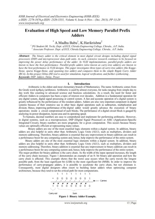
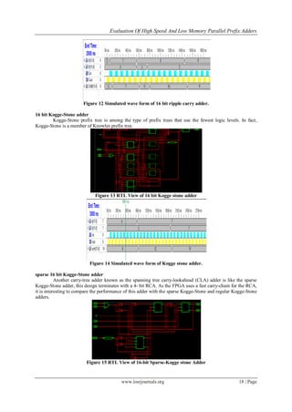
Kogge-Stone prefix tree is among the type of prefix trees that use the fewest logic levels. A 16-bit
example is shown in Figure 2.11. In fact, Kogge-Stone is a member of Knowles prefix tree. The 16-bit prefix
tree can be viewed as Knowles [1,1,1,1]. The numbers in the brackets represent the maximum branch fan-out at
each logic level. The maximum fan-out is 2 in all logic levels for all width Kogge-Stone prefix trees.
The key of building a prefix tree is how to implement Equation according to the specific features of
that type of prefix tree and apply the rules described in the previous section. Gray cells are inserted similar to
black cells except that the gray cells final output carry outs instead of intermediate G/P group. The reason of
starting with Kogge-Stone prefix tree is that it is the easiest to build in terms of using a program concept. The
example in Figure 8 is 16-bit (a power of 2) prefix tree. It is not difficult to extend the structure to any width if
the basics are strictly followed.
Figure 8 A 16-bit Kogge-Stone Prefix Tree
For the Kogge-Stone prefix tree, at the logic level 1, the inputs span is 1 bit (e.g. group (4:3) take the
inputs at bit 4 and bit 3). Group (4:3) will be taken as inputs and combined with group (6:5) to generate group
(6:3) at logic level 2. Group (6:3) will be taken as inputs and combined with group (10:7) to generate group
(10:3) at logic level 3, and so on so forth.
Sparse Kogge Stone Adder
The sparse Kogge-Stone adder consists of several smaller ripple carry adders (RCAs) on its lower half,
a carry tree on its upper half. It terminates with RCAs. The number of carries generated is less in a sparse
KoggeStone adder compared to the regular Kogge-Stone adder. The functionality of the GP block, black cell
and the gray cell remains exactly the same as in the regular Kogge-Stone adder. The sparse Kogge-Stone adder,
this design terminates with a 4- bit RCA. As the FPGA uses a fast carry-chain for the RCA, it is interesting to
compare the performance of this adder with the sparse Kogge-Stone and regular Kogge-Stone adders.
5. Evaluation Of High Speed And Low Memory Parallel Prefix Adders
www.iosrjournals.org 17 | Page
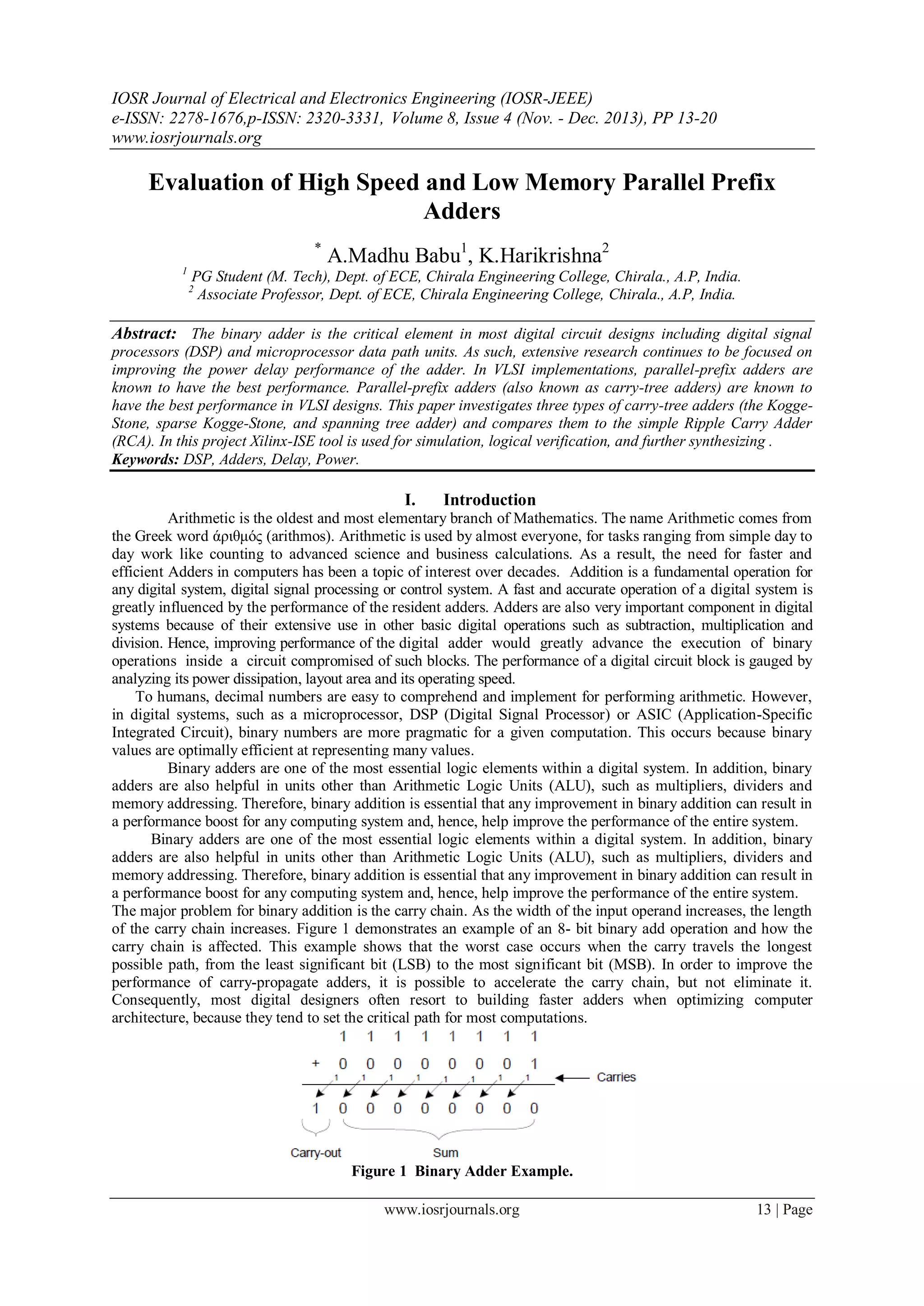
Spanning carry look ahead adder
Another carry-tree adder known as the spanning tree carry-lookahead (CLA) adder is like the sparse
Kogge-Stone adder, this design terminates with a 4- bit RCA. As the FPGA uses a fast carry-chain for the RCA,
it is interesting to compare the performance of this adder with the sparse Kogge-Stone and regular Kogge-Stone
adders.
Figure 10 16 bit Spanning tree carry look ahead adder
BINARY ADDER SCHEMES
Adders are one of the most essential components in digital building blocks, however, the performance
of adders become more critical as the technology advances. The problem of addition involves algorithms in
Boolean algebra and their respective circuit implementation. Algorithmically, there are linear-delay adders like
ripple-carry adders (RCA), which are the most straightforward but slowest. Adders like carry-skip adders
(CSKA), carry-select adders (CSEA) and carry-increment adders (CINA) are linear-based adders with optimized
carry-chain and improve upon the linear chain within a ripple-carry adder. Carry-lookahead adders (CLA) have
logarithmic delay and currently have evolved to parallel-prefix structures. Other schemes, like Ling adders,
NAND/NOR adders and carry-save adders can help improve performance as well.
IV. Simulation Results
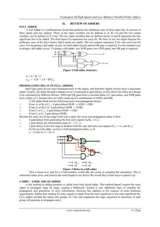
RIPPLE CARRY ADDER
The simplest way of doing binary addition is to connect the carry-out from the previous bit to the next
bit's carry-in. Each bit takes carry-in as one of the inputs and outputs sum and carry-out bit and hence the name
ripple-carry adder.
Figure 11 RTL view of 16 bit Ripple carry adder.
Figure 9 Block diagram of 16-Bit Sparse Kogge-Stone Adder[16].
6. Evaluation Of High Speed And Low Memory Parallel Prefix Adders
www.iosrjournals.org 18 | Page
Figure 12 Simulated wave form of 16 bit ripple carry adder.
16 bit Kogge-Stone adder
Kogge-Stone prefix tree is among the type of prefix trees that use the fewest logic levels. In fact,
Kogge-Stone is a member of Knowles prefix tree.
Figure 13 RTL View of 16 bit Kogge stone adder
Figure 14 Simulated wave form of Kogge stone adder.
sparse 16 bit Kogge-Stone adder
Another carry-tree adder known as the spanning tree carry-lookahead (CLA) adder is like the sparse
Kogge-Stone adder, this design terminates with a 4- bit RCA. As the FPGA uses a fast carry-chain for the RCA,
it is interesting to compare the performance of this adder with the sparse Kogge-Stone and regular Kogge-Stone
adders.
Figure 15 RTL View of 16-bit Sparse-Kogge stone Adder
7. Evaluation Of High Speed And Low Memory Parallel Prefix Adders
www.iosrjournals.org 19 | Page
Figure 16 Simulated wave form of 16 bit sparse-Kogge stone adder
16-bit Spanning Tree Carry Look ahead Adder
Another carry-tree adder known as the spanning tree carry-lookahead (CLA) adder is like the sparse
Kogge-Stone adder, this design terminates with a 4- bit RCA. As the FPGA uses a fast carry-chain for the RCA,
it is interesting to compare the performance of this adder with the sparse Kogge-Stone and regular Kogge-Stone
adders.
Figure 17 RTL View of 16-bit Spanning Tree Carry Look ahead Adder
Figure 18 Simulated waveform of 16 bit spanning carry look head adder.
Performance Comparative Analysis
The below comparison table is drawn from the analysis of four adders in terms of delay,memory and LUT’s
drawn from synthesis report.
Table 1 Comparison briefs of simulated adders
ADDER NAME Memory(KB) Delay(ns) LUT’S
KOGGE STONE 186972 25.084 36
SPARSE KOGGE STONE 187036 19.502 51
SPANNING TREE 186716 28.050 32
RIPPLE CARRY ADDER 189372 31.947 38
V. Conclusion:
The Adders namely ripple carry adder, Kogge stone adder , sparse Kogge stone adder and spanning tree
adder are discussed in detail. VERILOG code was written for all the modules. Each individual modules was
tested for its correct functionality.This project has resulted in the development of Adders Design with reduced
delay and memory advantage. The Delay measurement and memory analysis of the adders is being done.
8. Evaluation Of High Speed And Low Memory Parallel Prefix Adders
www.iosrjournals.org 20 | Page
From synthesis report the adders designed kogge stone adder , sparse kogge stone adder and spanning tree
adder is being compared with the normal ripple carry adder in terms of delay and memory. From the synthesis
report the delay is less for SPARSE KOGGE STONE adder and the memory is less for SPANNING TREE is
concluded. In future all the proposed architectures are designed using parallel prefix adders are used in the
design of MAC unit.
Acknowledgements
The authors would like to thank the anonymous reviewers for their comments which were very helpful
in improving the quality and presentation of this paper.
References
[1] B. Ramkumar and Harish M Kittur , ― Low-Power and Area-Efficient Carry Select Adder ―, IEEE Transactions on very large scale
integration (VLSI) systems, vol.20, no.2,pp.371-375, Feb .2012
[2] Dilip P. vasudevan, parag k.lala, james patrik parkerson, ― Self- checking carry-select adder design based on two rail en-coding‖,IEEE
Trans, CIRCUITS AND SYSTEMS—I , December 2007
[3] http://en.wikibooks.org/wiki/Digital_Circuits/Adders.html
[4] Yu-Ting Pai and Yu-Kumg Chen, ―The fastest carry look ahead adder,‖ IEEE trans . International Workshop on Electronic Design,
Test and Applications,vol.22. Feb .2004
[5] http://umunhum.stanford.edu /farland/notes.html
[6] Dayu Wang, Xiaoping Cui, Xiaojing Wang, ―Optimized design of Parallel Prefix Ling Adder,‖IEEE Trans. pp.941-944, oct.2011
[7] B.Bhaskar, M.Kanagasabapathy, V.S.Kanchana Bhaaskaran, ―A hybrid adiabatic parllel prefix addition scheme for low power‖, IEEE
Trans , International Conference on Recent Trends in Information Technology, pp.389-393 , june 2011
[8] G. W. Hanson, Fundamentals of Nanoelectronics. Englewood Cliffs,NJ: Prentice-Hall, 2008.
[9] R. Zhang, K. Walus, W. Wang, and G. A. Jullien, ―Performance comparisonof quantum-dot cellular automata adders,‖ in Proc. IEEE
Int. Symp.Circuits Syst., 2005, pp. 2522–2526.
[10] Architecture of FPGAs and CPLDs: A Tutorial - Computer ...www.eecg.toronto.edu/~jayar/pubs/brown/survey.pdfFile Format:
PDF/Adobe Acrobat - Quick View.
Authors Profile:
A. Madhu Babu is Pursuing his M. Tech from Chirala Engineering College, Chirala in the
department of Electronics & Communications En-gineering (ECE) with specialization in VLSI
& Embedded systems.
K. Hari Krishna is working as an Associate Professor in the department of Electronics &
Communication Engin-eering in Chirala Engineering College, Chirala. She completed masters
from JNTUK. She has over 8 years of teaching and two years industrial experience.