Downloaded 13 times
![Avneesh Kumar Mishra Int. Journal of Engineering Research and Applications www.ijera.com
ISSN : 2248-9622, Vol. 4, Issue 12( Part 4), December 2014, pp.105-108
www.ijera.com 105 | P a g e
High Speed Area Efficient 8-point FFT using Vedic Multiplier
Avneesh Kumar Mishra, Paresh Rawat,
Dept. of Electronics Communication, Truba College of Science and Technology, Bhopal, India
Abstract
A high speed fast fourier transform (FFT) design by using three algorithm is presented in this paper. In
algorithm 3, 4-bit Vedic multiplier based technique are used in FFT. In this technique used in three 4-bit ripple
carry adder and four 2*2 Vedic multiplier. The main parameter of this paper is number of slice, 4-input LUTS
and maximum combinational path delay were calculate.
Index Terms—FFT, Ripple Carry Adder, Carry Select Adder, Vedic Multiplier
I. INTRODUCTION
Digital signal processing (DSP) is the
mathematical manipulation of an information signal
to modify or improve it in some way. It is
characterized by the representation of discrete time,
discrete frequency, or other discrete domain signals
by a sequence of numbers or symbols and the
processing of these signals [1].
The goal of DSP is usually to measure, filter and/or
compress continuous real-world analog signals. The
first step is usually to convert the signal from an
analog to a digital form, by sampling and then
digitizing it using an analog-to-digital converter
(ADC), which turns the analog signal into a stream of
numbers. However, often, the required output signal
is another analog output signal, which requires a
digital-to-analog converter (DAC). Even if this
process is more complex than analog processing and
has a discrete value range, the application of
computational power to digital signal processing
allows for many advantages over analog processing
in many applications, such as error detection and
correction in transmission as well as data
compression. DSP algorithms have long been run on
standard computers, as well as on specialized
processors called digital signal processor and on
purpose-built hardware such as application-specific
integrated circuit (ASICs). Today there are additional
technologies used for digital signal processing
including more powerful general purpose
microprocessors, field-programmable gate arrays
(FPGAs), digital signal controllers (mostly for
industrial apps such as motor control), and stream
processors, among others [2-3]. The FFT is one of
the most commonly used digital signal processing
algorithm. Recently, FFT processor has been widely
used in digital signal processing field applied for
OFDM, MIMO-OFDM communication systems.
FFT/IFFT processors are key components for an
orthogonal frequency division multiplexing (OFDM)
based wireless IEEE 802.16 broadband
communication system; it is one of the most complex
and intensive computation module of various
wireless standards physical layer (ofdm-802.11a,
MIMO-OFDM 802.11, 802.16,802.16e) [4].
However, the main constraints nowadays for FFT
processors used in WiMAX and wireless
communication systems are execution time and lower
power consumption [5]. The main issue in FFT/IFFT
processors is complex and large multiplication, which
is the most addition and sub tractor arithmetic
operation used in FFT/IFFT blocks. It is an
expensive operation and consumes a large chip area
and power especially when it comes to a large FFT
point [6].
The speed of a processor depends on its multiplier’s
performance. This in turn increases the demand for
high speed and low power multipliers, at the same
time keeping in mind low area and moderate power
consumption [6].
Over the past few decades, several new structures of
multipliers have been designed and explored.
Multipliers based on the booth’s Algorithm [7], adder
and shift [7], ROM based multiplier, and modified
booth’s algorithm [8] is quite popular in modern
VLSI design but come along with their own set of
disadvantages. In these algorithms, the multiplication
process, involves several intermediate operations
before arriving at the final output.
In this paper design the 4-bit Vedic multiplier using
different adder and implementation 8-bit radix-2 FFT
algorithm.
The paper is organized as follows: Section II
discusses the FFT algorithm implementation radix-2
and complex multiplication used inside the butterfly-
processing element. Section III devoted for an
architectural description of the 4-bitadder used
module. Section IV shows the proposed three
algorithms. Section V shows the resulting
implementation and finally a conclusion is given in
section V.
RESEARCH ARTICLE OPEN ACCESS](https://image.slidesharecdn.com/q041204105108-150115052013-conversion-gate02/85/High-Speed-Area-Efficient-8-point-FFT-using-Vedic-Multiplier-1-320.jpg)
![Avneesh Kumar Mishra Int. Journal of Engineering Research and Applications www.ijera.com
ISSN : 2248-9622, Vol. 4, Issue 12( Part 4), December 2014, pp.105-108
www.ijera.com 108 | P a g e
Table 1: Synthesis Result for FFT Algorithm 1,
Algorithm 2 and Algorithm
Architecture Number of
slice
Number of
4-input
LUTs
Maximum
combination
al path delay
Algorithm 1 128 207 18.375 nsec
Algorithm 2 112 196 16.587 nsec
Algorithm 3 104 185 14.355 nsec
VI. CONCLUSION
A 4-bit adder, 4-bit ripple carry adder, 2*2 Vedic
multiplier, 4-bit binary multiplier, 4-bit multiplier
using 4-bit adder and 4-bit multiplier using ripple
carry adder have been proposed in this paper and
implementation in 8-point FFT. It is seen that the
speed of the algorithm 3 is higher than that of normal
array multiplier and multiplier using 4-bit adder. This
multiplier can be used in applications such as digital
signal processing, encryption and decryption
algorithms in cryptography.
ACKNOWLEDGMENT
REFERENCES
[1] Akhalesh K. Itawadiya, Rajesh Mahle, Vivek
Patel, Dadan Kumar, “Design a DSP
Operations using Vedic Mathematics”,
International conference on Communication
and Signal Processing, April 3-5, 2013, India.
[2] Sushma R. Huddar and Sudhir Rao, Kalpana
M., Surabhi Mohan, “Novel High Speed
Vedic Mathematics Multiplier using
Compressors”, 978-1-4673-5090-7/13/$31.00
©2013 IEEE.
[3] S. S. Kerur, Prakash Narchi, Jayashree C N,
Harish M Kittur and Girish V A,
“Implementation of Vedic multiplier for
Digital Signal Processing”, International
Conference on VLSI, Communication &
Instrumentation (ICVCI) 2011, Proceedings
published by International Joural of Computer
Applications® (IJCA), pp.1-6.
[4] Himanshu Thapaliyal and M.B Srinivas,
“VLSI Implementation of RSA Encryption
System Using Ancient Indian Vedic
Mathematics”, Center for VLSI and
Embedded System Technologies,
International Institute of Information
Technology Hyderabad, India.
[5] Jagadguru Swami Sri Bharati Krishna Tirthaji
Maharaja, “Vedic Mathematics: Sixteen
simple Mathematical Formulae from the
Veda”, Delhi(2011).
[6] Harpreet Singh Dhillon and Abhijit Mitra, “ A
Reduced-bit Multiplication Algorithm for
Digital Arithmetic”, International Journal of
Computational and Mathematical Sciences,
Febrauary 2008, pp.64-69.
[7] Sumit Vaidya and Depak Dandekar. “Delay-
power perfor-mance comparison of multipliers
in VLSI circuit design”. International Journal
of Computer Networks & Communications
(IJCNC), Vol.2, No.4, July 2010.
[8] H. Thapliyal and H.R Arbania. “A Time-
Area-Power Eficient Multiplier and Square
Architecture Based On Ancient Indian Vedic
Mathematics”, Procedings of the 204
International Conference on VLSI (VLSI’04),
Las Vegas, Nevada, June 2010, p. 434-439.
[9] P. D. Chidgupkar and M. T. Karad, “The
Implementation of Vedic Algorithms in
Digital Signal Procesing”, Global J. of Eng.
Edu, Vol.8, No.2, 204, UICEE Published in
Australia.
[10] Thapliyal H. and Srinivas M.B, “High Sped
Eficient NxN Paralel Hierarchical Overlay
Multiplier Architecture Based on Ancient
Indian Vedic Mathematics”, Transactions on
Enginering, Computing and Technology,
2009, Vol.2.
[11] Charles. Roth Jr., “Digital Systems Design
using VHDL”,Thomson Brooks/Cole, 7th
reprint, 2005.
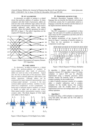
Figure 7: Test Bench Waveform for FFT using 4-
bit Vedic Multiplier](https://image.slidesharecdn.com/q041204105108-150115052013-conversion-gate02/85/High-Speed-Area-Efficient-8-point-FFT-using-Vedic-Multiplier-4-320.jpg)

This paper presents a high-speed 8-point Fast Fourier Transform (FFT) design utilizing a 4-bit Vedic multiplier and various adder configurations to enhance performance. It discusses the algorithms employed, including implementation details and simulation results that demonstrate improved execution time and lower power consumption. The findings suggest that the proposed multiplier can be effectively applied in digital signal processing and cryptography applications.