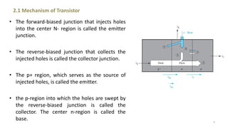
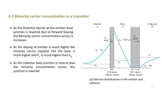
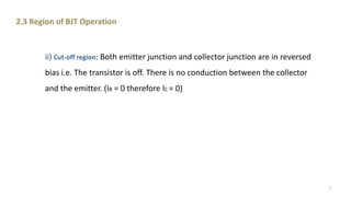
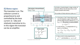
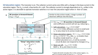
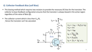
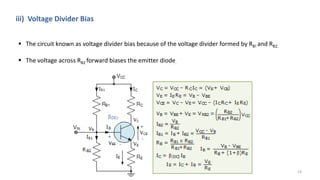
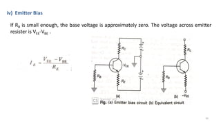
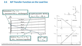
Lecture Notes
for
Semiconductor Devices and Circuits : BJT
Dr Pawan Kumar
Assistant Professor
Department of Physics
Mahatma Gandhi central university
Motihari-845401,Bihar
(Electronics : PHYS4008)
1
Contents
2
1.Transistor and type
2.BJT
2.1 Its Basic structure Mechanism of transistor
2.2 Minority carrier concentration in a transistor
2.3 Region of operation
2.4 Transistor connection
2.5 Transistor biasing
2.6 BJT Load line
1. Transistor & Type
Transistor
BJT (Bipolar) FET (Unipolar)
n-p-n p-n-p JFET MOSFET
 A transistor is a semiconductor device used to amplify or switch electronic signals and electrical power.
 It is composed of semiconductor material with at least three terminals for connection to an external
circuit.
3
2. Bipolar Junction transistor (BJT)
 It is a three terminals current controlled active device. It is called Bipolar as it lies on the two types of charge
carriers
 BJT consist of a Si (or Ge) crystal in which a layer of n type Si (or Ge) is sandwiched between two layer of p
type Si (or Ge) called p-n-p Transistor . Alternatively, a Transistor may also consist of a layer of p type Si (or
Ge) sandwiched between two layer of n type Si(or Ge) called n-p-n Transistor.
4
• The forward-biased junction that injects holes
into the center N- region is called the emitter
junction.
• The reverse-biased junction that collects the
injected holes is called the collector junction.
• The p+ region, which serves as the source of
injected holes, is called the emitter.
• the p-region into which the holes are swept by
the reverse-biased junction is called the
collector. The center n-region is called the
base.
2.1 Mechanism of Transistor
5
2.2 Minority carrier concentration in a transistor
(a) Electron distributions in the emitter and
collector
 As the Potential barrier at the emitter base
junction is lowered due to forward biasing
the Minority carrier concentration across it
increases.
 As the doping of emitter is much higher the
minority carrier injected into the base is
much higher and Pn is much higher than np.
 As the collector base junction is reverse bias
the minority concentration across this
junction is lowered
6
ii) Cut-off region: Both emitter junction and collector junction are in reversed
bias i.e. The transistor is off. There is no conduction between the collector
and the emitter. (IB = 0 therefore IC = 0)
2.3 Region of BJT Operation
7
ii) Active region:
The transistor is on. The
collector current is
proportional to and
controlled by the base
current (IC = βIB) and
relatively insensitive to VCE.
In this region the transistor
can be an amplifier.
8
•
iii) Saturation region: The transistor is on. The collector current varies very little with a change in the base current in the
saturation region. The VCE is small, a few tenths of a volt. The collector current is strongly dependent on VCE unlike in the
active region. It is desirable to operate transistor switches in or near the saturation region when in their on state.
9
2.4 Transistor connection
i) Common Base Connection
Input characteristics
10
11
Output characteristics
ii) Common Emitter Connection
Input characteristics
12
Output characteristics
iii) Common collector Connection
Input characteristics
14
Output characteristics
2.5 Transistor biasing circuit
i) Emitter feedback bias
 An increasing in the collector current
produces an increase in the voltage across the
emitter resistor, which reduces the base
current consequently the collector current.
 The emitter Resistor serves as the Feedback
element. If we adding voltage as a collector
then we get VCE+ IERE + IcRc – VCC =0
.
16
•
ii) Collector Feedback Bias (self Bias)
 This biasing method which requires two resistors to provide the necessary DC bias for the transistor. The
collector to base feedback configuration ensures that the transistor is always biased in the active region
regardless of the value of Beta (β).
 The collector current which is less than VCC/Rc
, Hence the transistor can’t be saturated.
18
•
iii) Voltage Divider Bias
 The circuit known as voltage divider bias because of the voltage divider formed by RB! and RB2.
 The voltage across RB2 forward biases the emitter diode.
19
iv) Emitter Bias
If RB is small enough, the base voltage is approximately zero. The voltage across emitter
resister is VEE-VBE .
20
21
2.6 BJT Transfer Function on the Load line
References
1. Solid state electronic devices by Ben G.streetman and S.K Banerjee
2. Lecture notes: Sec. 3 Sedra & Smith
3. Electronics devices and Circuit Theory By Robert L. Boylestad
4. Principle of electronic material and devices by S.O. Kasap.
5. Working Principle of MOSFET and MOSFET Characteristics
https://www.electrical4u.com/mosfet-working-principle-of-p-channel-n-channel-
mosfet/
22

Bipolar Junction Transistor theory and working

  • 1.
    Lecture Notes for Semiconductor Devicesand Circuits : BJT Dr Pawan Kumar Assistant Professor Department of Physics Mahatma Gandhi central university Motihari-845401,Bihar (Electronics : PHYS4008) 1
  • 2.
    Contents 2 1.Transistor and type 2.BJT 2.1Its Basic structure Mechanism of transistor 2.2 Minority carrier concentration in a transistor 2.3 Region of operation 2.4 Transistor connection 2.5 Transistor biasing 2.6 BJT Load line
  • 3.
    1. Transistor &Type Transistor BJT (Bipolar) FET (Unipolar) n-p-n p-n-p JFET MOSFET  A transistor is a semiconductor device used to amplify or switch electronic signals and electrical power.  It is composed of semiconductor material with at least three terminals for connection to an external circuit. 3
  • 4.
    2. Bipolar Junctiontransistor (BJT)  It is a three terminals current controlled active device. It is called Bipolar as it lies on the two types of charge carriers  BJT consist of a Si (or Ge) crystal in which a layer of n type Si (or Ge) is sandwiched between two layer of p type Si (or Ge) called p-n-p Transistor . Alternatively, a Transistor may also consist of a layer of p type Si (or Ge) sandwiched between two layer of n type Si(or Ge) called n-p-n Transistor. 4
  • 5.
    • The forward-biasedjunction that injects holes into the center N- region is called the emitter junction. • The reverse-biased junction that collects the injected holes is called the collector junction. • The p+ region, which serves as the source of injected holes, is called the emitter. • the p-region into which the holes are swept by the reverse-biased junction is called the collector. The center n-region is called the base. 2.1 Mechanism of Transistor 5
  • 6.
    2.2 Minority carrierconcentration in a transistor (a) Electron distributions in the emitter and collector  As the Potential barrier at the emitter base junction is lowered due to forward biasing the Minority carrier concentration across it increases.  As the doping of emitter is much higher the minority carrier injected into the base is much higher and Pn is much higher than np.  As the collector base junction is reverse bias the minority concentration across this junction is lowered 6
  • 7.
    ii) Cut-off region:Both emitter junction and collector junction are in reversed bias i.e. The transistor is off. There is no conduction between the collector and the emitter. (IB = 0 therefore IC = 0) 2.3 Region of BJT Operation 7
  • 8.
    ii) Active region: Thetransistor is on. The collector current is proportional to and controlled by the base current (IC = βIB) and relatively insensitive to VCE. In this region the transistor can be an amplifier. 8
  • 9.
    • iii) Saturation region:The transistor is on. The collector current varies very little with a change in the base current in the saturation region. The VCE is small, a few tenths of a volt. The collector current is strongly dependent on VCE unlike in the active region. It is desirable to operate transistor switches in or near the saturation region when in their on state. 9
  • 10.
    2.4 Transistor connection i)Common Base Connection Input characteristics 10
  • 11.
  • 12.
    ii) Common EmitterConnection Input characteristics 12
  • 13.
  • 14.
    iii) Common collectorConnection Input characteristics 14
  • 15.
  • 16.
    2.5 Transistor biasingcircuit i) Emitter feedback bias  An increasing in the collector current produces an increase in the voltage across the emitter resistor, which reduces the base current consequently the collector current.  The emitter Resistor serves as the Feedback element. If we adding voltage as a collector then we get VCE+ IERE + IcRc – VCC =0 . 16
  • 18.
    • ii) Collector FeedbackBias (self Bias)  This biasing method which requires two resistors to provide the necessary DC bias for the transistor. The collector to base feedback configuration ensures that the transistor is always biased in the active region regardless of the value of Beta (β).  The collector current which is less than VCC/Rc , Hence the transistor can’t be saturated. 18
  • 19.
    • iii) Voltage DividerBias  The circuit known as voltage divider bias because of the voltage divider formed by RB! and RB2.  The voltage across RB2 forward biases the emitter diode. 19
  • 20.
    iv) Emitter Bias IfRB is small enough, the base voltage is approximately zero. The voltage across emitter resister is VEE-VBE . 20
  • 21.
    21 2.6 BJT TransferFunction on the Load line
  • 22.
    References 1. Solid stateelectronic devices by Ben G.streetman and S.K Banerjee 2. Lecture notes: Sec. 3 Sedra & Smith 3. Electronics devices and Circuit Theory By Robert L. Boylestad 4. Principle of electronic material and devices by S.O. Kasap. 5. Working Principle of MOSFET and MOSFET Characteristics https://www.electrical4u.com/mosfet-working-principle-of-p-channel-n-channel- mosfet/ 22