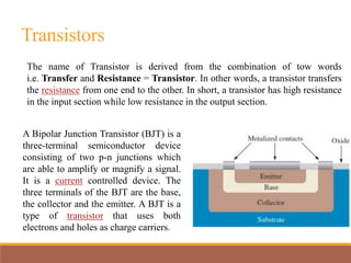
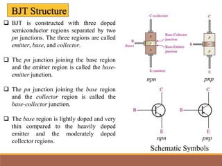
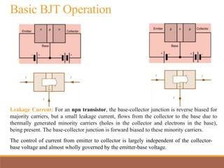
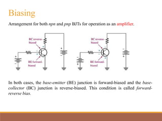
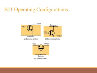
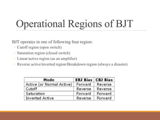
ANALOG ELECTRONICS
TRANSISTORS AND APPLICATIONS
LECTURE 13
Transistors
The name of Transistor is derived from the combination of tow words
i.e. Transfer and Resistance = Transistor. In other words, a transistor transfers
the resistance from one end to the other. In short, a transistor has high resistance
in the input section while low resistance in the output section.
A Bipolar Junction Transistor (BJT) is a
three-terminal semiconductor device
consisting of two p-n junctions which
are able to amplify or magnify a signal.
It is a current controlled device. The
three terminals of the BJT are the base,
the collector and the emitter. A BJT is a
type of transistor that uses both
electrons and holes as charge carriers.
BJT Structure
 BJT is constructed with three doped
semiconductor regions separated by two
pn junctions. The three regions are called
emitter, base, and collector.
 The pn junction joining the base region
and the emitter region is called the base-
emitter junction.
 The pn junction joining the base region
and the collector region is called the
base-collector junction.
 The base region is lightly doped and very
thin compared to the heavily doped
emitter and the moderately doped
collector regions.
npn pnp
npn pnp
Schematic Symbols
The control of current from emitter to collector is largely independent of the collector-
base voltage and almost wholly governed by the emitter-base voltage.
Basic BJT Operation
Leakage Current: For an npn transistor, the base-collector junction is reverse biased for
majority carriers, but a small leakage current, flows from the collector to the base due to
thermally generated minority carriers (holes in the collector and electrons in the base),
being present. The base-collector junction is forward biased to these minority carriers.
It is because a transistor makes use of both types of charge carriers (holes and
electrons) that they are called bipolar. The transistor also comprises two p-n
junctions and for this reason it is a junction transistor; hence the name –
bipolar junction transistor.
𝐼𝐸 = 𝐼𝐶 + 𝐼𝐵
Both majority and minority carriers contribute towards the total current flow
(Arrow shows conventional direction here)
Transistor Currents
Biasing
Arrangement for both npn and pnp BJTs for operation as an amplifier.
In both cases, the base-emitter (BE) junction is forward-biased and the base-
collector (BC) junction is reverse-biased. This condition is called forward-
reverse bias.
BJT Characteristics and Parameters
npn pnp
VBB forward-biases the base-emitter junction
VCC reverse-biases the base-collector junction
IB: dc base current
IE: dc emitter current
IC: dc collector current
VBE: dc voltage at base with respect to emitter
VCB: dc voltage at collector with respect to base
VCE: dc voltage at collector with respect to emitter
BJT Operating Configurations
Input & Output characteristics of BJT
Input characteristics Relation between IB and VBE
Output characteristics:
Relation between IC and VCE
Input Characteristics
Output Characteristics
Operational Regions of BJT
BJT operates in one of following four region:
◦ Cutoff region (open switch)
◦ Saturation region (closed switch)
◦ Linear/active region (as an amplifier)
◦ Reverse active/inverted region/Breakdown region (always a disaster)

Lec-13.pptx

  • 1.
    ANALOG ELECTRONICS TRANSISTORS ANDAPPLICATIONS LECTURE 13
  • 2.
    Transistors The name ofTransistor is derived from the combination of tow words i.e. Transfer and Resistance = Transistor. In other words, a transistor transfers the resistance from one end to the other. In short, a transistor has high resistance in the input section while low resistance in the output section. A Bipolar Junction Transistor (BJT) is a three-terminal semiconductor device consisting of two p-n junctions which are able to amplify or magnify a signal. It is a current controlled device. The three terminals of the BJT are the base, the collector and the emitter. A BJT is a type of transistor that uses both electrons and holes as charge carriers.
  • 3.
    BJT Structure  BJTis constructed with three doped semiconductor regions separated by two pn junctions. The three regions are called emitter, base, and collector.  The pn junction joining the base region and the emitter region is called the base- emitter junction.  The pn junction joining the base region and the collector region is called the base-collector junction.  The base region is lightly doped and very thin compared to the heavily doped emitter and the moderately doped collector regions. npn pnp npn pnp Schematic Symbols
  • 4.
    The control ofcurrent from emitter to collector is largely independent of the collector- base voltage and almost wholly governed by the emitter-base voltage. Basic BJT Operation Leakage Current: For an npn transistor, the base-collector junction is reverse biased for majority carriers, but a small leakage current, flows from the collector to the base due to thermally generated minority carriers (holes in the collector and electrons in the base), being present. The base-collector junction is forward biased to these minority carriers.
  • 5.
    It is becausea transistor makes use of both types of charge carriers (holes and electrons) that they are called bipolar. The transistor also comprises two p-n junctions and for this reason it is a junction transistor; hence the name – bipolar junction transistor. 𝐼𝐸 = 𝐼𝐶 + 𝐼𝐵 Both majority and minority carriers contribute towards the total current flow (Arrow shows conventional direction here) Transistor Currents
  • 6.
    Biasing Arrangement for bothnpn and pnp BJTs for operation as an amplifier. In both cases, the base-emitter (BE) junction is forward-biased and the base- collector (BC) junction is reverse-biased. This condition is called forward- reverse bias.
  • 7.
    BJT Characteristics andParameters npn pnp VBB forward-biases the base-emitter junction VCC reverse-biases the base-collector junction IB: dc base current IE: dc emitter current IC: dc collector current VBE: dc voltage at base with respect to emitter VCB: dc voltage at collector with respect to base VCE: dc voltage at collector with respect to emitter
  • 8.
  • 9.
    Input & Outputcharacteristics of BJT
  • 10.
    Input & Outputcharacteristics of BJT Input characteristics Relation between IB and VBE Output characteristics: Relation between IC and VCE
  • 11.
  • 12.
  • 13.
    Operational Regions ofBJT BJT operates in one of following four region: ◦ Cutoff region (open switch) ◦ Saturation region (closed switch) ◦ Linear/active region (as an amplifier) ◦ Reverse active/inverted region/Breakdown region (always a disaster)